EP1187412A2 - Carrier frequency recovery in CDMA receivers - Google Patents
Carrier frequency recovery in CDMA receivers Download PDFInfo
- Publication number
- EP1187412A2 EP1187412A2 EP01121170A EP01121170A EP1187412A2 EP 1187412 A2 EP1187412 A2 EP 1187412A2 EP 01121170 A EP01121170 A EP 01121170A EP 01121170 A EP01121170 A EP 01121170A EP 1187412 A2 EP1187412 A2 EP 1187412A2
- Authority
- EP
- European Patent Office
- Prior art keywords
- outputting
- output
- frequency
- signal
- despreader
- Prior art date
- Legal status (The legal status is an assumption and is not a legal conclusion. Google has not performed a legal analysis and makes no representation as to the accuracy of the status listed.)
- Withdrawn
Links
- 238000011084 recovery Methods 0.000 title 1
- 238000001514 detection method Methods 0.000 claims abstract description 33
- 230000010355 oscillation Effects 0.000 claims abstract description 32
- 239000000284 extract Substances 0.000 abstract description 3
- 238000004891 communication Methods 0.000 description 9
- 230000005540 biological transmission Effects 0.000 description 5
- NCGICGYLBXGBGN-UHFFFAOYSA-N 3-morpholin-4-yl-1-oxa-3-azonia-2-azanidacyclopent-3-en-5-imine;hydrochloride Chemical compound Cl.[N-]1OC(=N)C=[N+]1N1CCOCC1 NCGICGYLBXGBGN-UHFFFAOYSA-N 0.000 description 1
- 238000010586 diagram Methods 0.000 description 1
- 238000010295 mobile communication Methods 0.000 description 1
- 238000004904 shortening Methods 0.000 description 1
Images
Classifications
-
- H—ELECTRICITY
- H04—ELECTRIC COMMUNICATION TECHNIQUE
- H04L—TRANSMISSION OF DIGITAL INFORMATION, e.g. TELEGRAPHIC COMMUNICATION
- H04L27/00—Modulated-carrier systems
- H04L27/0014—Carrier regulation
-
- H—ELECTRICITY
- H04—ELECTRIC COMMUNICATION TECHNIQUE
- H04L—TRANSMISSION OF DIGITAL INFORMATION, e.g. TELEGRAPHIC COMMUNICATION
- H04L27/00—Modulated-carrier systems
- H04L27/0014—Carrier regulation
- H04L2027/0024—Carrier regulation at the receiver end
- H04L2027/0026—Correction of carrier offset
- H04L2027/0028—Correction of carrier offset at passband only
-
- H—ELECTRICITY
- H04—ELECTRIC COMMUNICATION TECHNIQUE
- H04L—TRANSMISSION OF DIGITAL INFORMATION, e.g. TELEGRAPHIC COMMUNICATION
- H04L27/00—Modulated-carrier systems
- H04L27/0014—Carrier regulation
- H04L2027/0044—Control loops for carrier regulation
- H04L2027/0053—Closed loops
- H04L2027/0055—Closed loops single phase
Definitions
- the present invention relates to a frequency adjusting circuit in a code division multiple access (to be referred to as a CDMA hereinafter) communication system, which performs adjustment to make the frequency of cosine and sine waves to be used for demodulation match the carrier frequency of a received CDMA modulated wave.
- a CDMA code division multiple access
- CDMA communication systems are currently being standardized by the 3GPP (Third Generation Partnership Project) as a standardization project that examines the international standard of third generation mobile communication systems.
- 3GPP Third Generation Partnership Project
- the specifications of a physical channel of a CDMA communication system and the like are defined by the 3GPP.
- Transmission signal (Di + jDq) ⁇ (Ci + jCq)
- the transmission signal is received by the receiving section of a base station or terminal and demodulated by multiplying it by the complex conjugate of the spreading code, as indicated by
- SCHs synchronization channels
- P-SCH first synchronization channel
- S-SCH second synchronization channel
- a CDMA communication system In a CDMA communication system, the receiving side must adjust the frequency of cosine and sine waves to be used for demodulation such that the value of the frequency of the cosine and sine waves to be used for demodulation matches the value of the frequency of the carrier wave.
- a CDMA communication system generally has a frequency adjusting circuit for adjusting the frequency to be used for demodulation.
- a conventional frequency adjusting circuit In a conventional frequency adjusting circuit, synchronization is established using a synchronization channel (to be referred to as an SCH hereinafter) and then the frequency to be used for demodulation is adjusted using a common pilot channel (to be referred to as a CPICH hereinafter).
- a common pilot channel to be referred to as a CPICH hereinafter.
- the value of the frequency of cosine and sine waves to be used for demodulation is switched to some appropriate frequency values to obtain reception results at corresponding times, and the value of the frequency of the most likely one of the reception results is determined as the value of the frequency of the cosine and sine waves to be used for demodulation.
- the initial frequency error generated between the frequency of a carrier wave and that to be used for demodulation is closely related to the time until the first common control physical channel (to be referred to as a P-CCPCH hereinafter). For this reason, the frequency adjusting circuit preferably adjusts the frequency error to be used for demodulation. However, since the conventional frequency adjusting circuit selects the optimum frequency to be used for demodulation by trial and error, frequency adjustment is time-consuming.
- the conventional frequency adjusting circuit detects the initial frequency error at the stage of CPICH.
- the initial frequency error has not been eliminated yet. For this reason, even a place at which a radio wave from a base station arrives may be determined as an incommunicable zone at the stage of SCH due to the initial frequency error.
- the conventional frequency adjusting circuit has the following two problems.
- a frequency adjusting circuit comprising an oscillator for outputting cosine and sine waves, quadrature demodulation means for extracting and outputting a baseband signal of an in-phase component from a carrier wave input from an antenna using the cosine wave output from the oscillator and extracting and outputting a baseband signal of a quadrature component from the carrier wave using the sine wave output from the oscillator, a first A/D converter for converting the baseband signal of the in-phase component output from the quadrature demodulation means into a digital signal and outputting the digital signal, a second A/D converter for converting the baseband signal of the quadrature component output from the quadrature demodulation means into a digital signal and outputting the digital signal, a first despreader for despreading and outputting the signal output from the first A/D converter, a second despreader for despreading and outputting the signal output from the second A/D converter, frequency error detection means
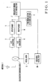
- Fig. 1 is a block diagram showing the arrangement of a frequency adjusting circuit of the present invention.
- Fig. 1 shows the arrangement of the frequency adjusting circuit of the present invention.
- the frequency adjusting circuit of the present invention comprises an antenna 1, quadrature demodulator 2, A/D converters 3 and 4, despreaders 5 and 6, frequency error detection section 7, synchronization detection section 8, oscillator 9, and reference oscillator 10.
- the antenna 1 receives a CDMA modulated carrier wave transmitted from a transmitting side.
- the quadrature demodulator 2 extracts and outputs the baseband signal of the in-phase component from the carrier wave input from the antenna using a cosine wave output from the oscillator 9, and also extracts and outputs the baseband signal of the quadrature component from the carrier wave using a sine wave output from the oscillator 9.
- the modulation scheme is BPSK (Bi-Phase Shift Keying)
- ⁇ 0, ⁇ .
- the second term of each of equations (7) and (8) is removed by an LPF (Low Pass Filter) (not shown) provided in the quadrature demodulator 2.
- LPF Low Pass Filter
- the quadrature demodulator 2 outputs 1/2cos( ⁇ wt + ⁇ ) as the baseband signal of the in-phase component and 1/2sin( ⁇ wt + ⁇ ) as the baseband signal of the quadrature component.
- the A/D converters 3 and 4 convert the baseband signal of the in-phase component and the baseband signal of the quadrature component, which are extracted by the quadrature demodulator 2, into digital signals, respectively.
- the baseband signal of the in-phase component and the baseband signal of the baseband signal, which are converted into digital signals, are input to the despreaders 5 and 6 and despread by the above-described spreading code.
- the synchronization detection section 8 acquires a synchronization signal from each despread signal and detects/holds its synchronization timing.
- synchronization is detected/held, e.g., the output from a data decoder (not shown) connected to each of the despreaders 5 and 6 is received as decoded data.
- the frequency error detection section 7 obtains the values given by equations (9) and (10) several times, detects the angular frequency error ⁇ w from those values, and outputs the angular frequency error ⁇ w.
- the number of times of obtaining the values given by equations (9) and (10) can be arbitrarily set in accordance with the channel reception state.
- the number of times may be automatically changed in correspondence with, e.g., the C/N (Carrier/Noise) ratio.
- the reference oscillator 10 changes the value of the oscillation frequency of the oscillator 9, i.e., the frequency of the cosine and sine waves to be output and outputs the frequency such that the value of the angular frequency error ⁇ w to be output from the frequency error detection section 7 becomes small.
- the initial frequency error is detected by the SCH when the modulation scheme of the channel to be calculated is the BPSK scheme.
- the modulation scheme of the channel to be calculated is the QPSK (Quad-Phase Shift Keying) scheme
- the frequency error detection section 7 can detect the frequency error by obtaining not the square but the fourth power of the value of each baseband signal.
- the frequency adjusting circuit of the present invention since the frequency adjusting circuit of the present invention has the frequency error detection section 7 capable of detecting the value of the initial frequency error between the frequency of the carrier wave and that of the cosine and sine waves to be used for demodulation, the initial frequency error can be quickly corrected. Hence, the frequency adjusting circuit of the present invention can shorten the time until P-CCPCH.
- the frequency adjusting circuit of the present invention detects the initial frequency error at the stage of SCH, the initial frequency error can be corrected at the stage of SCH.
- any incommunicable zone determination for a mobile station due to an initial frequency error in the range of a radio wave can be prevented.
Landscapes
- Engineering & Computer Science (AREA)
- Computer Networks & Wireless Communication (AREA)
- Signal Processing (AREA)
- Digital Transmission Methods That Use Modulated Carrier Waves (AREA)
- Synchronisation In Digital Transmission Systems (AREA)
Abstract
Description
- Di:
- transmission data of in-phase component
- Dq:
- transmission data of quadrature component
- Ci:
- in-phase component spreading code
- Cq:
- quadrature component spreading code
- j:
- imaginary number


Claims (16)
- A frequency adjusting circuit characterized by comprising:an oscillator (9) for outputting cosine and sine waves;quadrature demodulation means (2) for extracting and outputting a baseband signal of an in-phase component from a carrier wave input from an antenna using the cosine wave output from said oscillator and extracting and outputting a baseband signal of a quadrature component from the carrier wave using the sine wave output from said oscillator;a first A/D converter (3) for converting the baseband signal of the in-phase component output from said quadrature demodulation means (2) into a digital signal and outputting the digital signal;a second A/D converter (4) for converting the baseband signal of the quadrature component output from said quadrature demodulation means into a digital signal and outputting the digital signal;a first despreader (5) for despreading and outputting the signal output from said first A/D converter (3);a second despreader (6) for despreading and outputting the signal output from said second A/D converter (4);frequency error detection means (7) for detecting an error between a frequency of the carrier wave and a frequency of the cosine and sine waves output from said oscillator in accordance with a value of the signal output from said first despreader (5) and a value of the signal output from said second despreader (6); anda reference oscillator (10) for outputting a value of an oscillation frequency as the frequency of the cosine and sine waves to be output from said oscillator (9) and changing a value of the oscillation frequency so as to cancel the frequency error detected by said frequency error detection means (7).
- A circuit according to claim 1, wherein the frequency error is detected at a synchronization channel.
- A frequency adjusting circuit characterized by comprising:an oscillator (9) for outputting cosine and sine waves;quadrature demodulation means (2) for extracting and outputting a baseband signal of an in-phase component from a BPSK modulated wave of a synchronization channel input from an antenna using the cosine wave output from said oscillator and extracting and outputting a baseband signal of a quadrature component from the carrier wave using the sine wave output from said oscillator;a first A/D converter (3) for converting the baseband signal of the in-phase component output from said quadrature demodulation means into a digital signal and outputting the digital signal;a second A/D converter (4) for converting the baseband signal of the quadrature component output from said quadrature demodulation means into a digital signal and outputting the digital signal;a first despreader (5) for despreading and outputting the signal output from said first A/D converter;a second despreader (6) for despreading and outputting the signal output from said second A/D converter;frequency error detection means (7) for obtaining a square value of each of a value of the signal output from said first despreader and a value of the signal output from said second despreader several times and detecting, from the square values, an error between a carrier frequency of the modulated wave and a frequency of the cosine and sine waves output from said oscillator; anda reference oscillator (10) for outputting a value of an oscillation frequency as the frequency of the cosine and sine waves to be output from said oscillator and changing a value of the oscillation frequency so as to cancel the frequency error detected by said frequency error detection means (7).
- A circuit according to claim 3, wherein the frequency error is detected at the synchronization channel.
- A frequency adjusting circuit characterized by comprising:an oscillator (9) for outputting cosine and sine waves;quadrature demodulation means (2) for extracting and outputting a baseband signal of an in-phase component from a QPSK modulated wave of a synchronization channel input from an antenna using the cosine wave output from said oscillator and extracting and outputting a baseband signal of a quadrature component from the carrier wave using the sine wave output from said oscillator;a first A/D converter (3) for converting the baseband signal of the in-phase component output from said quadrature demodulation means into a digital signal and outputting the digital signal;a second A/D converter (4) for converting the baseband signal of the quadrature component output from said quadrature demodulation means into a digital signal and outputting the digital signal;a first despreader (5) for despreading and outputting the signal output from said first A/D converter;a second despreader (6) for despreading and outputting the signal output from said second A/D converter;frequency error detection means (7) for obtaining a fourth power of each of a value of the signal output from said first despreader and a value of the signal output from said second despreader several times and detecting, from the fourth powers, an error between a carrier frequency of the modulated wave and a frequency of the cosine and sine waves output from said oscillator; anda reference oscillator (10) for outputting a value of an oscillation frequency as the frequency of the cosine and sine waves to be output from said oscillator (9) and changing a value of the oscillation frequency so as to cancel the frequency error detected by said frequency error detection means.
- A circuit according to claim 5, wherein the frequency error is detected at the synchronization channel.
- A frequency adjusting circuit characterized by comprising:oscillation means (9) for outputting an oscillation frequency of cosine and sine waves;quadrature demodulation means (2) for extracting and outputting a baseband signal of an in-phase component from a carrier wave of a received modulated wave using the cosine wave and extracting and outputting a baseband signal of a quadrature component from the received modulated carrier wave using the sine wave;a first A/D converter (3) for converting the baseband signal of the in-phase component output from said quadrature demodulation means into a digital signal and outputting the digital signal;a second A/D converter (4) for converting the baseband signal of the quadrature component output from said quadrature demodulation means into a digital signal and outputting the digital signal;a first despreader (5) for despreading and outputting the signal output from said first A/D converter;a second despreader (6) for despreading and outputting the signal output from said second A/D converter;frequency error detection means (7) for detecting an error between a frequency of the carrier wave and the oscillation frequency of the cosine and sine waves in accordance with a value of the signal output from said first despreader and a value of the signal output from said second despreader; andmeans (10) for changing the oscillation frequency so as to cancel the frequency error detected by said frequency error detection means.
- A circuit according to claim 7, wherein the frequency error is detected at a synchronization channel.
- A code division multiple access receiver characterized by comprising:an antenna (1) for receiving a code division multiple access modulated wave;an oscillator (9) for outputting cosine and sine waves;quadrature demodulation means (2) for extracting and outputting a baseband signal of an in-phase component from a carrier wave of the received modulated wave using the cosine wave output from said oscillator and extracting and outputting a baseband signal of a quadrature component from the carrier wave using the sine wave output from said oscillator;a first A/D converter (3) for converting the baseband signal of the in-phase component output from said quadrature demodulation means into a digital signal and outputting the digital signal;a second A/D converter (4) for converting the baseband signal of the quadrature component output from said quadrature demodulation means into a digital signal and outputting the digital signal;a first despreader (5) for despreading and outputting the signal output from said first A/D converter;a second despreader (6) for despreading and outputting the signal output from said second A/D converter;frequency error detection means (7) for detecting an error between a frequency of the carrier wave and a frequency of the cosine and sine waves output from said oscillator in accordance with a value of the signal output from said first despreader and a value of the signal output from said second despreader; anda reference oscillator (10) for outputting a value of an oscillation frequency as the frequency of the cosine and sine waves to be output from said oscillator and changing a value of the oscillation frequency so as to cancel the frequency error detected by said frequency error detection means.
- A receiver according to claim 9, wherein the frequency error is detected at a synchronization channel.
- A code division multiple access receiver
characterized by comprising:an antenna (1) for receiving a code division multiple access modulated wave;an oscillator (9) for outputting cosine and sine waves;quadrature demodulation means (2) for extracting and outputting a baseband signal of an in-phase component from a BPSK modulated wave of a synchronization channel of the received code division multiple access modulated wave using the cosine wave output from said oscillator and extracting and outputting a baseband signal of a quadrature component from the carrier wave using the sine wave output from said oscillator;a first A/D converter (3) for converting the baseband signal of the in-phase component output from said quadrature demodulation means into a digital signal and outputting the digital signal;a second A/D converter (4) for converting the baseband signal of the quadrature component output from said quadrature demodulation means into a digital signal and outputting the digital signal;a first despreader (5) for despreading and outputting the signal output from said first A/D converter;a second despreader (6) for despreading and outputting the signal output from said second A/D converter;frequency error detection means (7) for obtaining a square value of each of a value of the signal output from said first despreader and a value of the signal output from said second despreader several times and detecting, from the square values, an error between a carrier frequency of the BPSK modulated wave and a frequency of the cosine and sine waves output from said oscillator; anda reference oscillator (10) for outputting a value of an oscillation frequency as the frequency of the cosine and sine waves to be output from said oscillator and changing a value of the oscillation frequency so as to cancel the frequency error detected by said frequency error detection means. - A code division multiple access receiver characterized by comprising:an antenna (1) for receiving a code division multiple access modulated wave;an oscillator (9) for outputting cosine and sine waves;quadrature demodulation means (2) for extracting and outputting a baseband signal of an in-phase component from a QPSK modulated wave of a synchronization channel of the modulated wave using the cosine wave output from said oscillator and extracting and outputting a baseband signal of a quadrature component from the carrier wave using the sine wave output from said oscillator;a first A/D converter (3) for converting the baseband signal of the in-phase component output from said quadrature demodulation means into a digital signal and outputting the digital signal;a second A/D converter (4) for converting the baseband signal of the quadrature component output from said quadrature demodulation means into a digital signal and outputting the digital signal;a first despreader (5) for despreading and outputting the signal output from said first A/D converter;a second despreader (6) for despreading and outputting the signal output from said second A/D converter;frequency error detection means (7) for obtaining a fourth power of each of a value of the signal output from said first despreader and a value of the signal output from said second despreader several times and detecting, from the fourth powers, an error between a carrier frequency of the QPSK modulated wave and a frequency of the cosine and sine waves output from said oscillator; anda reference oscillator (10) for outputting a value of an oscillation frequency as the frequency of the cosine and sine waves to be output from said oscillator and changing a value of the oscillation frequency so as to cancel the frequency error detected by said frequency error detection means.
- A code division multiple access receiver characterized by comprising:an antenna (1) for receiving a code division multiple access modulated wave;oscillation means (9) for outputting an oscillation frequency of cosine and sine waves;quadrature demodulation means (2) for extracting and outputting a baseband signal of an in-phase component from a carrier wave of the received modulated wave using the cosine wave and extracting and outputting a baseband signal of a quadrature component from the carrier wave using the sine wave;a first A/D converter (3) for converting the baseband signal of the in-phase component output from said quadrature demodulation means into a digital signal and outputting the digital signal;a second A/D converter (4) for converting the baseband signal of the quadrature component output from said quadrature demodulation means into a digital signal and outputting the digital signal;a first despreader (5) for despreading and outputting the signal output from said first A/D converter;a second despreader (6) for despreading and outputting the signal output from said second A/D converter;frequency error detection means (7) for detecting an error between a frequency of the carrier wave and the oscillation frequency of the cosine and sine waves in accordance with a value of the signal output from said first despreader and a value of the signal output from said second despreader; andmeans (10) for changing the oscillation frequency so as to cancel the frequency error detected by said frequency error detection means.
- A receiver according to claim 13, wherein the frequency error is detected at a synchronization channel.
- A code division multiple access receiver characterized by comprising:an antenna (1) for receiving a code division multiple access modulated wave;oscillation means (9) for outputting an oscillation frequency of cosine and sine waves;quadrature demodulation means (2) for extracting and outputting a baseband signal of an in-phase component from a BPSK modulated wave of a synchronization channel of the received code division multiple access modulated wave using the cosine wave and extracting and outputting a baseband signal of a quadrature component from the carrier wave using the sine wave;a first A/D converter (3) for converting the baseband signal of the in-phase component output from said quadrature demodulation means into a digital signal and outputting the digital signal;a second A/D converter (4) for converting the baseband signal of the quadrature component output from said quadrature demodulation means into a digital signal and outputting the digital signal;a first despreader (5) for despreading and outputting the signal output from said first A/D converter;a second despreader (6) for despreading and outputting the signal output from said second A/D converter;frequency error detection means (7) for obtaining a square value of each of a value of the signal output from said first despreader and a value of the signal output from said second despreader several times and detecting, from the square values, an error between a carrier frequency of the BPSK modulated wave and the oscillation frequency of the cosine and sine waves; andmeans (10) for changing the oscillation frequency so as to cancel the frequency error detected by said frequency error detection means.
- A code division multiple access receiver characterized by comprising:an antenna (1) for receiving a code division multiple access modulated wave;an oscillator (9) for outputting an oscillation frequency of cosine and sine waves;quadrature demodulation means (2) for extracting and outputting a baseband signal of an in-phase component from a QPSK modulated wave of a synchronization channel of the modulated wave using the cosine wave and extracting and outputting a baseband signal of a quadrature component from the carrier wave using the sine wave;a first A/D converter (3) for converting the baseband signal of the in-phase component output from said quadrature demodulation means into a digital signal and outputting the digital signal;a second A/D converter (4) for converting the baseband signal of the quadrature component output from said quadrature demodulation means into a digital signal and outputting the digital signal;a first despreader (5) for despreading and outputting the signal output from said first A/D converter;a second despreader (6) for despreading and outputting the signal output from said second A/D converter;frequency error detection means (7) for obtaining a fourth power of each of a value of the signal output from said first despreader and a value of the signal output from said second despreader several times and detecting, from the fourth powers, an error between a carrier frequency of the QPSK modulated wave and the oscillation frequency of the cosine and sine waves output; andmeans (10) for changing the oscillation frequency so as to cancel the frequency error detected by said frequency error detection means.
Applications Claiming Priority (2)
| Application Number | Priority Date | Filing Date | Title |
|---|---|---|---|
| JP2000268783 | 2000-09-05 | ||
| JP2000268783A JP2002076992A (en) | 2000-09-05 | 2000-09-05 | Frequency adjusting circuit |
Publications (2)
| Publication Number | Publication Date |
|---|---|
| EP1187412A2 true EP1187412A2 (en) | 2002-03-13 |
| EP1187412A3 EP1187412A3 (en) | 2005-07-27 |
Family
ID=18755509
Family Applications (1)
| Application Number | Title | Priority Date | Filing Date |
|---|---|---|---|
| EP01121170A Withdrawn EP1187412A3 (en) | 2000-09-05 | 2001-09-04 | Carrier frequency recovery in CDMA receivers |
Country Status (5)
| Country | Link |
|---|---|
| US (1) | US6556619B2 (en) |
| EP (1) | EP1187412A3 (en) |
| JP (1) | JP2002076992A (en) |
| CN (1) | CN1153390C (en) |
| AU (1) | AU774123B2 (en) |
Cited By (3)
| Publication number | Priority date | Publication date | Assignee | Title |
|---|---|---|---|---|
| WO2003103248A1 (en) * | 2002-05-31 | 2003-12-11 | Advanced Micro Devices, Inc. | Phase error correction using despread signals |
| US7190713B2 (en) | 2002-05-31 | 2007-03-13 | Advanced Micro Devices, Inc. | Phase error correction using despread signals |
| US7454743B2 (en) | 2001-12-28 | 2008-11-18 | Sun Microsystems, Inc. | Java to SNMP MIB mapping |
Families Citing this family (4)
| Publication number | Priority date | Publication date | Assignee | Title |
|---|---|---|---|---|
| WO2003034588A1 (en) * | 2001-10-12 | 2003-04-24 | Mitsubishi Denki Kabushiki Kaisha | Amplifier apparatus and receiver |
| US7038552B2 (en) * | 2003-10-07 | 2006-05-02 | Analog Devices, Inc. | Voltage controlled oscillator having improved phase noise |
| EP1542418A1 (en) * | 2003-12-10 | 2005-06-15 | Telefonaktiebolaget LM Ericsson (publ) | Wireless multicarrier system with subcarriers reserved for communication between unsynchronized nodes |
| US7369606B1 (en) | 2004-02-19 | 2008-05-06 | L-3 Communications Corporation | Phase error detector using I/Q interference cancellation |
Family Cites Families (11)
| Publication number | Priority date | Publication date | Assignee | Title |
|---|---|---|---|---|
| DE69328814T2 (en) * | 1992-11-25 | 2001-01-18 | Nec Corp., Tokio/Tokyo | Frequency error measurement device for accurately detecting a frequency error between a carrier frequency and a standard frequency |
| JP2659060B2 (en) * | 1994-07-06 | 1997-09-30 | 日本電気株式会社 | Frequency error detection method |
| JP2728034B2 (en) * | 1995-06-15 | 1998-03-18 | 日本電気株式会社 | Spread spectrum signal receiver |
| US5799034A (en) * | 1995-12-06 | 1998-08-25 | Rockwell International Corporation | Frequency acquisition method for direct sequence spread spectrum systems |
| US5982821A (en) * | 1996-01-16 | 1999-11-09 | L-3 Communications | Frequency discriminator and method and receiver incorporating same |
| JP3310160B2 (en) * | 1996-03-29 | 2002-07-29 | 松下電器産業株式会社 | Spread spectrum receiver |
| JP3226807B2 (en) * | 1996-11-20 | 2001-11-05 | 静岡日本電気株式会社 | Automatic frequency correction apparatus and automatic frequency correction method for paging system |
| US6160838A (en) * | 1996-12-13 | 2000-12-12 | Uniden Corporation | Spread spectrum transmitter, spread spectrum receiver and spread spectrum communication method and automatic gain control circuit for spread spectrum receiver |
| JP2000209128A (en) * | 1999-01-18 | 2000-07-28 | Matsushita Electric Ind Co Ltd | Receiver |
| JP2000278344A (en) * | 1999-03-25 | 2000-10-06 | Sanyo Electric Co Ltd | Pseodo lock detection system |
| US6363102B1 (en) * | 1999-04-23 | 2002-03-26 | Qualcomm Incorporated | Method and apparatus for frequency offset correction |
-
2000
- 2000-09-05 JP JP2000268783A patent/JP2002076992A/en active Pending
-
2001
- 2001-09-04 EP EP01121170A patent/EP1187412A3/en not_active Withdrawn
- 2001-09-04 US US09/944,416 patent/US6556619B2/en not_active Expired - Fee Related
- 2001-09-05 CN CNB011410248A patent/CN1153390C/en not_active Expired - Fee Related
- 2001-09-05 AU AU67113/01A patent/AU774123B2/en not_active Ceased
Cited By (3)
| Publication number | Priority date | Publication date | Assignee | Title |
|---|---|---|---|---|
| US7454743B2 (en) | 2001-12-28 | 2008-11-18 | Sun Microsystems, Inc. | Java to SNMP MIB mapping |
| WO2003103248A1 (en) * | 2002-05-31 | 2003-12-11 | Advanced Micro Devices, Inc. | Phase error correction using despread signals |
| US7190713B2 (en) | 2002-05-31 | 2007-03-13 | Advanced Micro Devices, Inc. | Phase error correction using despread signals |
Also Published As
| Publication number | Publication date |
|---|---|
| CN1153390C (en) | 2004-06-09 |
| US20020027471A1 (en) | 2002-03-07 |
| CN1343049A (en) | 2002-04-03 |
| AU774123B2 (en) | 2004-06-17 |
| AU6711301A (en) | 2002-03-07 |
| JP2002076992A (en) | 2002-03-15 |
| EP1187412A3 (en) | 2005-07-27 |
| US6556619B2 (en) | 2003-04-29 |
Similar Documents
| Publication | Publication Date | Title |
|---|---|---|
| US5881098A (en) | Efficient demodulation scheme for DSSS communication | |
| EP0577044B1 (en) | Phase difference correcting demodulator for a receiver for spread spectrum communication and method of demodulating | |
| US5694417A (en) | Short burst direct acquisition direct sequence spread spectrum receiver | |
| EP0675606B1 (en) | Receiver for spread spectrum communication | |
| US5610939A (en) | Signal processing circuit for spread spectrum communications | |
| US5712870A (en) | Packet header generation and detection circuitry | |
| EP0682427B1 (en) | Correlation detector and communication apparatus | |
| US6507603B1 (en) | CDMA receiver | |
| US7027444B2 (en) | Apparatus and method for generating a preamble sequence in a wireless communication system | |
| EP0848504A2 (en) | Quadrature phase shift keying spread spectrum communication system | |
| US6853631B1 (en) | Code-division multiplex communication transmitting apparatus and receiving apparatus and method thereof | |
| US6327257B1 (en) | Code division multiple access transmitter and receiver | |
| EP1187412A2 (en) | Carrier frequency recovery in CDMA receivers | |
| US6950456B2 (en) | High-speed cell searching apparatus and method using DPSK-based distributed sample acquisition | |
| JP3418981B2 (en) | Spread spectrum communication synchronization acquisition circuit | |
| US6580748B1 (en) | Spread spectrum communication method and spread spectrum communication apparatus | |
| US7194046B2 (en) | Frequency error correction unit and method in a wireless LAN system | |
| US10491264B1 (en) | Combined demodulator and despreader | |
| US6831942B2 (en) | MPSK spread spectrum communications receiver with carrier recovery and tracking using weighted correlation techniques | |
| KR100245330B1 (en) | Phase and frequency detector of digital communication system | |
| JP2003008474A (en) | Spread spectrum communication unit | |
| KR950010928B1 (en) | Differential two-phase shift keying demodulator and demodulation method | |
| De Gaudenzi et al. | A frequency error resistant blind interference-mitigating CDMA detector | |
| KR100347529B1 (en) | Synchronous wideband CDMA demodulator structure for wireless packet communication | |
| EP1488586A1 (en) | Frequency error correction system with initial frequency estimation and feedback tracking |
Legal Events
| Date | Code | Title | Description |
|---|---|---|---|
| PUAI | Public reference made under article 153(3) epc to a published international application that has entered the european phase |
Free format text: ORIGINAL CODE: 0009012 |
|
| AK | Designated contracting states |
Kind code of ref document: A2 Designated state(s): AT BE CH CY DE DK ES FI FR GB GR IE IT LI LU MC NL PT SE TR |
|
| AX | Request for extension of the european patent |
Free format text: AL;LT;LV;MK;RO;SI |
|
| PUAL | Search report despatched |
Free format text: ORIGINAL CODE: 0009013 |
|
| AK | Designated contracting states |
Kind code of ref document: A3 Designated state(s): AT BE CH CY DE DK ES FI FR GB GR IE IT LI LU MC NL PT SE TR |
|
| AX | Request for extension of the european patent |
Extension state: AL LT LV MK RO SI |
|
| RIC1 | Information provided on ipc code assigned before grant |
Ipc: 7H 03D 1/22 B Ipc: 7H 04L 27/00 A |
|
| 17P | Request for examination filed |
Effective date: 20050617 |
|
| AKX | Designation fees paid |
Designated state(s): DE FR GB IT |
|
| STAA | Information on the status of an ep patent application or granted ep patent |
Free format text: STATUS: THE APPLICATION HAS BEEN WITHDRAWN |
|
| 18W | Application withdrawn |
Effective date: 20091016 |