EP1187328A2 - Low operational power, low leakage power D-type flip-flop - Google Patents
Low operational power, low leakage power D-type flip-flop Download PDFInfo
- Publication number
- EP1187328A2 EP1187328A2 EP01116203A EP01116203A EP1187328A2 EP 1187328 A2 EP1187328 A2 EP 1187328A2 EP 01116203 A EP01116203 A EP 01116203A EP 01116203 A EP01116203 A EP 01116203A EP 1187328 A2 EP1187328 A2 EP 1187328A2
- Authority
- EP
- European Patent Office
- Prior art keywords
- output
- flip
- flop
- power consumption
- state
- Prior art date
- Legal status (The legal status is an assumption and is not a legal conclusion. Google has not performed a legal analysis and makes no representation as to the accuracy of the status listed.)
- Withdrawn
Links
Images


Classifications
-
- H—ELECTRICITY
- H03—ELECTRONIC CIRCUITRY
- H03K—PULSE TECHNIQUE
- H03K19/00—Logic circuits, i.e. having at least two inputs acting on one output; Inverting circuits
- H03K19/0008—Arrangements for reducing power consumption
- H03K19/0016—Arrangements for reducing power consumption by using a control or a clock signal, e.g. in order to apply power supply
Definitions
- the invention relates to digital electronic circuits and, in particular, to a flip-flop that has low operational power consumption and low leakage power consumption and that additionally has a sleep mode. In the sleep mode, the output of the flip-flop is held in a state that sets a digital electronic circuit that includes the flip-flop to a low leakage power consumption state.
- Flip-Flops are the basic storage elements used in synchronous digital VLSI circuits and in other digital electronic circuits.
- Existing flip-flop designs include the following:
- Flip-flop designs 1 through 5, 7 and 13 are described by V. Stojanovic and V. Oklobdzija in Comparative Analysis of Master-Slave Latches and Flip-Flops for High-Performance and Low-Power Systems, 34 IEEE J. SOLID-STATE CIRCUITS, 536-548 (1999 April).
- Flip-flop designs 6, 8 and 9 are described by J. Wang, P. Yang and D. Sheng in Design of a 3V 300MHz Low-Power 8-b ⁇ 8-b Pipelined Multiplier Using Pulse-Triggered TSPC Flip-Flops, 35 IEEE J. SOLID STATE CIRCUITS (2000 April).
- Flip-flop design 10 is disclosed in United States patent no.
- Flip-flops are an integral component of digital circuits used for data storage. Hence, there is an important need for a flip-flop that not only has low operating power consumption but also has low leakage power consumption when the flip-flop is in a stand-by or sleep mode.
- a flip-flop design that not only has low operational power consumption and low leakage power consumption, but that is additionally capable of setting its output to a predefined state that is independent of the data state at either or both of the clock input and the data input to reduce the leakage power consumption of circuitry connected to the output of the flip-flop.
- a flip-flop whose power consumption is low when its output is held in the predefined state.
- some types of circuitry may have low leakage power consumption when the output of the flip-flop is in one state, while other types of circuitry may have low leakage power consumption when the output of the flip-flop is in the other state.
- a flip-flop capable of being fabricated in embodiments having low leakage power consumption when the predetermined state corresponds to either output state.
- the invention provides a flip-flop having a sleep mode in which power consumption is reduced.
- the flip-flop comprises a clock input, a data input, an input stage, an input gate, an output stage and an output clamp.
- the input gate is interposed between the data input and the input stage and operates in the sleep mode to isolate the input stage from the data input.
- the output stage is coupled to the input stage and includes an output having a first output state and a second output state.
- the output clamp operates in the sleep mode to set the output stage to a predetermined state regardless of the data states at the data input and the clock input.
- the predetermined state is the one of the output states in which the leakage power consumption of the flip-flop is less than in the other of the output states.
- the predetermined state may alternatively be the one of the output states in which the leakage power consumption of circuitry connected to the output of the flip-flop is less than in the other of the output states.
- the predetermined state may be the one of the output states in which the leakage power consumption of a digital electronic circuit of which the flip-flop forms part is less than in the other of the output states.
- the invention additionally provides a digital electronic circuit having a sleep mode in which power consumption is reduced.
- the electronic circuit comprises a data input and a flip-flop.
- the flip-flop includes a dock input, an input stage, an input gate, an output stage and an output clamp.
- the input gate is interposed between the data input and the input stage, and operates in the sleep mode to isolate the input stage from the data input.
- the output stage is coupled to the input stage and comprises an output having a first output state and a second output state.
- the output clamp operates in the sleep mode to set the output to a predetermined state regardless of the data states at the data input and the clock input.
- the predetermined state is the one of the output states in which the leakage power consumption of the digital electronic circuit is less than in the other of the output states.
- the invention provides a method of establishing, in a digital electronic circuit, a sleep mode in which power consumption of the digital electronic circuit is reduced.
- the power consumption includes leakage power consumption.
- the digital electronic circuit includes a data input and a flip-flop coupled to the data input.
- the flip flop has a clock input and a data output.
- the data input is isolated from the flip flop and the data output is set to a predetermined state regardless of data states at the data input and the clock input.
- the predetermined state is a state of the data output in which the leakage power consumption is reduced.
- Isolating the data input from the remainder of the flip-flop has the effect of not allowing any transitions to occur in the flip-flop while the flip-flop is in its sleep mode. This avoids the power consumption that such transitions would normally incur.
- Setting the output to the predetermined state sets the output to the output state that reduces the leakage power consumption of the digital electronic circuit composed of the flip-flop and the circuitry connected to the output of the flip-flop. Reducing the leakage power consumption of the digital electronic circuit involves reducing the leakage power consumption of either or both of the flip-flop and circuitry connected to the output of the flip-flop.
- the flip-flop, the digital electronic circuit and the method according to the invention provide a reduction in leakage power consumption not possible with the flip-flop designs described above.
- Figures 1 and 2 show two embodiments of a low-power flip-flop according to the invention. Both embodiments of the flip-flop have a sleep mode set by the control signal SLEEP in which the power consumption of the flip-flop is reduced. Figures 1 and 2 also show are two embodiments of a digital electronic circuit according to the invention of which the flip-flop according to the invention forms part. Both embodiments of the digital electronic circuit have a sleep mode set by the control signal SLEEP in which the power consumption of the circuit is reduced.
- Figure 1 shows the flip-flop 100 according to the invention forming part of the digital electronic circuit 10 according to the invention.
- the digital electronic circuit is additionally composed of the circuitry 12 connected to the output Q of the flip-flop.
- the circuitry 12 is composed of one or more circuits, such as combinatorial logic circuits, adders, multipliers, etc., that are typically controlled by, or operate in response to, the state of the output Q of the flip-flop.
- the leakage power consumption of the circuitry 12 depends on the state of the output Q. In this example, the leakage power consumption of the circuitry 12 is less wheh the output Q is in its high state (designated as 1) than when the output Q is in its low state (designated as 0 ).
- the flip-flop 100 is configured so that, in the sleep mode, the output Q is set to the 1 state regardless of the states of the data and clock inputs D and CLO, respectively, to reduce the leakage power consumption of the digital electronic circuit 10.
- FIG. 2 shows the flip-flop 200 according to the invention forming part of the digital electronic circuit 20 according to the invention.
- the digital electronic circuit is additionally composed of the circuitry 22 connected to the Q output of the flip-flop.
- the circuitry 22 is composed of one or more circuits that are typically controlled by, or operate in response to, the state of the output Q of the flip-flop.
- the leakage power consumption of the circuitry 22 depends on the state of the output Q. In this example, the leakage power consumption of the circuitry 22 is less when the output Q is in its 0 state than when the output Q is in its 1 state.
- the flip-flop 200 is configured so that, in its sleep mode, the output Q is set to its 0 state, regardless of the states of the data and clock inputs D and CLO, respectively, to reduce the leakage power consumption of the digital electronic circuit 20.
- the embodiments 100 and 200 shown in Figures 1 and 2, respectively, of the flip-flop according to the invention are based on the flip-flop design no. 8 referred to above, i.e., the Eight Transistor D-type flip-flop.
- This flip-flop design was chosen as the basis for the flip-flop according to the invention because, when implemented using the 0.25 micron process of Agilent Technologies, Inc., the assignee of the invention disclosed herein, it has the lowest power of all of the flip-flop designs 1-16 when these designs are implemented using the same process.
- the Eight Transistor D-type flip-flop design additionally has the advantage of implementing a true single-phase-clocking strategy. This strategy provides a compact and simple clock distribution without any extra timing considerations such as clock skew caused by the need to distribute both the clock and its inverse to each flip-flop.
- flip-flop design no. 8 basing the flip-flop according to the invention on flip-flop design no. 8 is not critical to the invention. It will be apparent to the person of ordinary skill in the art that flip-flop designs 1-7 and 9-16, and other flip-flop designs not mentioned above, can form the basis of the flip-flop according to the invention.
- the embodiment 100 of the flip-flop according to the invention will now be described with reference to Figure 1. Elements of the basic eight-transistor D-type flip-flop on which the flip-flop 100 is based will be described first.
- the eight-transistor D-type flip-flop is composed of input stage 102, transfer stage 104, output stage 106 and inverting output driver 108.
- circuitry 12 is connected to the output Q of the inverting output driver.
- the input stage 102 is composed of PMOS transistors 110 and 112 and NMOS transistor 114 arranged in order and in series between the positive supply V DD and ground.
- the gates of transistors 110 and 114 are connected to the data input D.
- the gate of transistor 112 is connected to the clock input CLO.
- the transfer stage 104 is composed of PMOS transistor 120 and NMOS transistors 122 and 124 arranged in order and in series between the positive supply V DD and ground.
- the gate of transistor 120 is connected to the node formed by the drain of transistor 110 and the source of transistor 112.
- the gate of transistor 122 is connected to the clock input CLO.
- the gate of transistor 124 is connected to the node formed by the drains of transistors 112 and 114.
- the output stage 106 is composed of PMOS transistor 130 and NMOS transistor 134 arranged in order and in series between the positive supply V DD and ground.
- the gate of transistor 130 is connected to the node formed by the drains of transistors 120 and 122.
- the gate of transistor 134 is connected to the node formed by the source of transistor 122 and the drain of transistor 124.
- the node between the drains of the transistors 130 and 134 provides the output Q-bar, and is conventionally connected to the input of the inverting output driver 108.
- the output of the inverting output driver provides the output Q of the flip-flop 100.
- the flip-flop 100 additionally includes the input gate 140 and the output clamp 150 and optionally includes the control signal generator 160.
- the input gate 140 is interposed between the data input D and the gates of transistors 110 and 114.
- the input gate is composed of NMOS transistor 142 and PMOS transistor 144 connected in parallel.
- the parallel combination is interposed between the data input and the gates of transistors 110 and 114.
- the gates of transistors 142 and 144 are connected to receive control signals SLOFF and SLON, respectively, generated by the control signal generator 160.
- the output clamp 150 is composed of PMOS transistor 152 interposed between transistors 130 and 134 in the output stage 106 and NMOS transistor 154 connected in parallel with transistor 134.
- the gates of transistors 152 and 154 are connected to receive control signal SLON from the control signal generator 160.
- the node to which the drains of the transistors 154, 152 and 134 are connected provides the Q-bar output and the input of the inverting output driver 108 is connected to this node.
- the control signal generator 160 is composed of inverters 162 and 164 connected in series.
- the input of inverter 162 receives the control signal SLEEP.
- the output of inverter 162 provides the control signal SLON and is connected to the input of the inverter 164 and the gates of transistors 144, 152 and 154.
- the output of inverter 164 provides the control signal SLOFF and is connected to the gate of transistor 142.
- the control signal generator is optional in the sense that more than one of the flip-flops 100 may be connected to receive the control signals SLON and SLOFF generated by a single control signal generator 160.
- the control signal SLEEP is generated by a circuit (not shown) that determines when to place the flip-flop 100 in its sleep mode. Placing the flip-flop in its sleep mode places the electronic circuit 10 in its sleep mode.
- the flip-flop 100 can be placed in its sleep mode not only when the entire electronic device of which the digital electronic circuit 10 forms part is idle, but also when the digital electronic circuit 10 is idle, even though other parts of the electronic device may continue to operate.
- digital electronic circuit 10 may form all or part of the data compression circuitry of a battery-operated electronic camera. The entire electronic camera typically enters a sleep mode if several minutes elapse without the user operating the camera. Moreover, even when the entire electronic camera is not in its sleep mode, the data compression circuitry can be placed in its sleep mode until a picture is taken and the data compression circuitry is required to operate to compress the resulting picture data.
- Design tools for ASICs and other types of integrated circuits can include capabilities that enable circuits for generating one or more SLEEP control signals to be included in the overall circuit design.
- circuits used to generate a control signal for clock gating circuits, described above can be used to generate a suitable SLEEP control signal.
- Such circuits may alternatively be configured to generate suitably buffered control signals equivalent to the control signals SLON and SLOFF generated by the control signal generator 160. In this case, the control signal generator can be omitted.
- control signal SLEEP is in its 1 state.
- This control signal is preferably an active low signal. Consequently, the control signals SLON and SLOFF are in their 0 and 1 states, respectively, which set the input gate 140 to its ON state and the output clamp 150 to its OFF state.
- control signal SLOFF in its 1 state sets the transistor 142 to its ON state and the control signal SLON in its 0 state sets the transistor 144 to its ON state to set the input gate to its ON state
- control signal SLON in its 0 state sets the transistor 152 to its ON state and sets the transistor 154 to its OFF state to set the output clamp to its OFF state.
- the flip-flop 100 operates as a conventional single rising edge-triggered D-flip-flop, as will be described next.
- the input data state at the data input D of the flip-flop 100 transfers through the input gate 140 to the input stage 102, specifically to the gates of transistors 110 and 114.
- the clock signal CLO in its 0 state holds transistor 112 in its ON state, which allows the input data state to propagate to the transfer stage 104, specifically to the gates of transistors 120 and 124.
- the input stage pulls these gates low if the data state is 1 , or high if the data state is 0 .
- the clock signal in its 0 state also holds transistor122 in its OFF state, which prevents the data state input to the transfer stage from propagating to the output stage 106.
- transistor 112 When the clock signal CLO transitions to its 1 state, transistor 112 turns OFF , which isolates transfer stage 104 from input stage 102. Additionally, transistor 122 turns ON , which allows the data state input to transfer stage 104 to pass to output stage 106. The data state input to the transfer stage turns either the transistor 134 or the transistor 130 of the output stage ON , depending on whether the input data state is a 1 or a 0 , respectively.
- the flip-flop 100 is inverting from the data input D to the output Q-bar at the drain of the transistor 134, so the state of the output Q-bar is the inverse of the state of the data input D.
- the inverting output driver 108 inverts the state of the output Q-bar to generate the output Q whose state follows the state of the data input D.
- the inverting output driver may also be configured to drive a greater number of loads than the output stage 106.
- the control signal SLEEP is in its 0 state. Consequently, the control signals SLON and SLOFF are in their 1 and 0 states, respectively, which set the input gate 140 to its OFF state and the output clamp 150 to its ON state.
- the control signal SLOFF in its 0 state sets the transistor 142 to its OFF state and the control signal SLON on its 1 state sets the transistor 144 to its OFF state to set the input gate to its OFF state
- the control signal SLON in its 1 state sets the transistor 152 to its OFF state and the transistor 154 to its ON state to set the output clamp to its ON state.
- the flip-flop 100 differs from the conventional eight-transistor D-type flip-flop in two respects, namely, the data input D is isolated from the remainder of the flip-flop and the output Q of the flip-flop is set to its 1 state, regardless of the states of the data and clock inputs D and CLO. Isolating the data input from the remainder of the flip-flop has the effect of not allowing any transitions to occur in the flip-flop while the flip-flop is in its sleep mode. This avoids the power consumption that such transitions would normally incur. Setting the Q output to its 1 state reduces the leakage power consumption of the digital electronic circuit 10, as described above.
- Reducing the leakage power consumption of the digital electronic circuit involves reducing the leakage power consumption of either or both of the flip-flop 100 and circuitry 12.
- the state of the flip-flop 100 that reduces the leakage power consumption of the digital electronic circuit 10 may not necessarily be the state of the flip-flop 100 in which the flip-flop 100 has the lowest leakage power consumption.
- flip-flop 200 is for use in applications in which the circuitry 22 connected to the output Q has less leakage power consumption when the output Q is in its 0 state than when the Q output is in its 1 state.
- Elements of the embodiment 200 that are the same as elements of the embodiment 100 are indicated by the same reference numerals and will not be described again here.
- the output clamp 250 is composed of NMOS transistor 252 interposed between transistors 130 and 134 in the output stage 106 and PMOS transistor 254 connected in parallel with transistor 130.
- the gates of transistors 252 and 254 are connected to receive the control signal SLOFF from the control signal generator 160.
- the input of inverting output driver 108 is connected to the node to which the drains of transistors 130, 252 and 254 are also connected.
- the control signal SLEEP is in its 0 state.
- the control signals SLON and SLOFF are in their 1 and 0 states, respectively, which set the input gate 140 to its OFF state as described above.
- the input gate in its OFF state isolates the input D from the remainder of the flip-flop.
- the control signal SLOFF in its 0 state sets the output clamp 250 to its ON state, i.e., the control signal SLOFF in its 0 state sets the transistor 252 to its OFF state and the transistor 254 to its ON state.
- Table 1 shows the name and number of the flip-flop design, the transistor count, the total operational power consumption (P total in ⁇ W), the leakage power consumption (P leak in nW) with data inputs of 0 and 1 , the average CLK to Q delay in ps and the power-delay product in aJ (10 -18 Joule).
- the conventional flip-flop designs do not have a sleep mode, so their leakage power consumption was measured by holding the data input D in the 0 or 1 state as indicated and disabling the clock signal.
- the embodiments 100 and 200 were additionally tested with the control signal SLEEP in its 0 state (sleep mode ON ) for half of the test cycle. The results of these tests are indicated by (2) in Table 1.
- This operational mode will be called the half-sleep mode, and emulates a typical operational mode of the flip-flop according to the invention in which the flip-flop alternates between its operational and sleep modes.
- Modified CCMOS 24 9.40 9.9 10.5 184 1730 4. SDFF 23 31.99 19.1 21.9 138 4424 5. HLFF 20 14.03 2.0 3.8 108 1517 6. PTTFF 18 12.53 18.8 18.6 166 2079 7. DSTC 14 16.67 1.5 1.5 73 1210 8 8TDFF 10 2.78 0.2 4.8 146 406 9. 9TDFF 11 2.69 4.2 3.9 132 354 10. HighSpeed DFF 9 216.70 463800.0 409400.0 81 17606 11. PushPullDFF 20 8.00 2.6 1.2 166 1327 12. TILPDFF 18 223.60 180800.0 199500.0 93 20809 13. PPC603 22 6.72 1.2 2.8 213 1433 14.
- Table 1 shows that the operational power consumption of the embodiments 100 and 200 of the flip-flop according to the invention was lower than that of any of the other flip-flop designs listed in Table 1, except the 8TDFF and the 9TDFF designs.
- the leakage power consumption is not the lowest of the flip-flop designs listed in Table 1.
- the output clamp sets the Q output to a predetermined state, regardless of the states of the data or clock inputs D and CLO, respectively. This enables the flip-flop according to the invention to feed a low leakage state input vector to the circuitry 12 or 22 connected to the Q output to reduce the leakage power consumption of the entire digital electronic circuit 10 or 20. None of the conventional flip-flop designs 1 through 16 has this capability.
- the embodiments 100 and 200 of the flip-flop according to the invention have a lower total power P total than any of the other flip-flop designs listed in Table 1.
- the power-delay product is a useful metric for illustrating this aspect of a flip-flop's performance.
- the average of the power-delay products PDP tot of the embodiments 100 and 200 of the flip-flop according to the invention in the half-sleep mode is less than the power-delay product of any of the other flip-flop designs listed in Table 1, including the 8TDFF and the 9TDFF designs. This indicates that the flip-flop according to the invention is well suited for use in low-power, high-speed applications.
- Figures 3A-3H show the switching performance of the embodiment 100 of the flip-flop according to the invention in response to randomly-timed changes in the state of the data input D.
- Figures 3A-3D show the normal (non-sleep) operation of the flip-flip.
- Figure 3A shows the state of the data input D
- Figure 3B shows the state of the clock input CLO
- Figure 3C shows the state of the Q output
- Figure 3D shows the state of the control signal SLEEP.
- the control signal SLEEP is in its non-sleep state.
- Figure 3E-3H show the control signal SLEEP switching the flip-flop to its sleep mode.
- Figure 3E shows the state of the data input D
- Figure 3F shows the state of the clock input CLO
- Figure 3G shows the state of the Q output
- Figure 3H shows the state of the control signal SLEEP.
- the control signal SLEEP changes from the non-sleep state to the sleep state. It can be seen from Figure 3G that the Q output immediately goes to its 1 state when the control signal SLEEP changes state, regardless of the states of the data and clock inputs D and CLO, respectively.
- Figures 4A-4H correspond to Figures 3A-3H and show the switching performance of the embodiment 200 of the flip-flop according to the invention.
- the control signal SLEEP changes from the non-sleep state to the sleep state.
- the Q output remains in its 0 state at the 0 to 1 transition of the clock signal after the state of the D input changes back to 1 .
- the Q output is held in its 0 state regardless of the states of the data and clock inputs D and CLO, respectively.
- Figures 1 and 2 show preferred embodiments 100 and 200 of the flip-flop according to the invention. However, it will be apparent to one of ordinary skill in the art that circuit configurations different from the ones shown can be used for the input gate 140 and the output clamps 150 and 250.
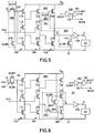
- Figures 5 and 6 show some alternative configurations by way of example and not of limitation. The alternatives are shown as applied to the flip-flop 100. Corresponding alternatives can be applied to the flip-flop 200. The alternative embodiments of the input gate and the output clamp can be applied independently.
- Figure 5 shows an alternative embodiment 340 of the input gate.
- NMOS transistor 345 is connected between ground and the node between the drain of transistor 142 and the gates of transistors 110 and 114.
- the control signal SLON is connected to the gate of transistor 345.
- the control signal SLOFF in its 1 state sets transistor 142 to its ON state and control signal SLON in its 0 state sets transistor 345 to its OFF state.
- the input D is therefore connected to the input stage 102.
- the control signal SLOFF in its 0 state sets transistor 142 to its OFF state and control signal SLON in its 1 state sets transistor 345 to its ON state.
- the input D is therefore isolated from the input stage 102.
- Figure 5 also shows an alternative embodiment 350 of the output clamp.
- the drains of transistors 130 and 134 are directly connected, and the node thus formed provides the output Q-bar.
- the connection between the node formed by the drains of transistors 120 and 122 and the gate of transistor 130 is interrupted by PMOS transistor 352.
- the gate of transistor 352 is connected to receive the control signal SLON.
- the control signal SLON in its 0 state sets transistor 352 to its ON state and sets transistor 154 to its OFF state.
- the state of the output stage 106 therefore depends on the state of the transfer stage 104.
- the control signal SLON in its 1 state sets transistor 352 to its OFF state and sets transistor 154 to its ON state.
- Transistor 154 pulls the output Q-bar to its 0 state, as described above.
- the OFF state of transistor 352 prevents the transistor 130 from pulling the output Q-bar up in conflict with transistor 154.
- Transistor 352 may alternatively interrupt the connection between the source of transistor 130 and the positive supply V DD .
- Figure 6 also shows another alternative embodiment 450 of the output clamp.
- the transistor 454 is connected between the positive supply V DD and the gate of transistor 134.
- the connection between the node formed by the source of transistor 122 and the drain of transistor 124 and the gate of transistor 134 is interrupted by PMOS transistor 456.
- the gate of transistor 456 is connected to receive the control signal SLON.
- the control signal SLON in its 0 state sets transistor 152 to its ON state, as described above, sets transistor 454 to its OFF state and sets transistor 456 to its ON state.
- the state of the output stage 106 therefore depends on the state of the transfer stage 104.
- the control signal SLON in its 1 state sets transistor 152 to its OFF state, as described above, and sets transistor 456 to its OFF state. This disconnects transistor 134 from the transfer stage 104 and from transistor 130 of the output stage.
- the control signal SLON in its 1 state additionally sets transistor 454 to its ON state.
- Transistor 454 in its ON state feeds a clamp signal to the gate of transistor 134.
- the clamp signal causes transistor 134 to pull the output Q-bar down to its 0 state.
- Transistor 152 may alternatively interrupt the connection between the source of transistor 130 and the positive supply V DD .
- the invention has been described above with reference to an example in which a single flip-flop according to the invention sets circuitry to a sleep mode in which the leakage power consumption of the circuitry is less than if the output of the flip-flop were in its other state.
- multiple flip-flops according to the invention some of which have their output Q set to the 1 state in the sleep mode, as in the embodiment 100, others of which their output Q set to the 0 state in the sleep mode, as in the embodiment 200, may have their outputs connected to the circuitry.
- the flip-flops when in their sleep mode, collectively generate a low leakage power vector that sets the circuitry to a sleep mode in which the leakage power consumption of the circuitry is substantially reduced, and is preferably minimized.
- the invention is described above with reference to examples of flip-flops having specific logic states, transistor conduction polarities and supply polarities. However, these are not critical to the invention.
- the invention extends to flip-flops having various combinations of logic states, transistor conduction polarities and supply polarities different from those shown.
Landscapes
- Physics & Mathematics (AREA)
- Engineering & Computer Science (AREA)
- Computer Hardware Design (AREA)
- Computing Systems (AREA)
- General Engineering & Computer Science (AREA)
- Mathematical Physics (AREA)
- Logic Circuits (AREA)
Abstract
Description
| Number & Name | Trans. Count | Ptotal (µW) | Pleak (nW) | CLK-Q Delay (ps) | PDPtot (aJ) | |
| DATA=0 | DATA=1 | |||||
| 1. | 21 | 10.13 | 31.2 | 23.5 | 151 | 1534 |
| 2. | 22 | 15.08 | 35.1 | 27.7 | 162 | 2449 |
| 3. Modified CCMOS | 24 | 9.40 | 9.9 | 10.5 | 184 | 1730 |
| 4. SDFF | 23 | 31.99 | 19.1 | 21.9 | 138 | 4424 |
| 5. | 20 | 14.03 | 2.0 | 3.8 | 108 | 1517 |
| 6. PTTFF | 18 | 12.53 | 18.8 | 18.6 | 166 | 2079 |
| 7. DSTC | 14 | 16.67 | 1.5 | 1.5 | 73 | 1210 |
| 8 | 10 | 2.78 | 0.2 | 4.8 | 146 | 406 |
| 9. 9TDFF | 11 | 2.69 | 4.2 | 3.9 | 132 | 354 |
| 10. HighSpeed DFF | 9 | 216.70 | 463800.0 | 409400.0 | 81 | 17606 |
| 11. | 20 | 8.00 | 2.6 | 1.2 | 166 | 1327 |
| 12. TILPDFF | 18 | 223.60 | 180800.0 | 199500.0 | 93 | 20809 |
| 13. | 22 | 6.72 | 1.2 | 2.8 | 213 | 1433 |
| 14. | 20 | 5.22 | 0.8 | 0.8 | 184 | 960 |
| 15.TSPCFF | 26 | 7.64 | 2.1 | 1.9 | 241 | 1838 |
| 16. | 20 | 6.23 | 1.1 | 2.7 | 235 | 1463 |
| Embodiment 100(1) | 18 | 3.27 | 0.7 | 7.6 | 203 | 664 |
| Embodiment 100(2) | 18 | 1.97 | 0.1 | 5.4 | 203 | 401 |
| Embodiment 200(1) | 18 | 2.99 | 2.8 | 5.1 | 180 | 537 |
| Embodiment 200(2) | 18 | 1.64 | 0.1 | 5.4 | 180 | 295 |
Claims (16)
- A flip-flop having a sleep mode in which power consumption is reduced, the power consumption including leakage power consumption, the flip-flop comprising:a clock input;a data input;an input stage;an input gate interposed between the data input and the input stage and operating in the sleep mode to isolate the input stage from the data input;an output stage coupled to the input stage, the output stage including an output having a first output state and a second output state;output clamp means, operating in the sleep mode, for setting the output to a predetermined state regardless of data states at the data input and the clock input, the predetermined state being the one of the output states in which the leakage power consumption is less than in the other of the output states.
- The flip-flop of claim 1, in which:in the sleep mode, the third transistor is OFF and the fourth transistor is ON.the output stage includes a first transistor of a first conductivity type in series with a second transistor of a second conductivity type;the output clamp means includes:a third transistor of the first conductivity type interposed between the first transistor and the second transistor, anda fourth transistor of the second conductivity type connected in parallel with the second transistor; and
- The flip-flop of claim 1 or 2, in which:the input gate includes a first transistor of a first conductivity type connected in parallel with a second transistor of a second conductivity type, the transistors being interposed between the data input and the input stage; andthe first and second transistors are turned OFF in the sleep mode.
- The flip-flop of one of the preceding claims, in which the output clamp means is configured to feed a clamp signal into the output stage to set the output to the predetermined state.
- The flip-flop of one of the preceding claims, in which the output means is additionally for preventing contention between the predetermined state and the other of the output states when the other of the output states corresponds to the data state at the data input.
- A digital electronic circuit comprising the flip-flop of one of the preceding claims, the digital electronic circuit having a power consumption, including leakage power consumption, the power consumption of the digital electronic circuit being reduced in the sleep mode, in which:the digital electronic circuit comprises circuitry coupled to the output of the flip-flop; andthe predetermined state is the one of the output states in which the leakage power consumption of the digital electronic circuit is less than in the other of the output states.
- The digital electronic circuit of claim 6, in which the predetermined state is the one of the output states in which the leakage power consumption of only the circuitry is less than in the other of the output states.
- The digital electronic circuit of claim 6, in which the predetermined state is the one of the output states in which a sum of the leakage power consumption of the circuitry and the leakage power consumption of the flip-flop is less than in the other of the output states.
- A digital electronic circuit having a sleep mode in which power consumption is reduced, the electronic circuit comprising a data input and a flip-flop according to one of claims 1-5.
- The digital electronic circuit of claim 9, in which:the digital electronic circuit additionally comprises circuitry coupled to the output, the circuitry having leakage power consumption; andthe predetermined state is the one of the output states in which only the leakage power consumption of the circuitry is less than in the other.
- The digital electronic circuit of claim 9, in which:the flip-flop has leakage power consumption; andthe predetermined state is the one of the output states in which only the leakage power consumption of the flip-flop is less than in the other.
- A method of establishing, in a digital electronic circuit, a sleep mode in which power consumption is reduced, the power consumption including leakage power consumption, the digital electronic circuit including a data input and a flip-flop coupled to the data input, the flip flop having a clock input and a data output, the method comprising, in the sleep mode:isolating the data input from the flip flop; andsetting the data output to a predetermined state regardless of data states at the data input and the clock input, the predetermined state being a state of the data output in which the leakage power consumption is reduced.
- The method of claim 12, in which:the electronic circuit additionally includes circuitry connected to the data output, the circuitry having leakage power consumption; andin setting the data output to a predetermined state, the predetermined state is a state in which the leakage power consumption only of the circuitry is reduced.
- The method of claim 12, in which:the flip-flop has leakage power consumption; andin setting the data output to a predetermined state, the predetermined state is a state in which a sum of the leakage power consumption of the circuitry and the leakage power consumption of the flip-flop is reduced.
- The method of claim 12, in which:the flip-flop has leakage power consumption; andin setting the data output to a predetermined state, the predetermined state is a state in which only the leakage power consumption of the flip-flop is reduced.
- The method of one of claims 11-15, in which:the digital electronic circuit includes a plurality of data inputs and a flip-flop coupled to each of the data inputs, each of the flip-flops having a clock input and a data output;in isolating the data input, the each of the data inputs is isolated from the corresponding one of the flip-flops; andin setting the data output, the data output of each of the flip-flops is set to a predetermined state regardless of the data states at the corresponding data input and the clock input to generate, from the predetermined states of the outputs of the flip-flops, a low leakage power vector that reduces the leakage power consumption.
Applications Claiming Priority (2)
| Application Number | Priority Date | Filing Date | Title |
|---|---|---|---|
| US09/655,206 US6275083B1 (en) | 2000-09-05 | 2000-09-05 | Low operational power, low leakage power D-type flip-flop |
| US655206 | 2000-09-05 |
Publications (2)
| Publication Number | Publication Date |
|---|---|
| EP1187328A2 true EP1187328A2 (en) | 2002-03-13 |
| EP1187328A3 EP1187328A3 (en) | 2004-05-12 |
Family
ID=24627956
Family Applications (1)
| Application Number | Title | Priority Date | Filing Date |
|---|---|---|---|
| EP01116203A Withdrawn EP1187328A3 (en) | 2000-09-05 | 2001-07-04 | Low operational power, low leakage power D-type flip-flop |
Country Status (3)
| Country | Link |
|---|---|
| US (1) | US6275083B1 (en) |
| EP (1) | EP1187328A3 (en) |
| JP (1) | JP2002111453A (en) |
Families Citing this family (16)
| Publication number | Priority date | Publication date | Assignee | Title |
|---|---|---|---|---|
| US6693468B2 (en) | 2001-06-12 | 2004-02-17 | Rf Micro Devices, Inc. | Fractional-N synthesizer with improved noise performance |
| US7003049B2 (en) * | 2001-06-12 | 2006-02-21 | Rf Micro Devices, Inc. | Fractional-N digital modulation with analog IQ interface |
| US6779010B2 (en) | 2001-06-12 | 2004-08-17 | Rf Micro Devices, Inc. | Accumulator with programmable full-scale range |
| US6448831B1 (en) * | 2001-06-12 | 2002-09-10 | Rf Micro Devices, Inc. | True single-phase flip-flop |
| EP1331736A1 (en) * | 2002-01-29 | 2003-07-30 | Texas Instruments France | Flip-flop with reduced leakage current |
| US6998895B2 (en) * | 2002-10-29 | 2006-02-14 | Qualcomm, Incorporated | System for reducing leakage in integrated circuits during sleep mode |
| CN100372232C (en) * | 2002-10-29 | 2008-02-27 | 高通股份有限公司 | System for Reducing Leakage in Integrated Circuits |
| KR100519787B1 (en) * | 2002-11-07 | 2005-10-10 | 삼성전자주식회사 | Mtcmos flip-flop circuit capable of retaining data in sleep mode |
| US7085942B2 (en) * | 2003-05-21 | 2006-08-01 | Agilent Technologies, Inc. | Method and apparatus for defining an input state vector that achieves low power consumption in a digital circuit in an idle state |
| US6917662B2 (en) * | 2003-09-11 | 2005-07-12 | International Business Machines Corporation | Programmable low-power high-frequency divider |
| JP4637512B2 (en) * | 2003-11-13 | 2011-02-23 | ルネサスエレクトロニクス株式会社 | Semiconductor integrated circuit device |
| US8421502B2 (en) * | 2005-11-10 | 2013-04-16 | Intel Corporation | Power reducing logic and non-destructive latch circuits and applications |
| JP2007235739A (en) * | 2006-03-02 | 2007-09-13 | Sony Corp | Dynamic flip-flop circuit |
| TWI324856B (en) * | 2006-10-30 | 2010-05-11 | Ind Tech Res Inst | Dynamic floating input d flip-flop |
| US9590602B2 (en) | 2014-06-13 | 2017-03-07 | Stmicroelectronics International N.V. | System and method for a pulse generator |
| TWI756964B (en) * | 2020-12-03 | 2022-03-01 | 智原科技股份有限公司 | D flip-flop |
Family Cites Families (6)
| Publication number | Priority date | Publication date | Assignee | Title |
|---|---|---|---|---|
| US4112296A (en) * | 1977-06-07 | 1978-09-05 | Rockwell International Corporation | Data latch |
| US5789956A (en) | 1995-05-26 | 1998-08-04 | Texas Instruments Incorporated | Low power flip-flop |
| WO1997007592A1 (en) * | 1995-08-14 | 1997-02-27 | Philips Electronics N.V. | Mos master-slave flip-flop with reduced number of pass gates |
| US5774005A (en) * | 1995-09-11 | 1998-06-30 | Advanced Micro Devices, Inc. | Latching methodology |
| JP3230655B2 (en) * | 1996-06-17 | 2001-11-19 | 日本電気株式会社 | Dynamic latch circuit and flip-flop circuit |
| KR100246194B1 (en) | 1997-11-19 | 2000-03-15 | 김영환 | High-speed motion flip flip flop |
-
2000
- 2000-09-05 US US09/655,206 patent/US6275083B1/en not_active Expired - Fee Related
-
2001
- 2001-07-04 EP EP01116203A patent/EP1187328A3/en not_active Withdrawn
- 2001-08-22 JP JP2001251387A patent/JP2002111453A/en active Pending
Also Published As
| Publication number | Publication date |
|---|---|
| EP1187328A3 (en) | 2004-05-12 |
| US6275083B1 (en) | 2001-08-14 |
| JP2002111453A (en) | 2002-04-12 |
Similar Documents
| Publication | Publication Date | Title |
|---|---|---|
| US6275083B1 (en) | Low operational power, low leakage power D-type flip-flop | |
| US7652513B2 (en) | Slave latch controlled retention flop with lower leakage and higher performance | |
| US7750680B2 (en) | Automatic extension of clock gating technique to fine-grained power gating | |
| US7639056B2 (en) | Ultra low area overhead retention flip-flop for power-down applications | |
| EP1510006B1 (en) | Non-volatile multi-threshold cmos latch with leakage control | |
| US7977972B2 (en) | Ultra-low power multi-threshold asynchronous circuit design | |
| US5552738A (en) | High performance energy efficient push pull D flip flop circuits | |
| US7154317B2 (en) | Latch circuit including a data retention latch | |
| Chung et al. | A comparative analysis of low-power low-voltage dual-edge-triggered flip-flops | |
| US9876486B2 (en) | Clock gated flip-flop | |
| Suzuki et al. | A 300 MIPS/W RISC core processor with variable supply-voltage scheme in variable threshold-voltage CMOS | |
| US20180167058A1 (en) | Clock gating cell for low setup time for high frequency designs | |
| TW201123731A (en) | Leakage current reduction in a sequential circuit | |
| US8994406B2 (en) | Digital cell | |
| Lin et al. | Fine-grained power gating for leakage and short-circuit power reduction by using asynchronous-logic | |
| Nagarajan et al. | Power energy and power area product simulation analysis of master-slave flip-flop | |
| Patel et al. | Comparative analysis of adiabatic logic techniques | |
| Gupta et al. | Comparative analysis of single-phase-clocked low power flip-flops with transmission-gate flip-flop | |
| Kaur et al. | Optimization of cmos 8-bit counter using sla and clock gating technique | |
| Smith et al. | Low-Power NCL Design | |
| Akl et al. | Reducing wakeup latency and energy of MTCMOS circuits via keeper insertion | |
| Srikantam et al. | Comparative analysis of flip-flops and application of data-gating in dynamic flip-flops for high speed, low active and low leakage power dissipation | |
| Andrawes et al. | Muli-threshold low power shift register | |
| Gomathi et al. | Design and Speed Analysis of Low Power Single and Double Edge Triggered Flip Flop with Pulse Signal Feed-Through Scheme | |
| Singh et al. | A high performance flip flop for low power low voltage systems |
Legal Events
| Date | Code | Title | Description |
|---|---|---|---|
| PUAI | Public reference made under article 153(3) epc to a published international application that has entered the european phase |
Free format text: ORIGINAL CODE: 0009012 |
|
| AK | Designated contracting states |
Kind code of ref document: A2 Designated state(s): AT BE CH CY DE DK ES FI FR GB GR IE IT LI LU MC NL PT SE TR |
|
| AX | Request for extension of the european patent |
Free format text: AL;LT;LV;MK;RO;SI |
|
| PUAL | Search report despatched |
Free format text: ORIGINAL CODE: 0009013 |
|
| AK | Designated contracting states |
Kind code of ref document: A3 Designated state(s): AT BE CH CY DE DK ES FI FR GB GR IE IT LI LU MC NL PT SE TR |
|
| AX | Request for extension of the european patent |
Extension state: AL LT LV MK RO SI |
|
| RIC1 | Information provided on ipc code assigned before grant |
Ipc: 7H 03K 19/00 B Ipc: 7H 03K 3/356 A |
|
| 17P | Request for examination filed |
Effective date: 20040915 |
|
| AKX | Designation fees paid |
Designated state(s): DE FR GB |
|
| RAP1 | Party data changed (applicant data changed or rights of an application transferred) |
Owner name: AGILENT TECHNOLOGIES, INC. |
|
| GRAP | Despatch of communication of intention to grant a patent |
Free format text: ORIGINAL CODE: EPIDOSNIGR1 |
|
| STAA | Information on the status of an ep patent application or granted ep patent |
Free format text: STATUS: THE APPLICATION IS DEEMED TO BE WITHDRAWN |
|
| 18D | Application deemed to be withdrawn |
Effective date: 20071017 |