EP1187056A2 - Capacitive finger detection for fingerprint sensor - Google Patents
Capacitive finger detection for fingerprint sensor Download PDFInfo
- Publication number
- EP1187056A2 EP1187056A2 EP01306972A EP01306972A EP1187056A2 EP 1187056 A2 EP1187056 A2 EP 1187056A2 EP 01306972 A EP01306972 A EP 01306972A EP 01306972 A EP01306972 A EP 01306972A EP 1187056 A2 EP1187056 A2 EP 1187056A2
- Authority
- EP
- European Patent Office
- Prior art keywords
- detection device
- finger
- frequency
- fingerprint detection
- capacitive
- Prior art date
- Legal status (The legal status is an assumption and is not a legal conclusion. Google has not performed a legal analysis and makes no representation as to the accuracy of the status listed.)
- Granted
Links
Images


Classifications
-
- G—PHYSICS
- G06—COMPUTING OR CALCULATING; COUNTING
- G06V—IMAGE OR VIDEO RECOGNITION OR UNDERSTANDING
- G06V40/00—Recognition of biometric, human-related or animal-related patterns in image or video data
- G06V40/10—Human or animal bodies, e.g. vehicle occupants or pedestrians; Body parts, e.g. hands
- G06V40/12—Fingerprints or palmprints
- G06V40/13—Sensors therefor
- G06V40/1306—Sensors therefor non-optical, e.g. ultrasonic or capacitive sensing
-
- G—PHYSICS
- G06—COMPUTING OR CALCULATING; COUNTING
- G06V—IMAGE OR VIDEO RECOGNITION OR UNDERSTANDING
- G06V40/00—Recognition of biometric, human-related or animal-related patterns in image or video data
- G06V40/40—Spoof detection, e.g. liveness detection
Definitions
- the present invention relates to fingerprint detection and recognition and in particular to finger detection within integrated circuit devices employed for fingerprint-based identification and security mechanisms.
- Fingerprint detection and recognition has become a widely implemented identification and security (verification) measure for a variety of applications, including credit card usage, governmental licensing and registration, and premises access control.
- Integrated circuit fingerprint sensors used in such detection usually contain a two-dimensional array of sensing electrodes at a pitch substantially smaller than the size of the lines on the skin surface of a fingertip, allowing an image of the fingerprint pattern to be acquired for processing, analysis and comparison.
- Fingerprint sensor 402 includes a planar array of sensing electrodes 404 conductively coupled to detection and image capture circuitry (not shown) .
- Sensing electrodes 404 may be covered by a protective layer 406 against which the skin surface 408 of the fingertip is placed. Ridges 410 and valleys 412 formed by the lines on the fingertip skin surface 408 are then detected utilizing sensing electrodes 404 .
- Fingerprint detection is most commonly achieved at least partially through capacitive coupling with the finger.
- skin surface 408 and sensing electrodes 404 each form a capacitor having a capacitance proportional to the distance between a respective sensing electrode 404 and the overlying skin surface 408.
- the capacitance measured by sensor 402 at a point near the top of a fingerprint ridge 410 by a sensing electrode separated from skin surface 408 by a distance d x,y (where x and y denote the position of the respective sensing electrode within the two-dimensional sensor array) will differ from the capacitance measured through another sensing electrode at a point near the bottom of a fingerprint valley 412, where the intervening distance d x,y+2 is greater. In this manner an electronic image of the fingerprint may be captured for further processing.
- Fingerprint detection normally involves a relative or comparative process, in which a characteristic such as capacitance) at one sensing electrode within the array is processed relative to similar measurements by the other sensing electrodes.
- the fingerprint sensor is subject to attack by "spoofing," or presentation of the appropriate fingerprint pattern by an unauthorized individual.
- spoofing or presentation of the appropriate fingerprint pattern by an unauthorized individual.
- the simplest spoofing technique might involve use of a finger severed from an authorized individual for that purpose.
- finger detection is provided by a capacitive grid overlying the fingerprint sensor electrodes to measure the absolute capacitance of the finger placed on the sensor surface.
- the capacitive measurement is converted to a representative frequency, which is then compared to a reference frequency or frequency range to determine whether the measured capacitance matches the expected bio-characteristics of living skin tissue.
- the finger detection thus provides anti-spoofing protection for the fingerprint detection device.
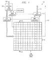
- Figure 1 depicts a block diagram of the sensor circuit 102 , which is formed as an integrated circuit on a single die.
- a suitable sensor circuit 102 and its operation are described more fully in commonly assigned, copending application serial no. 09/040,261, entitled “CAPACITIVE DISTANCE SENSOR” and filed May 9, 1998, which is incorporated herein by reference.
- Sensor circuit 102 includes I 2 C interface and control device 104 , which provides a bidirectional communication protocol enabling sensor circuit 102 to communicate with a controller, such as a microcontroller. I 2 C interface and control device 104 exchanges digital signals via control line 106 with controller circuitry (not shown) external to sensor circuit 102 in the example illustrated, although alternatively such control circuitry may also be integrated within sensor circuit 102 .
- Sensor circuit 102 also includes an array 108 of capacitive sensors for fingerprint acquisition by sensing distances between capacitive electrodes within the sensor array 108 and ridges and grooves on a finger placed in contact with sensor array 108 .
- Sensor array 108 is coupled to the external controller circuit via synchronization line 110 .
- sensor array 108 provides synchronization signals allowing detected voltages representative of the capacitive value of individual capacitive electrodes within sensor array 108 , and therefore representative of the distance between the capacitive electrode and the portion of the epidermal layer contacting sensor array 108 in the region of the capacitive electrode, to be properly interpreted by the external controller.
- Sensor circuit 102 also includes an analog-to-digital (A/D) converter 112 processing analog voltage measurements received from sensor array 108 and generating digital representations recognized by the external controller as distance measurements of the analog measured voltages from individual capacitive electrodes within sensor array 108.
- A/D converter 112 transmits these digital signals to the external controller on output bus 114 .
- Sensor array 108 includes a plurality of cells 116 each containing one or more capacitive electrodes.
- Sensor array 108 in the exemplary embodiment contains square cells approximately 45-50 ⁇ m on a side, forming a 250 X 350 array of contiguous cells 116 within sensor array 108.
- Sensor array 108 is covered by a passivation material overlying the capacitive electrodes within each cell 118 .
- Other active devices required to form sensor circuit 102 are formed below the capacitive electrodes.
- FIGS. 2A through 2C cross-sections of sensor arrays including capacitive finger detection in accordance with a preferred embodiment of the present invention are illustrated.
- the cross-section depicted in Figures 2A and 2B are cross-sections of sensor array 108 taken at section line A-A depicted in Figure 1.
- Cells 116 within sensor array 108 each include at least one capacitive fingerprint sensor electrode 202, which is employed to detect the fingerprint in accordance with the known art.
- a protective layer 204 which may be a combination of insulating and passivating layers, overlies the fingerprint sensor electrodes 202 and provides a surface on which the finger is placed.
- sensor array 108 also includes an array of finger detection sensor electrodes 206a-206c .
- Finger detection sensor electrodes 206a-206c are employed to sense the overall capacitance of the finger when placed on the surface of the sensor array 108. This overall capacitance is then compared to a predefined "sample” or threshold value or range. If the capacitance of the finger is greater than the predefined value (or within the range), a finger is detected on the surface of sensor array 108 .
- Capacitive fingerprint sensor electrodes 202 could be utilized for measuring total capacitance of the finger as well as localized capacitance for detecting fingerprint lines. However, such a design would unnecessarily complicate calculation of capacitances. Instead, separate sensor electrodes 206a-206c , distinct from the capacitive fingerprint sensor electrodes 202 employed to detect the fingerprint, should preferably be employed for capacitive finger detection in accordance with the present invention. Finger detection sensor electrodes may replace the fingerprint detection sensor electrode within a particular cell, as illustrated by sensor electrode 206a , or may be situated between fingerprint detection sensor electrodes 202 , as illustrated by sensor electrode 206b .
- a separate, isolated capacitive grid 206b is formed over the fingerprint sensor detection electrodes 202 .
- Grid lines for the capacitive sensor grid 206b may be formed within the protective layer 204 over spaces between fingerprint sensor detection electrodes 202 as shown in Figure 2A .
- a single capacitive plate 206d may be formed within the protective layer 204 as shown in Figure 2B or above the protective layer 204 as shown in Figure 2C, serving as the capacitive grid. Placement of the finger directly on capacitive plate 206d will still provide a capacitance for measurement and comparison.
- finger detection circuit 302 finger detection sensor electrode(s) 206a or 206d , capacitive grid 206b or capacitive plate 206d (capacitive plate 206d in the example shown) are coupled to a capacitance-to-frequency converter 304.
- the absolute capacitance of a finger placed on the sensor device 102 is measured and utilized to detect a finger.
- This absolute capacitance will depend on the geometry of the contact area and on the bio-characteristics of the skin on the finger. The impact of differing contact geometries may be minimized by limited the size of the finger detection capacitive grid to an area which will normally be completely covered by the finger.
- the impact of the bio-characteristics of the finger for a living person are employed to prevent spoofing by determining whether the finger placed on the fingerprint sensor device 102 provides a capacitance within a predefined range or above a predefined value.
- the capacitance measurement is accomplished by connecting the variable capacitance representing the finger detection electrode 206d and the finger to a capacitance-to-frequency converter 304 , which generates different frequencies depending upon the value of the capacitance measured.
- the frequency output of converter 304 which is a function of the capacitance being measured, is compared to at least one fixed-value reference frequency generated by a stable oscillator 306 .
- the difference in frequencies is determined by a frequency comparator 308 , which generates an output signal 310 indicated whether a finger has been detected.
- the measured capacitance may be compared to absolute thresholds or ranges for the entire populace, or to specific ranges for particular individuals identified by their fingerprint, with the individual ranges of authorized individuals being dynamically updated over time to accommodate aging and seasonal variations in the relevant bio-characteristics.
- fingerprint acquisition by the fingerprint sensor may also be concurrently triggered by the finger detection mechanism of the present invention.
- the present invention employs measurement of bio-characteristics of skin, specifically absolute capacitance of a finger placed on a sensor for fingerprint detection, to provide anti-spoofing protection and real finger detection. Other bio-characteristics of living skin tissue may also be employed in conjunction with the present invention.
- the capacitive finger detection mechanism may be combined with the resistive finger detection mechanism described in the related application, either utilizing separate capacitive and resistive grids or utilizing a single grid for both capacitive and resistive measurements.
Landscapes
- Engineering & Computer Science (AREA)
- Human Computer Interaction (AREA)
- Physics & Mathematics (AREA)
- General Physics & Mathematics (AREA)
- Multimedia (AREA)
- Theoretical Computer Science (AREA)
- Measurement Of The Respiration, Hearing Ability, Form, And Blood Characteristics Of Living Organisms (AREA)
- Measurement Of Length, Angles, Or The Like Using Electric Or Magnetic Means (AREA)
- Image Input (AREA)
Abstract
Description
Claims (15)
- A method of finger detection, comprising:measuring a capacitance between a capacitive grid within a fingerprint detection device and a finger placed on a surface of the fingerprint detection device, wherein the capacitive grid is independent from capacitive sensor electrodes employed within the fingerprint detection device to detect fingerprint features;converting the measured capacitance to a corresponding, representative frequency; andcomparing the frequency representing the measured capacitance to a frequency range corresponding to living skin tissue to determine whether a finger has been placed on the surface of the fingerprint detection device.
- The method of claim 1, wherein the step of measuring a capacitance between a capacitive grid within a fingerprint detection device and a finger placed on a surface of the fingerprint detection device further comprises:measuring the capacitance at a capacitive grid over the capacitive sensor electrodes.
- The method of claim 1, wherein the step of measuring a capacitance between a capacitive grid within a fingerprint detection device and a finger placed on a surface of the fingerprint detection device further comprises:measuring the capacitance at a capacitive grid on the surface of the fingerprint detection device.
- The method of claim 1, wherein the step of comparing the frequency representing the measured capacitance to a frequency range corresponding to living skin tissue to determine whether a finger has been placed on the surface of the fingerprint detection device further comprises:comparing the frequency representing the measured capacitance to a frequency range corresponding to capacitive bio-characteristics of living skin tissue.
- The method of claim 1, wherein the step of comparing the frequency representing the measured capacitance to a frequency range corresponding to living skin tissue to determine whether a finger has been placed on the surface of the fingerprint detection device further comprises:comparing the frequency representing the measured capacitance to a threshold frequency; anddetermining that a finger has been placed on the surface of the fingerprint detection device if the frequency representing the measured capacitance exceeds the threshold frequency.
- The method of claim 1, wherein the step of comparing the frequency representing the measured capacitance to a frequency range corresponding to living skin tissue to determine whether a finger has been placed on the surface of the fingerprint detection device further comprises:comparing the frequency representing the measured capacitance to a predefined frequency range; anddetermining that a finger has been placed on the surface of the fingerprint detection device if the frequency representing the measured capacitance falls within the predefined frequency range.
- The method of claim 1, further comprising:generating a signal indicating whether a finger has been placed on the surface of the fingerprint detection device.
- Anti-spoofing protection for a fingerprint detection device, comprising:a capacitive grid independent from capacitive sensor electrodes employed within the fingerprint detection device to detect fingerprint features;a capacitance-to-frequency converter detecting a capacitance between the capacitive grid and a finger on a surface of the fingerprint detection device and generating a corresponding, representative frequency; anda frequency comparator comparing the frequency representing the capacitance to a frequency range corresponding to capacitive bio-characteristics of living skin tissue to determine whether a finger has been placed on the surface of the fingerprint detection device.
- A fingerprint detection device, comprising:capacitive sensor electrodes employed to detect fingerprint features;a capacitive grid between the capacitive sensor electrodes and a surface of the fingerprint detection device on which a finger is placed for detection of a fingerprint;a capacitance-to-frequency converter converting a capacitance between the capacitive grid and a finger on the surface of the fingerprint detection device into a corresponding, representative frequency; anda frequency comparator comparing the frequency representing the capacitance to a frequency range corresponding to capacitive bio-characteristics of living skin tissue to determine whether a finger has been placed on the surface of the fingerprint detection device.
- The protection or device of claim 8 or 9, wherein the capacitive grid is between the capacitive sensor electrodes and the surface of the fingerprint detection device.
- The protection or device of claim 8 or 9, wherein the capacitive grid is on the surface of the fingerprint detection device.
- The protection or device of claim 8 or 9, further comprising:an oscillator generating at least one reference voltage employed by the frequency comparator to determine whether a finger has been placed on the surface of the fingerprint detection device.
- The protection or device of claim 8 or 9, wherein the oscillator generates a threshold frequency defining a minimum frequency corresponding to converted capacitive bio-characteristics of living skin tissue.
- The protection or device of claim 8 or 9, wherein the oscillator generates a pair of frequencies defining a frequency range corresponding to converted capacitive bio-characteristics of living skin tissue.
- The protection or device of claim 8 or 9, wherein the frequency comparator generates a signal indicating whether a finger has been placed on the surface of the fingerprint detection device.
Applications Claiming Priority (2)
| Application Number | Priority Date | Filing Date | Title |
|---|---|---|---|
| US09/648,968 US6501284B1 (en) | 2000-08-28 | 2000-08-28 | Capacitive finger detection for fingerprint sensor |
| US648968 | 2000-08-28 |
Publications (3)
| Publication Number | Publication Date |
|---|---|
| EP1187056A2 true EP1187056A2 (en) | 2002-03-13 |
| EP1187056A3 EP1187056A3 (en) | 2004-11-17 |
| EP1187056B1 EP1187056B1 (en) | 2006-11-15 |
Family
ID=24602957
Family Applications (1)
| Application Number | Title | Priority Date | Filing Date |
|---|---|---|---|
| EP01306972A Expired - Lifetime EP1187056B1 (en) | 2000-08-28 | 2001-08-16 | Capacitive finger detection for fingerprint sensor |
Country Status (4)
| Country | Link |
|---|---|
| US (1) | US6501284B1 (en) |
| EP (1) | EP1187056B1 (en) |
| JP (1) | JP2002112980A (en) |
| DE (1) | DE60124470T2 (en) |
Cited By (7)
| Publication number | Priority date | Publication date | Assignee | Title |
|---|---|---|---|---|
| FR2849244A1 (en) * | 2002-12-20 | 2004-06-25 | Sagem | Fingerprint sensor has electrodes for determining whether an object placed on it is a living finger or an imitation, with the impedance between the electrodes having to conform to a function relating to the electrode area covered |
| US7612354B2 (en) | 2002-03-19 | 2009-11-03 | Casio Computer Co., Ltd. | Image reading apparatus and drive control method thereof |
| WO2015088436A1 (en) | 2013-12-12 | 2015-06-18 | Fingerprint Cards Ab | Fingerprint sensing system and method comprising a reference sensing element |
| CN105488464A (en) * | 2015-11-26 | 2016-04-13 | 小米科技有限责任公司 | Fingerprint identification method and fingerprint identification apparatus |
| WO2016133602A1 (en) * | 2015-02-20 | 2016-08-25 | Qualcomm Incorporated | Interactive touchscreen and sensor array |
| WO2017058082A1 (en) * | 2015-10-02 | 2017-04-06 | Fingerprint Cards Ab | Method and fingerprint sensing device with finger lost detection |
| WO2017058081A1 (en) * | 2015-10-02 | 2017-04-06 | Fingerprint Cards Ab | Method and device for detecting if a finger is present and sensing a fingerprint pattern |
Families Citing this family (28)
| Publication number | Priority date | Publication date | Assignee | Title |
|---|---|---|---|---|
| US6665428B1 (en) * | 2000-08-28 | 2003-12-16 | Stmicroelectronics, Inc. | Resistive finger detection for fingerprint sensor |
| US6693441B2 (en) * | 2001-11-30 | 2004-02-17 | Stmicroelectronics, Inc. | Capacitive fingerprint sensor with protective coating containing a conductive suspension |
| KR100964559B1 (en) * | 2003-04-25 | 2010-06-21 | 삼성전자주식회사 | Fingerprint reader |
| US20040229681A1 (en) * | 2003-05-12 | 2004-11-18 | Romano James P. | Apparatus and method for generating numbers |
| US7474772B2 (en) | 2003-06-25 | 2009-01-06 | Atrua Technologies, Inc. | System and method for a miniature user input device |
| JP4157557B2 (en) * | 2003-08-15 | 2008-10-01 | 日本電信電話株式会社 | Biological recognition device |
| US7587072B2 (en) | 2003-08-22 | 2009-09-08 | Authentec, Inc. | System for and method of generating rotational inputs |
| CN100374815C (en) * | 2003-08-26 | 2008-03-12 | 日本电信电话株式会社 | Surface Shape Recognition Sensing Device |
| JP4105725B2 (en) * | 2003-08-26 | 2008-06-25 | 日本電信電話株式会社 | Surface shape recognition sensor device |
| WO2005069212A1 (en) * | 2004-01-13 | 2005-07-28 | Fujitsu Limited | Authenticator using organism information |
| US7697729B2 (en) | 2004-01-29 | 2010-04-13 | Authentec, Inc. | System for and method of finger initiated actions |
| US7034552B2 (en) * | 2004-02-17 | 2006-04-25 | Markus Kirchner | Operator sensing circuit for disabling motor of power equipment |
| US7116091B2 (en) * | 2004-03-04 | 2006-10-03 | Zircon Corporation | Ratiometric stud sensing |
| US7148703B2 (en) * | 2004-05-14 | 2006-12-12 | Zircon Corporation | Auto-deep scan for capacitive sensing |
| US7831070B1 (en) | 2005-02-18 | 2010-11-09 | Authentec, Inc. | Dynamic finger detection mechanism for a fingerprint sensor |
| US7738681B1 (en) | 2005-11-01 | 2010-06-15 | Hewlett-Packard Development Company, L.P. | Fingerprint and physical attribute detection |
| US20090278655A1 (en) * | 2008-05-06 | 2009-11-12 | The Abraham Joshua Heschel School | Method for inhibiting egress from a chamber containing contaminants |
| US8149001B2 (en) * | 2008-08-15 | 2012-04-03 | Standard Microsystems Corporation | Low cost fingerprint sensor system |
| DE102009029021B4 (en) * | 2009-08-31 | 2022-09-22 | Robert Bosch Gmbh | Sensor system for monitoring the surroundings of a mechanical component and a method for controlling and evaluating the sensor system |
| US8421890B2 (en) | 2010-01-15 | 2013-04-16 | Picofield Technologies, Inc. | Electronic imager using an impedance sensor grid array and method of making |
| US8791792B2 (en) | 2010-01-15 | 2014-07-29 | Idex Asa | Electronic imager using an impedance sensor grid array mounted on or about a switch and method of making |
| US8866347B2 (en) | 2010-01-15 | 2014-10-21 | Idex Asa | Biometric image sensing |
| US20120092294A1 (en) | 2010-10-18 | 2012-04-19 | Qualcomm Mems Technologies, Inc. | Combination touch, handwriting and fingerprint sensor |
| WO2013155224A1 (en) | 2012-04-10 | 2013-10-17 | Picofield Technologies Inc. | Biometric sensing |
| US9024910B2 (en) | 2012-04-23 | 2015-05-05 | Qualcomm Mems Technologies, Inc. | Touchscreen with bridged force-sensitive resistors |
| WO2015101266A1 (en) * | 2013-12-30 | 2015-07-09 | Byd Company Limited | Sensor for detecting fingerprint and fingerprint identification apparatus and controlling method of sensor for detecting fingerprint |
| US9864895B1 (en) * | 2016-07-07 | 2018-01-09 | Fingerprint Cards Ab | Fingerprint sensing system with finger detect |
| US10102411B2 (en) * | 2017-01-25 | 2018-10-16 | Synaptics Incorporated | Hybrid optical and capacitive sensor |
Family Cites Families (16)
| Publication number | Priority date | Publication date | Assignee | Title |
|---|---|---|---|---|
| FR2386811A1 (en) * | 1977-04-06 | 1978-11-03 | Elf Aquitaine | SEPARATION LEVEL DETECTOR BETWEEN TWO LIQUIDS |
| GB2009427B (en) * | 1977-12-01 | 1982-06-09 | Smiths Industries Ltd | Capacitance to frequency conversion means |
| US4935207A (en) * | 1986-04-01 | 1990-06-19 | The Johns Hopkins University | Capacitive chemical sensor using an ion exchange surface |
| JPH021243A (en) * | 1988-06-08 | 1990-01-05 | Nec Corp | Fake fingerprint detection method and device |
| TW241352B (en) * | 1994-03-30 | 1995-02-21 | Whitaker Corp | Reflective mode ultrasonic touch sensitive switch |
| HU214533B (en) * | 1995-10-06 | 1998-03-30 | Dermo Corporation Ltd. | Detector for identifying living character of a finger |
| US6016355A (en) * | 1995-12-15 | 2000-01-18 | Veridicom, Inc. | Capacitive fingerprint acquisition sensor |
| US6114862A (en) * | 1996-02-14 | 2000-09-05 | Stmicroelectronics, Inc. | Capacitive distance sensor |
| JP3620558B2 (en) * | 1996-12-16 | 2005-02-16 | ソニー株式会社 | Living body detection device |
| JP2962274B2 (en) * | 1997-04-18 | 1999-10-12 | 日本電気株式会社 | Biological identification method and device |
| US5953441A (en) * | 1997-05-16 | 1999-09-14 | Harris Corporation | Fingerprint sensor having spoof reduction features and related methods |
| JP4013089B2 (en) * | 1997-10-23 | 2007-11-28 | ソニー株式会社 | Fingerprint verification device |
| JPH11185020A (en) * | 1997-12-25 | 1999-07-09 | Glory Ltd | Individual authentication sensor |
| DE19830830C2 (en) * | 1998-07-09 | 2000-11-23 | Siemens Ag | Process for the live detection of human skin |
| DE19836770C1 (en) * | 1998-08-13 | 2000-04-20 | Siemens Ag | Capacitive image capture method |
| JP2000172833A (en) * | 1998-12-10 | 2000-06-23 | Omron Corp | Fingerprint collation device |
-
2000
- 2000-08-28 US US09/648,968 patent/US6501284B1/en not_active Expired - Lifetime
-
2001
- 2001-08-16 DE DE60124470T patent/DE60124470T2/en not_active Expired - Lifetime
- 2001-08-16 EP EP01306972A patent/EP1187056B1/en not_active Expired - Lifetime
- 2001-08-28 JP JP2001257286A patent/JP2002112980A/en active Pending
Cited By (12)
| Publication number | Priority date | Publication date | Assignee | Title |
|---|---|---|---|---|
| US7612354B2 (en) | 2002-03-19 | 2009-11-03 | Casio Computer Co., Ltd. | Image reading apparatus and drive control method thereof |
| FR2849244A1 (en) * | 2002-12-20 | 2004-06-25 | Sagem | Fingerprint sensor has electrodes for determining whether an object placed on it is a living finger or an imitation, with the impedance between the electrodes having to conform to a function relating to the electrode area covered |
| WO2004061757A1 (en) * | 2002-12-20 | 2004-07-22 | Sagem S.A. | Method of determining the living character of an element bearing a fingerprint |
| WO2015088436A1 (en) | 2013-12-12 | 2015-06-18 | Fingerprint Cards Ab | Fingerprint sensing system and method comprising a reference sensing element |
| CN105993019A (en) * | 2013-12-12 | 2016-10-05 | 指纹卡有限公司 | Fingerprint sensing system and method comprising a reference sensing element |
| EP3080753A4 (en) * | 2013-12-12 | 2017-08-09 | Fingerprint Cards AB | Fingerprint sensing system and method comprising a reference sensing element |
| WO2016133602A1 (en) * | 2015-02-20 | 2016-08-25 | Qualcomm Incorporated | Interactive touchscreen and sensor array |
| WO2017058082A1 (en) * | 2015-10-02 | 2017-04-06 | Fingerprint Cards Ab | Method and fingerprint sensing device with finger lost detection |
| WO2017058081A1 (en) * | 2015-10-02 | 2017-04-06 | Fingerprint Cards Ab | Method and device for detecting if a finger is present and sensing a fingerprint pattern |
| CN105488464A (en) * | 2015-11-26 | 2016-04-13 | 小米科技有限责任公司 | Fingerprint identification method and fingerprint identification apparatus |
| US10169634B2 (en) | 2015-11-26 | 2019-01-01 | Xiaomi Inc. | Method, device and computer-readable storage medium for fingerprint recognition |
| CN105488464B (en) * | 2015-11-26 | 2019-02-19 | 小米科技有限责任公司 | Fingerprint identification method and device |
Also Published As
| Publication number | Publication date |
|---|---|
| DE60124470T2 (en) | 2007-03-01 |
| DE60124470D1 (en) | 2006-12-28 |
| EP1187056B1 (en) | 2006-11-15 |
| JP2002112980A (en) | 2002-04-16 |
| US6501284B1 (en) | 2002-12-31 |
| EP1187056A3 (en) | 2004-11-17 |
Similar Documents
| Publication | Publication Date | Title |
|---|---|---|
| EP1187056B1 (en) | Capacitive finger detection for fingerprint sensor | |
| US6665428B1 (en) | Resistive finger detection for fingerprint sensor | |
| EP1567057B1 (en) | Live finger detection by four-point measurement of complex impedance | |
| US7642894B2 (en) | Personal identification apparatus using measured tactile pressure | |
| US6597945B2 (en) | Method for detecting living human skin | |
| US6333989B1 (en) | Contact imaging device | |
| US6759264B2 (en) | Pressure type fingerprint sensor fabrication method | |
| US7508963B2 (en) | Surface shape recognition sensor device | |
| US7194113B2 (en) | Capacitive biometric sensor | |
| US20080166028A1 (en) | Pressure actuated biometric sensor | |
| US20080069412A1 (en) | Contoured biometric sensor | |
| JP2010515185A (en) | Personal recognition method and apparatus | |
| WO2004023999A1 (en) | Biosensing instrument and method and identifying device having biosensing function | |
| CN110325951A (en) | Classification method and fingerprint sensing system are touched according to the finger of finger pressure | |
| US10621323B2 (en) | Biometric authentication apparatus and method | |
| US7567690B2 (en) | Method of determining the living character of an element carrying a fingerprint | |
| WO2018226140A1 (en) | Fingerprint authentication method and system for rejecting spoof attempts | |
| US20040125990A1 (en) | Method and apparatus for asperity detection | |
| EP3616123A1 (en) | Fingerprint authentication system and method providing for reduced latency | |
| US20230230410A1 (en) | Fingerprint sensing system and method using thresholding | |
| JPH0981727A (en) | Personal authentication device | |
| KR100641103B1 (en) | Impedance conversion type fingerprint recognition sensor and manufacturing method thereof | |
| KR102335842B1 (en) | Micro sweat detection method and bio-andauthenticating apparatus using the same | |
| Machida et al. | Fingerprint sensor LSI | |
| KR20030093841A (en) | System and Method of Finger-print Recognition |
Legal Events
| Date | Code | Title | Description |
|---|---|---|---|
| PUAI | Public reference made under article 153(3) epc to a published international application that has entered the european phase |
Free format text: ORIGINAL CODE: 0009012 |
|
| AK | Designated contracting states |
Kind code of ref document: A2 Designated state(s): AT BE CH CY DE DK ES FI FR GB GR IE IT LI LU MC NL PT SE TR |
|
| AX | Request for extension of the european patent |
Free format text: AL;LT;LV;MK;RO;SI |
|
| PUAL | Search report despatched |
Free format text: ORIGINAL CODE: 0009013 |
|
| AK | Designated contracting states |
Kind code of ref document: A3 Designated state(s): AT BE CH CY DE DK ES FI FR GB GR IE IT LI LU MC NL PT SE TR |
|
| AX | Request for extension of the european patent |
Extension state: AL LT LV MK RO SI |
|
| 17P | Request for examination filed |
Effective date: 20050506 |
|
| AKX | Designation fees paid |
Designated state(s): DE FR GB IT |
|
| RAP1 | Party data changed (applicant data changed or rights of an application transferred) |
Owner name: UPEK INC., |
|
| GRAP | Despatch of communication of intention to grant a patent |
Free format text: ORIGINAL CODE: EPIDOSNIGR1 |
|
| GRAS | Grant fee paid |
Free format text: ORIGINAL CODE: EPIDOSNIGR3 |
|
| GRAA | (expected) grant |
Free format text: ORIGINAL CODE: 0009210 |
|
| AK | Designated contracting states |
Kind code of ref document: B1 Designated state(s): DE FR GB IT |
|
| REG | Reference to a national code |
Ref country code: GB Ref legal event code: FG4D |
|
| REF | Corresponds to: |
Ref document number: 60124470 Country of ref document: DE Date of ref document: 20061228 Kind code of ref document: P |
|
| EN | Fr: translation not filed | ||
| EN | Fr: translation not filed | ||
| RAP2 | Party data changed (patent owner data changed or rights of a patent transferred) |
Owner name: UPEK, INC. |
|
| PLBE | No opposition filed within time limit |
Free format text: ORIGINAL CODE: 0009261 |
|
| STAA | Information on the status of an ep patent application or granted ep patent |
Free format text: STATUS: NO OPPOSITION FILED WITHIN TIME LIMIT |
|
| 26N | No opposition filed |
Effective date: 20070817 |
|
| ET | Fr: translation filed | ||
| REG | Reference to a national code |
Ref country code: FR Ref legal event code: EERR Free format text: CORRECTION DE BOPI 07/26 - BREVETS EUROPEENS DONT LA TRADUCTION N A PAS ETE REMISE A L INPI. IL Y A LIEU DE SUPPRIMER : LA MENTION DE LA NON REMISE. LA REMISE DE LA TRADUCTION EST PUBLIEE DANS LE PRESENT BOPI. |
|
| GBPC | Gb: european patent ceased through non-payment of renewal fee |
Effective date: 20070816 |
|
| REG | Reference to a national code |
Ref country code: FR Ref legal event code: ST Effective date: 20080430 |
|
| PG25 | Lapsed in a contracting state [announced via postgrant information from national office to epo] |
Ref country code: DE Free format text: LAPSE BECAUSE OF NON-PAYMENT OF DUE FEES Effective date: 20080301 |
|
| REG | Reference to a national code |
Ref country code: GB Ref legal event code: S28 |
|
| REG | Reference to a national code |
Ref country code: FR Ref legal event code: RN |
|
| REG | Reference to a national code |
Ref country code: GB Ref legal event code: S28 Effective date: 20080910 |
|
| PG25 | Lapsed in a contracting state [announced via postgrant information from national office to epo] |
Ref country code: FR Free format text: LAPSE BECAUSE OF NON-PAYMENT OF DUE FEES Effective date: 20070831 |
|
| REG | Reference to a national code |
Ref country code: FR Ref legal event code: FC |
|
| REG | Reference to a national code |
Ref country code: FR Ref legal event code: CA |
|
| PG25 | Lapsed in a contracting state [announced via postgrant information from national office to epo] |
Ref country code: GB Free format text: LAPSE BECAUSE OF NON-PAYMENT OF DUE FEES Effective date: 20070816 |
|
| PGRI | Patent reinstated in contracting state [announced from national office to epo] |
Ref country code: DE Effective date: 20081224 |
|
| PGRI | Patent reinstated in contracting state [announced from national office to epo] |
Ref country code: FR Effective date: 20080924 |
|
| PGFP | Annual fee paid to national office [announced via postgrant information from national office to epo] |
Ref country code: IT Payment date: 20100814 Year of fee payment: 10 |
|
| PG25 | Lapsed in a contracting state [announced via postgrant information from national office to epo] |
Ref country code: IT Free format text: LAPSE BECAUSE OF NON-PAYMENT OF DUE FEES Effective date: 20110816 |
|
| REG | Reference to a national code |
Ref country code: GB Ref legal event code: 732E Free format text: REGISTERED BETWEEN 20120913 AND 20120919 |
|
| REG | Reference to a national code |
Ref country code: FR Ref legal event code: TP Owner name: AUTHENTEC, INC., US Effective date: 20121001 |
|
| REG | Reference to a national code |
Ref country code: DE Ref legal event code: R082 Ref document number: 60124470 Country of ref document: DE Representative=s name: SCHWABE SANDMAIR MARX, DE |
|
| REG | Reference to a national code |
Ref country code: DE Ref legal event code: R082 Ref document number: 60124470 Country of ref document: DE Representative=s name: SCHWABE SANDMAIR MARX, DE Effective date: 20130528 Ref country code: DE Ref legal event code: R081 Ref document number: 60124470 Country of ref document: DE Owner name: AUTHENTEC, INC. (N.D.GES.D.STAATES DELAWARE), US Free format text: FORMER OWNER: UPEK, INC., EMERYVILLE, US Effective date: 20130528 Ref country code: DE Ref legal event code: R081 Ref document number: 60124470 Country of ref document: DE Owner name: AUTHENTEC, INC. (N.D.GES.D.STAATES DELAWARE), , US Free format text: FORMER OWNER: UPEK, INC., EMERYVILLE, CALIF., US Effective date: 20130528 Ref country code: DE Ref legal event code: R082 Ref document number: 60124470 Country of ref document: DE Representative=s name: SCHWABE SANDMAIR MARX PATENTANWAELTE RECHTSANW, DE Effective date: 20130528 Ref country code: DE Ref legal event code: R082 Ref document number: 60124470 Country of ref document: DE Representative=s name: BARDEHLE PAGENBERG PARTNERSCHAFT MBB PATENTANW, DE Effective date: 20130528 Ref country code: DE Ref legal event code: R081 Ref document number: 60124470 Country of ref document: DE Owner name: APPLE INC., CUPERTINO, US Free format text: FORMER OWNER: UPEK, INC., EMERYVILLE, CALIF., US Effective date: 20130528 |
|
| REG | Reference to a national code |
Ref country code: FR Ref legal event code: PLFP Year of fee payment: 15 |
|
| REG | Reference to a national code |
Ref country code: FR Ref legal event code: TP Owner name: APPLE INC., US Effective date: 20160531 |
|
| REG | Reference to a national code |
Ref country code: FR Ref legal event code: PLFP Year of fee payment: 16 |
|
| REG | Reference to a national code |
Ref country code: DE Ref legal event code: R082 Ref document number: 60124470 Country of ref document: DE Representative=s name: BARDEHLE PAGENBERG PARTNERSCHAFT MBB PATENTANW, DE Ref country code: DE Ref legal event code: R081 Ref document number: 60124470 Country of ref document: DE Owner name: APPLE INC., CUPERTINO, US Free format text: FORMER OWNER: AUTHENTEC, INC. (N.D.GES.D.STAATES DELAWARE), MELBOURNE, FLA., US |
|
| REG | Reference to a national code |
Ref country code: GB Ref legal event code: 732E Free format text: REGISTERED BETWEEN 20160811 AND 20160817 |
|
| REG | Reference to a national code |
Ref country code: FR Ref legal event code: PLFP Year of fee payment: 17 |
|
| REG | Reference to a national code |
Ref country code: FR Ref legal event code: PLFP Year of fee payment: 18 |
|
| PGFP | Annual fee paid to national office [announced via postgrant information from national office to epo] |
Ref country code: FR Payment date: 20200715 Year of fee payment: 20 Ref country code: GB Payment date: 20200805 Year of fee payment: 20 Ref country code: DE Payment date: 20200804 Year of fee payment: 20 |
|
| REG | Reference to a national code |
Ref country code: DE Ref legal event code: R071 Ref document number: 60124470 Country of ref document: DE |
|
| REG | Reference to a national code |
Ref country code: GB Ref legal event code: PE20 Expiry date: 20210815 |
|
| PG25 | Lapsed in a contracting state [announced via postgrant information from national office to epo] |
Ref country code: GB Free format text: LAPSE BECAUSE OF EXPIRATION OF PROTECTION Effective date: 20210815 |