EP1187044A2 - Optimised production of hardware from source programs involving multiplications - Google Patents
Optimised production of hardware from source programs involving multiplications Download PDFInfo
- Publication number
- EP1187044A2 EP1187044A2 EP01307187A EP01307187A EP1187044A2 EP 1187044 A2 EP1187044 A2 EP 1187044A2 EP 01307187 A EP01307187 A EP 01307187A EP 01307187 A EP01307187 A EP 01307187A EP 1187044 A2 EP1187044 A2 EP 1187044A2
- Authority
- EP
- European Patent Office
- Prior art keywords
- input
- data flow
- multipliers
- width
- output
- Prior art date
- Legal status (The legal status is an assumption and is not a legal conclusion. Google has not performed a legal analysis and makes no representation as to the accuracy of the status listed.)
- Granted
Links
Images



Classifications
-
- G—PHYSICS
- G06—COMPUTING OR CALCULATING; COUNTING
- G06F—ELECTRIC DIGITAL DATA PROCESSING
- G06F30/00—Computer-aided design [CAD]
- G06F30/30—Circuit design
Definitions
- the invention relates a method of compiling a source program to produce hardware.
- High-level synthesis (also referred to as behavioural synthesis, and described in D. Gajski, A. Wu, N. Dutt, and S. Lin. High-level synthesis: introduction to chip and system design. Kluwer Academic Publishers, 1992.), involves automatically compiling a description of the behaviour of a circuit in a language such as Behavioural VHDL, C/C++ or Java down to equivalent register transfer level (RTL for short) code (e.g. K. Nishida, K. Okada, M. Ohnishi, A. Kay, P. Boca, A. Yamada, and T. Kambe. A high-level synthesis method considering synchronous communications between threads. In Proceedings of VLD '99, 1999).
- RTL is data providing a low level description of the desired circuit. Compiling a source program down to RTL code typically involves subjecting it to a number of steps, as follows:
- steps (a) and (b) above correspond to the source-level optimisation stage
- steps (c) to (f) correspond to the high-level synthesis stage.
- a logic-synthesis tool (such as Synopsys' Design Compiler) can then be used to turn the RTL into a gate-level description. From such a description, a chip 10 (Figure 1) can be produced. (Note: not all high-level synthesis systems treat binding, allocation and scheduling as three distinct stages; some of them combine these stages.)
- High-level synthesis systems include the following: Behavioral Compiler, http://www.synopsys.com; FrontierDesign, http://www.frontierd.com; C level Design, http://www.cleveldesign.com; and A. Kay, "Hardware Compiler", UK Patent Application No. 2317245, filed 12 September 1996.
- the multiplication operations are typically homogeneously typed. That is to say, the types (the word "type” in this specification is used to indicate sign and bit width) of the inputs to these operators are the same as the types of the output.
- Compilers for such languages e.g. the Bach compiler A. Yamada, K Nishida, R. Sakurai, A. Kay, T. Nomura, and T. Kambe. "Hardware synthesis with the Bach system".
- insert type casts automatically so that multiplications are homogenous. Users are encouraged to use homogenous operators rather than to optimise their code by hand for performance. This is because homogeneity reduces the complexity of the language, leading to designs that are more likely to be correct. However, the cost one pays is that the design may not be efficient.
- Figure 2 shows the two stages of high-level hardware design to be source-level optimisation followed by high level synthesis. This is then followed by low-level synthesis. Typically some kind of data-flow representation is used between the source level and the first synthesis level, for example CDFG.
- a multiplier takes two integers as its input, and returns their product as its output .
- Multipliers have different implementations depending on whether inputs and output are to be regarded as signed or unsigned integers. There are 8 different cases in all. To simplify matters we consider here a simpler model where all inputs and outputs are unsigned. The specific embodiments described below cover more cases.
- Non-homogeneous multipliers can be of the form p x q ⁇ r where p and q may be different, and unrelated in size to r.
- High-level synthesis systems apply a number of optimisations to designs to reduce their area.
- One such optimisation is replacing power-of-two multiplications by left-shift operations.
- Previous optimisers may perform strength reduction to completely remove a multiplier, but always generate a homogeneous representation to pass to the high-level synthesis stage.
- any particular tool will use type (a) or type (b) but not both.
- the invention provides a method of compiling a source program to produce hardware, including the steps of:
- the invention thus extends the alphabet of possible bound operator types (e.g. add, multiply, subtract etc) available (in high-level synthesis) to include non-homogeneous multipliers in the data-flow representation before high-level synthesis, as well as homogeneous ones, and to minimise the multiplier input and output widths as much as possible at this early stage.
- this source-level information is made available during high-level synthesis, to enable the synthesis of cheaper, faster circuits.
- Multipliers are expensive in hardware and grow quadratically in size, as the bit width increases.
- bit-width optimisation bit-width optimisation
- the high-level synthesiser must be modified so that it is able to share (when convenient) a single bit-width optimised multiplier functional unit amongst several bit-width-optimised abstract multiplier operators.
- two abstract operators are candidates for sharing if they have exactly the same type. (For multipliers this would mean that both input types and output types have to be the same). This may be too restrictive for general circuits, and the preferred embodiment shows a possible extension, allowing more sharing. Sharing actually occurs only if the schedule permits and if the allocator chooses to do it.
- a circuit with a multiplier which is larger than necessary will often be optimised by simple low-level optimisation rules. For example, if a signal known to be 0 is ANDed with another signal the result will always be 0, so the AND gate can be deleted without affecting the behaviour of the circuit, but improving its performance and cost.
- a single multiplier functional unit might be shared by several different abstract operations, each with its own width requirements. The particular calculation is selected by multiplexors controlled by a special control circuit. Placing these multiplexors in the circuit can 'blind' the low-level optimiser so that it cannot detect optimisations which we could see from the source-level perspective to be perfectly valid.
- Multiplexors 62 and 63 act effectively like switches to determine which two inputs are fed to multiplier 64.
- demultiplexor 65 acts like a switch to determine whether the output of multiplier 64 is fed to y or z.
- the switching behaviour of the multiplexors 62 and 63, and demultiplexor 65, are controlled by controller 68. If the left multiplexor 62 selects its left input (register a), then the left input to the multiplier 64 has 8 bits with values which cannot be determined at compile time. If the left multiplexor 62 selects its right input (cast of register b), then at compile time we know that the top 5 bits are 0. This is because type cast 66 changes the 3 bit output of register a to 8 bits.
- the logic optimiser cannot use this information because it does not know whether the left or right input is selected by multiplexor 62. Therefore, the left input to the multiplier 64 cannot be reduced to less than 8 bits. Therefore an 8 x 8 ⁇ 8 multiplier 64 is required.
- allocation may result in the circuit shown in Figure 8.
- the allocator which performs sharing as one of its tasks, took advantage of the extra information about the size of the two bound operators to share them and use a single 3 x 8 ⁇ 8 multiplier. The resulting circuit is therefore smaller.
- the method allows users to write code in an algorithmic language without having to be unduly concerned with how expensive the code will be in hardware.
- Homogeneous operations are generally easier to understand than non-homogenous ones, so there is less chance for the user to make a mistake.
- the invention allows the user to stick with the easier-to-understand language model, but still to generate compact circuits.
- a control and data flow data graph (CDFG for short) consists of nodes and edges. Each abstract operation in the source language has its own kind of node.
- edges are connected together by edges.
- edge There are two kinds of edge: a control edge and a data edge.
- CDFG Compact Graph Graphics
- CDFGs for representing programs before any high-level synthesis is applied. For this reason, we refer to them as pre-synthesis CDFGs.
- the CDFG optimiser (being the software engine which applies CDFG optimisations) is extended by adding some new rules for reducing the widths of the inputs and outputs of multipliers to a minimum.
- Each application of a rule takes a CDFG as input and returns a CDFG as its output.
- the expression x* ( p , q, r, T ) (( T#q)y) is equivalent to (( T #( ⁇ x )) x ) * ( p,q,r, T) (( T#q ) y ), if x has sign T.
- Rules 0 to 3 relate to reducing the widths of inputs.
- T and T' are either U and S or S and U, x and y are both of sign T'.
- This rule removes the casts from the arguments to the multiplier, changes the type of the multiplier from p x q ⁇ r to ( ⁇ x ) x ( ⁇ y ) ⁇ r and inserts a cast to turn the result back into sign T .
- This rule is similar to rule 2, except that the casts are signed and the function ⁇ is used instead of ⁇ .
- the function ⁇ differs from ⁇ in that an extra bit is used if x is unsigned. The extra bit is required, as signed numbers use one bit to store the sign.
- Rules 4 and 5 relate to reducing the widths of the outputs.
- Rule 4 can then be applied.
- the extra cast inserted is cheap in hardware and would be removed by a logic synthesis tool.
- a high-level optimisation could be applied to the pre-synthesis CDFG to remove casts.
- Implementing such an optimisation has another advantage, as discussed in the subsection relating to rules for removing casts.
- Rule 6 relates to simplifying allocation.
- the arguments to multiplication nodes can be swapped so that the width of the first argument is always less than or equal to that of the second. The following rule achieves this:
- the high-level synthesiser is extended by adding rules 7 and 8 for sharing non-homogeneous multiply operators. For example, suppose that in one clock cycle there is a *(3,4,8,U) and in another there is *(3,5,8,U), then both multiply operations can share the same FU, which is at least *(3, 5, 8, U). We will give two examples of these rules. The first rule applies to abstract multiply operations having the same sign:
- CDFG optimiser can be modified to turn signed multipliers into unsigned ones and use rule 7 for all the sharing of multipliers.
- the invention is not just restricted to multiply operators whose inputs and outputs have the same sign.
- the invention can be applied to multiplies whose inputs and output have different signs as follows:
- the source language used to describe hardware has multiplications whose output width is twice that of the input widths.
- the invention can be applied to such multipliers too, as follows:
Landscapes
- Engineering & Computer Science (AREA)
- Computer Hardware Design (AREA)
- Physics & Mathematics (AREA)
- Theoretical Computer Science (AREA)
- Evolutionary Computation (AREA)
- Geometry (AREA)
- General Engineering & Computer Science (AREA)
- General Physics & Mathematics (AREA)
- Devices For Executing Special Programs (AREA)
- Complex Calculations (AREA)
Abstract
- (a)
- carrying out data flow analysis of the source program to produce a data flow representation of the source program, which data flow representation comprises a number of multipliers each arranged to accept first and second input arguments having first and second input bit widths respectively, and to produce an output having an output bit width; and
- (b)
- optimising the data flow representation so that said input bit widths and output bit width are minimised, even if this results in the input bit widths and output bit width not all being the same for some or all of said multipliers.
- (c)
- carrying out high level synthesis on the optimised data flow representation, including sharing functional units, having input and output bit widths, between said multipliers in such a way that the area of silicon required to produce said functional units is minimised, even if this results in said functional unit input and output bit widths not all being the same.
Description
- The invention relates a method of compiling a source program to produce hardware.
- High-level synthesis (also referred to as behavioural synthesis, and described in D. Gajski, A. Wu, N. Dutt, and S. Lin. High-level synthesis: introduction to chip and system design. Kluwer Academic Publishers, 1992.), involves automatically compiling a description of the behaviour of a circuit in a language such as Behavioural VHDL, C/C++ or Java down to equivalent register transfer level (RTL for short) code (e.g. K. Nishida, K. Okada, M. Ohnishi, A. Kay, P. Boca, A. Yamada, and T. Kambe. A high-level synthesis method considering synchronous communications between threads. In Proceedings of VLD '99, 1999). RTL is data providing a low level description of the desired circuit. Compiling a source program down to RTL code typically involves subjecting it to a number of steps, as follows:
- (a) First, the source program has to be turned into an internal representation. There are several such representations to choose from, but typically control and data-flow graphs (CDFGs) (see D. Gajski, A. Wu, N. Dutt, and S. Lin. High-level synthesis: introduction to chip and system design. Kluwer Academic Publishers, 1992.) are used. The CDFG is produced by a process known as data flow analysis. The CDFG nodes which the source-level optimiser produces (see figure 4) are abstract operations which correspond to source-level concepts such as multiplication, shifting, addition, communication and so on. For example, in Figure 4, the boxes with "*" and "+" in them are nodes.
- (b) The CDFG is then optimised. The optimisations, which are performed on the behavioural description, fall into two categories: those known in software compiler technology and those specifically tailored towards hardware. It is prudent to apply as many optimisations as possible before one commits to a particular hardware architecture, as the size (in terms of silicon area, i.e. number of gates) of expensive operations such as multipliers and hardware shifters can be significantly reduced.
- (c) Binding. This maps operations in the CDFGs to possible functional units (FUs for short) which may be required to realise the design in hardware. During binding each abstract operation is assigned an appropriate bound operator. For example an 8-bit abstract add operation may be assigned to an 8-bit adder; it could equally well be assigned to a more general bound operator, such as a combined add/subtract unit.
- (d) Scheduling. This works out in which clock cycle each of the operations in the CDFG is to be performed, subject to constraints such as clock speed and available resources.
- (e) Allocation. This assigns an actual FU to each operation in the CDFG. To minimise the number of FUs used, sharing is carried out. This involves using the same FU for two different operations of the same kind. For example, if in one clock cycle there is a 3 bit add and in another a 6 bit add, a single 6 bit adder FU can be used for both operations. During allocation each bound operator is allocated to a particular instance of a circuit component, called a functional unit. Functional units usually correspond to instantiations of library components in the RTL. There is a notion of a general circuit component, e.g. a multiplier, and the allocator assigns a bound operator to a particular instance of that component. For example, a 3 x 3 → 3 bound multiplier may be allocated to a 3 x 3 → 3 functional unit. Thus a single functional unit in the low-level RTL might be responsible for implementing several of the abstract operations in the optimised CDFG.
- (f) The final stage of high-level synthesis is to generate RTL code from the scheduled CDFG.
-
- Referring to Figure 2, steps (a) and (b) above correspond to the source-level optimisation stage, and steps (c) to (f) correspond to the high-level synthesis stage.
- A logic-synthesis tool (such as Synopsys' Design Compiler) can then be used to turn the RTL into a gate-level description. From such a description, a chip 10 (Figure 1) can be produced. (Note: not all high-level synthesis systems treat binding, allocation and scheduling as three distinct stages; some of them combine these stages.)
- Some examples of high-level synthesis systems include the following: Behavioral Compiler, http://www.synopsys.com; FrontierDesign, http://www.frontierd.com; C level Design, http://www.cleveldesign.com; and A. Kay, "Hardware Compiler", UK Patent Application No. 2317245, filed 12 September 1996.
- In the high-level languages mentioned above, the multiplication operations are typically homogeneously typed. That is to say, the types (the word "type" in this specification is used to indicate sign and bit width) of the inputs to these operators are the same as the types of the output. Compilers for such languages (e.g. the Bach compiler A. Yamada, K Nishida, R. Sakurai, A. Kay, T. Nomura, and T. Kambe. "Hardware synthesis with the Bach system". In ISCAS '99, 1999) insert type casts automatically so that multiplications are homogenous. Users are encouraged to use homogenous operators rather than to optimise their code by hand for performance. This is because homogeneity reduces the complexity of the language, leading to designs that are more likely to be correct. However, the cost one pays is that the design may not be efficient.
- Figure 2 shows the two stages of high-level hardware design to be source-level optimisation followed by high level synthesis. This is then followed by low-level synthesis. Typically some kind of data-flow representation is used between the source level and the first synthesis level, for example CDFG.
- A multiplier takes two integers as its input, and returns their product as its output . Multipliers have different implementations depending on whether inputs and output are to be regarded as signed or unsigned integers. There are 8 different cases in all. To simplify matters we consider here a simpler model where all inputs and outputs are unsigned. The specific embodiments described below cover more cases.
- In previous tools the "alphabet" of possible multipliers available to be synthesised was always of the form (a) r x r → r or (b) r x r → 2r where p x q → r stands for a multiplier whose inputs are of width p and q and whose output is of width r. We call these types (a) and (b) homogeneous multipliers.
- Non-homogeneous multipliers can be of the form p x q → r where p and q may be different, and unrelated in size to r.
- High-level synthesis systems apply a number of optimisations to designs to reduce their area. One such optimisation is replacing power-of-two multiplications by left-shift operations. (A left-shift operation is written using the symbol «.) For example: x * 8 = x « 3. This is known as strength reduction (see G. Micheli. "Synthesis and Optimization of Digital Circuits." McGraw Hill, 1994).
- Strength reduction also applies to multipliers where one of the operands is expressible as the sum or difference of powers of 2. In such cases, the multiplier can be replaced by a sum or difference of two shifts. For example: x * 7 = x « 3 - x. (Note: x = x « 0.)
- Previous optimisers may perform strength reduction to completely remove a multiplier, but always generate a homogeneous representation to pass to the high-level synthesis stage. Typically, any particular tool will use type (a) or type (b) but not both.
- The invention provides a method of compiling a source program to produce hardware, including the steps of:
- (a) carrying out data flow analysis of the source program to produce a data flow representation of the source program, which data flow representation comprises a number of multipliers each arranged to accept first and second input arguments having first and second input bit widths respectively, and to produce an output having an output bit width; and
- (b) optimising the data flow representation so that said input bit widths and output bit width are minimised, even if this results in the input bit widths and output bit width not all being the same for some or all of said multipliers.
- (c) carrying out high level synthesis on the optimised data flow representation, including sharing functional units, having input and output bit widths, between said multipliers in such a way that the area of silicon required to produce said functional units is minimised, even if this results in said functional unit input and output bit widths not all being the same.
-
- The invention thus extends the alphabet of possible bound operator types (e.g. add, multiply, subtract etc) available (in high-level synthesis) to include non-homogeneous multipliers in the data-flow representation before high-level synthesis, as well as homogeneous ones, and to minimise the multiplier input and output widths as much as possible at this early stage. In doing this source-level information is made available during high-level synthesis, to enable the synthesis of cheaper, faster circuits. Multipliers are expensive in hardware and grow quadratically in size, as the bit width increases.
- To apply the invention to a high-level synthesis system, it is necessary to modify the optimiser, in order to produce optimised descriptions; and the high-level synthesiser in order to take advantage of the extra information.
- Because the width, or number of bits in the inputs and outputs of multipliers, can be reduced by the invention, we refer to this technique as bit-width optimisation.
- The high-level synthesiser must be modified so that it is able to share (when convenient) a single bit-width optimised multiplier functional unit amongst several bit-width-optimised abstract multiplier operators. In the simplest case, two abstract operators are candidates for sharing if they have exactly the same type. (For multipliers this would mean that both input types and output types have to be the same). This may be too restrictive for general circuits, and the preferred embodiment shows a possible extension, allowing more sharing. Sharing actually occurs only if the schedule permits and if the allocator chooses to do it.
- Suppose we want to implement an unsigned multiplication abstract operation p x q → r. Generally, the smaller we make p, q and r, the smaller and faster the multiplication circuit can be. Allowing non-homogenous multipliers means that (say) p can be reduced by the optimiser, leaving q and r fixed. As long as p is wide enough to represent the corresponding input value, the result will be correct. Similarly q can be reduced. Finally r can be reduced in case either (1) r is wider than the value required by the next operator in the graph, or (2) the result of the multiplication can be proved to be always small enough to be represented in fewer bits.
- In low-level synthesis, a circuit with a multiplier which is larger than necessary will often be optimised by simple low-level optimisation rules. For example, if a signal known to be 0 is ANDed with another signal the result will always be 0, so the AND gate can be deleted without affecting the behaviour of the circuit, but improving its performance and cost. However, in high level synthesis a single multiplier functional unit might be shared by several different abstract operations, each with its own width requirements. The particular calculation is selected by multiplexors controlled by a special control circuit. Placing these multiplexors in the circuit can 'blind' the low-level optimiser so that it cannot detect optimisations which we could see from the source-level perspective to be perfectly valid.
- An example of this is given in figures 5 and 6.
- Consider Figure 6 (circuit allocation using prior art). Multiplexors 62 and 63 act effectively like switches to determine which two inputs are fed to
multiplier 64. Similarly, demultiplexor 65 acts like a switch to determine whether the output ofmultiplier 64 is fed to y or z. The switching behaviour of themultiplexors demultiplexor 65, are controlled bycontroller 68. If theleft multiplexor 62 selects its left input (register a), then the left input to themultiplier 64 has 8 bits with values which cannot be determined at compile time. If theleft multiplexor 62 selects its right input (cast of register b), then at compile time we know that the top 5 bits are 0. This is because type cast 66 changes the 3 bit output of register a to 8 bits. However, the logic optimiser cannot use this information because it does not know whether the left or right input is selected bymultiplexor 62. Therefore, the left input to themultiplier 64 cannot be reduced to less than 8 bits. Therefore an 8 x 8 → 8multiplier 64 is required. - Alternatively, using the invention, allocation may result in the circuit shown in Figure 8. The allocator, which performs sharing as one of its tasks, took advantage of the extra information about the size of the two bound operators to share them and use a single 3 x 8 → 8 multiplier. The resulting circuit is therefore smaller.
- Bound operators do not actually appear in the figures. Figure 5 is a CDFG before high-level synthesis, and so the *'s are abstract operations. In Figure 6, the * is a functional unit.
- The method allows users to write code in an algorithmic language without having to be unduly concerned with how expensive the code will be in hardware.
- Homogeneous operations are generally easier to understand than non-homogenous ones, so there is less chance for the user to make a mistake. The invention allows the user to stick with the easier-to-understand language model, but still to generate compact circuits.
- Embodiments will now be more particularly described, by way of example only, with reference to the following drawings, in which:
- Figure 1 gives a picture of a chip;
- Figure 2 gives an outline view of high-level design;
- Figure 3 gives a flowchart explaining how the optimisation rules in the embodiment are applied;
- Figure 4 is an example of a CDFG for representing the expression (x * y) + (z * w);
- Figure 5 gives a pre-synthesis CDFG for a small example;
- Figure 6 gives a possible circuit schematic after running the example in Figure 5 through a high level synthesis system;
- Figure 7 gives the CDFG that results from applying the optimisation rules in the embodiment to the CDFG in Figure 5; and
- Figure 8 gives a possible circuit schematic that may result from applying the proposed extension (to a high-level synthesis) to the CDFG in Figure 5.
-
- The following notation will be used in the description.
- (a) U stands for unsigned and S stands for signed. Signed and unsigned are standard ANSI C (see B. W. Kernigan and D. M. Ritchie. "The ANSI C Programming Language". Software Series. Prentice Hall, 1988.) In a signed integer the first bit stands for a negative number, e.g. for the 4 bit case: -8, 4, 2, 1. As an example, the signed 4 bit integer 1100 represents -4 (i.e. -8+4), whereas the unsigned 4 bit integer 1100 represents 12 (i.e. +8+4).
- (b) T and T' will be used to stand for signs, i.e. U or S.
- (c) A p x q → r multiplier, where p and q are less than or equal to r, has inputs of width p and q and output of width r.
- (d) The notation *(p, q, r, T) stands for a p x q → r multiplier of sign T, where T is either U or S.
- (e) unsigned # n is an unsigned type of width n, and signed #n is a signed type of width n.
- (f) σ returns the width of a given expression. For example, if x and y are defined
thus
- unsigned #3 x;
- signed #4 y; then σ x = 3 and σ y = 4. σ can therefore be regarded as a form of shorthand.
- (g) (U # n) x means cast (i.e. change) x to type unsigned #n and (S#n) x means cast x
to type signed #n. If n is smaller than the width of x, x will be truncated. If n is
larger than the width of x, there are two possible outcomes:
- if x is signed, n - σ x copies of the sign bit of x will be joined onto x. This is called sign extension.
- if x is unsigned, n - σ x zeros will be joined onto x.
- (h) └┘ works out the maximum of two numbers. For example └┘ (3, 4) = 4.
-
- The following terminology is also used:
- (a) A homogeneous multiplier of width r is a r x r → r multiplier.
- (b) A non-homogeneous multiplier is a p x q → r multiplier where p and q are less than r.
- (c) An operation is commutative if its arguments can be swapped. Multiplication is commutative. (For example, 5*3 = 3*5.)
- (d) A cast is an operation which changes the type of an integer, and is carried out by a "type cast"
-
- We will present rules in the form

- This is to be read as "if e satisfies p 1, then replace e by f1 ... if e satisfies pk then replace e by f k". We will assume that e can satisfy only one of the conditions.
- Rules for sharing abstract multiply operators will be expressed thus:
- A control and data flow data graph (CDFG for short) consists of nodes and edges. Each abstract operation in the source language has its own kind of node.
- Nodes are connected together by edges. There are two kinds of edge: a control edge and a data edge. We will use a standard form of CDFG, such as the kind described in D. Gajski, A. Wu, N. Dutt, and S. Lin. "High-level synthesis: introduction to chip and system design". Kluwer Academic Publishers, 1992.
- For example, consider the expression (x * y) + (z * w), where x, y, z and w each have the same type. A CDFG representing this expression is given in Figure 4. Notice that each of the operations * and + corresponds to a node (shown as a box). Edges (shown as arrows) lead from x and y into one of the multiplies and edges lead from z and w into the other multiply. The outputs from the multiplies lead into the addition node. These edges are data edges, and show the flow of data through the graph.
- We will use CDFGs for representing programs before any high-level synthesis is applied. For this reason, we refer to them as pre-synthesis CDFGs.
- In the embodiments described here the CDFG optimiser and the high-level synthesis system are extended. These extensions will now be described.
- The CDFG optimiser (being the software engine which applies CDFG optimisations) is extended by adding some new rules for reducing the widths of the inputs and outputs of multipliers to a minimum.
- Each application of a rule takes a CDFG as input and returns a CDFG as its output.
- The rules are to be applied repeatedly (as shown by the flowchart in Figure 3).
- To aid description, we write down the input and output of the rules using horizontal notation. This notation is the expression that the fragment of CDFG represents. In addition, for simplicity, we assume that the rules apply to expressions of the form
- Rules 0 to 3 relate to reducing the widths of inputs.
- where T and T' are either U and S or S and U, x and y are both of sign T'.

- This rule removes the casts from the arguments to the multiplier, changes the type of the multiplier from p x q → r to (σx) x (σy) → r and inserts a cast to turn the result back into sign T.
- where T is either S or U, and the signs of x and y are also T. Here is an explanation of the rule:
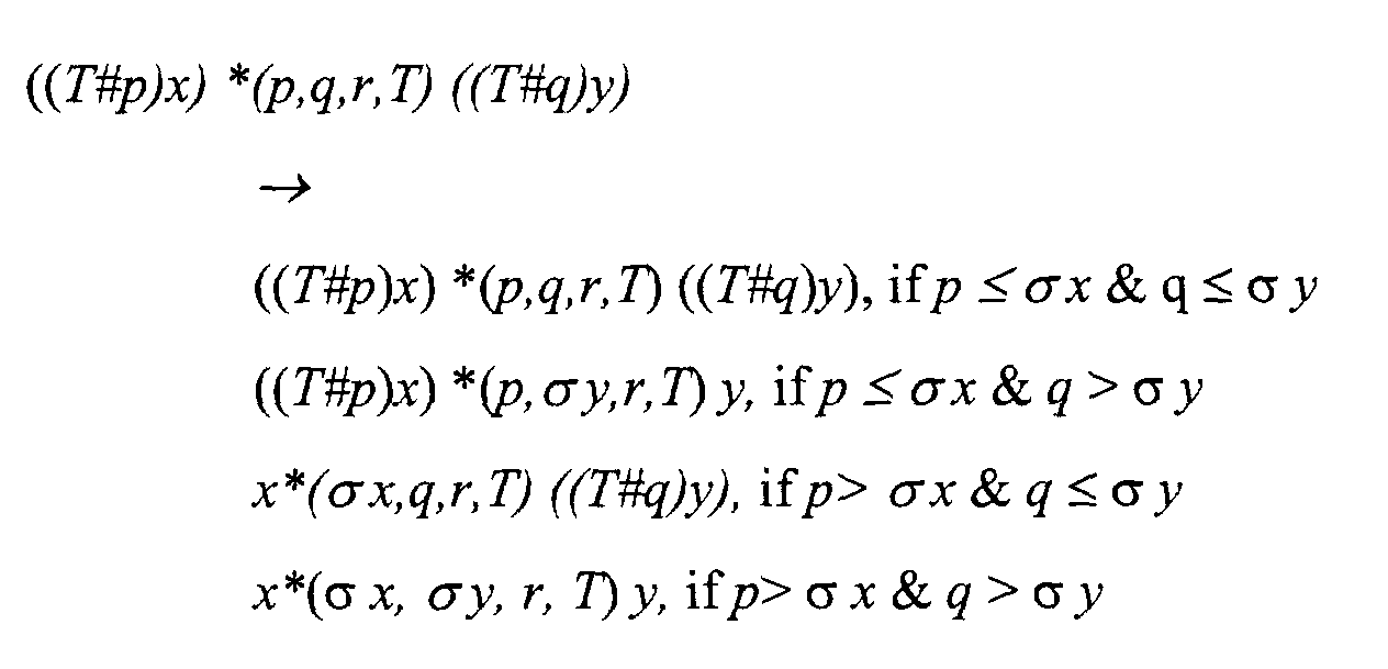
- p ≤ σ x & q ≤ σ y line: says that if p and q are narrower than or equal to the widths of x and y respectively, there is no optimisation to perform.
- p ≤ σ x & q > σ y line: says that if p is not wider than the width of x and q is wider than the width of y then remove the cast from y and change the type of the multiplier to p x (σ y) → r.
- p > σ x & q ≤ σ y line: like the previous line, except that the cast is removed from x and the type of the multiplier is changed to (σ x) x q → r.
- p > σx & q > σy line: says that if p and q are wider than the widths of x and y respectively, both of the casts can be removed and the type of the multiplier changed to (σ x) x (σ y) → r.
-
- where x and y have different signs (i.e. one is signed and the other is unsigned), and is defined thus:
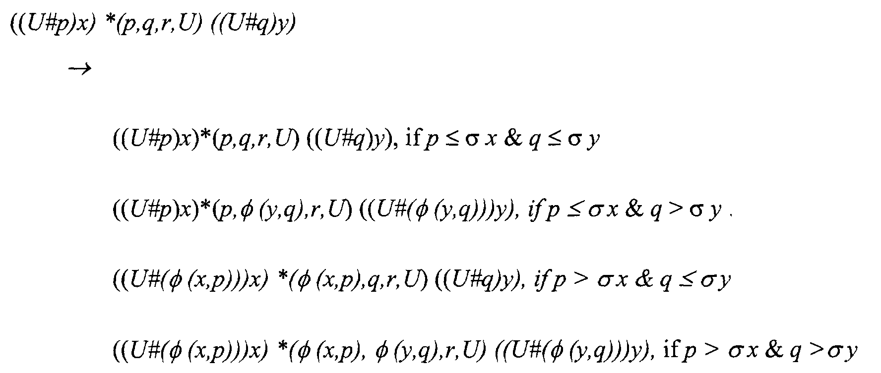
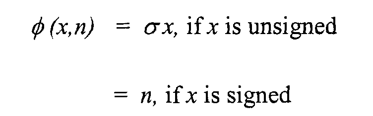
- The function takes an expression x and a number n and returns the width of x if x is unsigned. If x is signed, returns n. We will now explain rule 2:
- if p ≤ σ x & q ≤ σ y line: says that if p and q are narrower than or equal to the widths of x and y respectively, there is no optimisation to perform.
- if p ≤ σ x & q > σ y line: says that if p is not wider than the width of x and q is wider than the width of y, do not change the first argument but replace the second argument with (U#((y,q)))y. The expression that this cast will expand into depends on the sign of q: (U#((y,q)))y expands to (U#(σy))y if y is unsigned and to (U#q)y if y is signed. The type of the multiplier is changed to p x ((y,q)) → r.
- if p > σ x & q ≤ σ y line: This is similar to the previous line, except that the first argument is modified and the multiplier changed to type ((x,p))xq → r.
- if p > σ x & q > σ y line: says that if p and q are wider than the widths of x and y respectively, it may be possible to narrow the widths of x and y. Whether narrowing will occur depends on the signs of x and y. The type of the multiplier is changed to ((x,p)) x ((y,q)) → r
-
- where the signs of x and y are different, and ψ is defined thus:

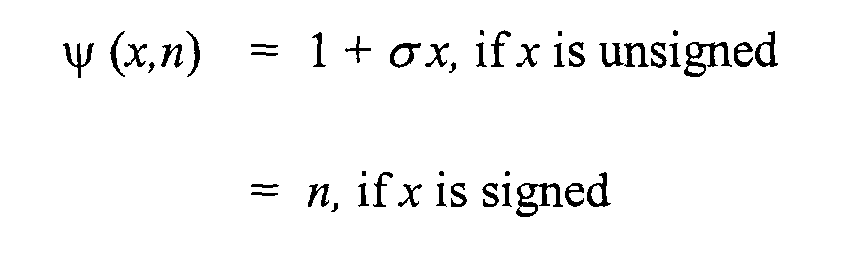
- This rule is similar to rule 2, except that the casts are signed and the function ψ is used instead of . The function ψ differs from in that an extra bit is used if x is unsigned. The extra bit is required, as signed numbers use one bit to store the sign.
- Rules 4 and 5 relate to reducing the widths of the outputs.
- Often in calculations, only some of the bits in the result of a multiplication are needed. This manifests itself in a CDFG as casting the output of a multiplier. We describe some rules that reduce the width of multipliers in this situation. These may introduce the possibility of applying rules 0 to 3 to further bit-width optimise multipliers. Throughout this section, we take T and T' to stand for either U and S, or S and U.
- The first rule we give applies to multipliers whose sign is the same as that of the cast:
-

- We will now explain what this rule does:
- n > r line: if the width of the cast is larger than the output width of the multiplier then leave the expression unchanged.
- The other lines deal with the various cases where it is possible to shrink the output of the multiplier.
- n ≤ r & n < p&n < q line: if the width of the cast is narrower than the widths of the inputs to the multiplier then cast the inputs and change the multiplier to n x n → n.
- n ≤ r & n < p&n ≥ q line: says that if the width of the cast is narrower than the width of the first argument (but not the second), then insert a cast to reduce the width of the first argument and change the type of the multiplier to n x q → n.
- n ≤ r& n ≥ p&n < q line: like the previous line, except that it narrows the second argument (by inserting a type cast), changing the type of the multiplier to p x n → n.
- n ≤ r & n ≥ p & n ≥ q line: says that if n is greater than or equal to both p and q, the cast can be removed and the type of the multiplier changed to p x q → n.
-
- The next rule deals with the case where the sign of the multiplier is different from that of the cast:
-
- Rule 4 can then be applied. The extra cast inserted is cheap in hardware and would be removed by a logic synthesis tool. Alternatively, a high-level optimisation could be applied to the pre-synthesis CDFG to remove casts. Implementing such an optimisation has another advantage, as discussed in the subsection relating to rules for removing casts.
- Rule 6 relates to simplifying allocation.
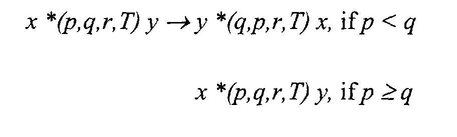
- We can capitalise on the commutivity of multiplication to allow more sharing of functional units. At the pre-binding stage, the arguments to multiplication nodes can be swapped so that the width of the first argument is always less than or equal to that of the second. The following rule achieves this:
-
- Typically in a pre-synthesis CDFG there will be "chains" of casts; that is to say, expressions of the form (T1#n1) ((T2#n2)(...((Tk#nk)x)...)), where k ≥ 2 and the T is are either U or S. The presence of such chains can prevent the application of the rules described for bit-width optimising multipliers. We therefore propose that optimisations for simplifying chains of casts should be incorporated into a CDFG optimiser in known manner.
- The high-level synthesiser is extended by adding
rules 7 and 8 for sharing non-homogeneous multiply operators. For example, suppose that in one clock cycle there is a *(3,4,8,U) and in another there is *(3,5,8,U), then both multiply operations can share the same FU, which is at least *(3, 5, 8, U). We will give two examples of these rules. The first rule applies to abstract multiply operations having the same sign: -
- If one multiplier is signed and the other is unsigned, there is a choice of multiplier functional unit to use. But it is cheaper to use an unsigned FU:
-
- This rule is sound, since unsigned multipliers can be used in place of signed ones (as can easily be proved).
- In an alternative embodiment the CDFG optimiser can be modified to turn signed multipliers into unsigned ones and use rule 7 for all the sharing of multipliers.
- An example will now be given to illustrate the above. The example concerns the following fragment of code:
- unsigned#8 a, d, y, z, w;
- unsigned#3 b, c;
-
- A CDFG representation of this fragment is given in Figure 5. Because the multiply operation is homogeneous, type casts 52 and 54 have had to be inserted to widen b and c to 8 bits. A high-level synthesis system will schedule these operations and perform sharing.
- One possible circuit schematic that could arise by passing this example through a high-level synthesis system is given in Figure 6. (For simplicity, we have ignored the addition.) Notice that in the graph in Figure 6 two
multiplexors width 8. The outputs of thesemultiplexors operation 64. - Now suppose that the invention is applied. Applying optimisation rules1 and 6 to the CDFG in Figure 5 removes the two
casts multiplexors 82 has an output width of 3 and the other 84 has an output width of 8. The outputs from these multiplexors are input into a 3 x 8 → 8 multiplyoperation 80. Multiplexors 82 and 84, and ademultiplexor 86, are controlled by acontroller 88. - As mentioned in Section 5, the invention is not just restricted to multiply operators whose inputs and outputs have the same sign. The invention can be applied to multiplies whose inputs and output have different signs as follows:
- (a) in the pre-synthesis CDFG, apply the optimisations described by the above rules;
- (b) after all of the optimisations have been applied, add another transformation pass to remove unnecessary casts, yielding multiply nodes whose inputs and outputs do not necessarily have the same sign; and
- (c) modify the
sharing rules 7 and 8 accordingly. -
- In some high-level synthesis systems, the source language used to describe hardware has multiplications whose output width is twice that of the input widths. The invention can be applied to such multipliers too, as follows:
- (a) at the pre-synthesis CDFG level, turn r x r → 2r multipliers into r x r → r multipliers;
- (b) apply the optimisation rules described above;
- (c) in a separate transformation pass, turn p x q → r multipliers into p x q → 2r multipliers; and
- (d) use the
sharing rules 7 and 8. -
Claims (7)
- A method of compiling a source program to produce hardware, including the steps of:(a) carrying out data flow analysis of the source program to produce a data flow representation of the source program, which data flow representation comprises a number of multipliers each arranged to accept first and second input arguments having first and second input bit widths respectively, and to produce an output having an output bit width; and(b) optimising the data flow representation so that said input bit widths and output bit width are minimised, even if this results in the input bit widths and output bit width not all being the same for some or all of said multipliers.(c) carrying out high level synthesis on the optimised data flow representation, including sharing functional units, having input and output bit widths, between said multipliers in such a way that the area of silicon required to produce said functional units is minimised, even if this results in said functional unit input and output bit widths not all being the same.
- A method as claimed in claim 1, wherein said data flow representation is a CDFG.
- A method as claimed in claim 1 or 2, wherein at least one of said multipliers in the optimised data flow representation has input bit widths and an output bit width which are not all the same.
- A method as claimed in any preceding claim, wherein each multiplier may be signed or unsigned.
- A method as claimed in claim 1, wherein said optimising step includes applying any of rules 0 to 5 which reduce said input bit width or output bit width.
- A method as claimed in claim 1, wherein said sharing step includes applying rule 6, 7 or 8 which allow sharing of said functional unit.
- A method as claimed in claim 5, wherein said sharing step includes applying rule 6, 7 or 8 which allow sharing of said functional unit.
Applications Claiming Priority (2)
| Application Number | Priority Date | Filing Date | Title |
|---|---|---|---|
| GB0021222 | 2000-08-30 | ||
| GB0021222A GB2366404A (en) | 2000-08-30 | 2000-08-30 | A method for improving the high-level synthesis of expressions involving multiplications |
Publications (3)
| Publication Number | Publication Date |
|---|---|
| EP1187044A2 true EP1187044A2 (en) | 2002-03-13 |
| EP1187044A3 EP1187044A3 (en) | 2002-07-03 |
| EP1187044B1 EP1187044B1 (en) | 2004-03-24 |
Family
ID=9898471
Family Applications (1)
| Application Number | Title | Priority Date | Filing Date |
|---|---|---|---|
| EP01307187A Expired - Lifetime EP1187044B1 (en) | 2000-08-30 | 2001-08-23 | Optimised production of hardware from source programs involving multiplications |
Country Status (5)
| Country | Link |
|---|---|
| US (1) | US6820257B2 (en) |
| EP (1) | EP1187044B1 (en) |
| JP (1) | JP2002149728A (en) |
| DE (1) | DE60102425T2 (en) |
| GB (1) | GB2366404A (en) |
Cited By (1)
| Publication number | Priority date | Publication date | Assignee | Title |
|---|---|---|---|---|
| US10268798B2 (en) | 2015-09-22 | 2019-04-23 | International Business Machines Corporation | Condition analysis |
Families Citing this family (3)
| Publication number | Priority date | Publication date | Assignee | Title |
|---|---|---|---|---|
| US6925628B2 (en) * | 2002-10-22 | 2005-08-02 | Matsushita Electric Industrial Co., Ltd. | High-level synthesis method |
| JP5109764B2 (en) * | 2008-03-31 | 2012-12-26 | 日本電気株式会社 | Description processing apparatus, description processing method, and program |
| US8136063B2 (en) * | 2008-11-14 | 2012-03-13 | Synopsys, Inc. | Unfolding algorithm in multirate system folding |
Family Cites Families (2)
| Publication number | Priority date | Publication date | Assignee | Title |
|---|---|---|---|---|
| US5541849A (en) * | 1990-04-06 | 1996-07-30 | Lsi Logic Corporation | Method and system for creating and validating low level description of electronic design from higher level, behavior-oriented description, including estimation and comparison of timing parameters |
| US5910898A (en) * | 1995-12-14 | 1999-06-08 | Viewlogic Systems, Inc. | Circuit design methods and tools |
-
2000
- 2000-08-30 GB GB0021222A patent/GB2366404A/en not_active Withdrawn
-
2001
- 2001-08-21 US US09/934,080 patent/US6820257B2/en not_active Expired - Fee Related
- 2001-08-23 DE DE60102425T patent/DE60102425T2/en not_active Expired - Lifetime
- 2001-08-23 EP EP01307187A patent/EP1187044B1/en not_active Expired - Lifetime
- 2001-08-29 JP JP2001260404A patent/JP2002149728A/en active Pending
Non-Patent Citations (2)
| Title |
|---|
| KUM K-I ET AL: "Word-length optimization for high-level synthesis of digital signal processing systems" , SIGNAL PROCESSING SYSTEMS, 1998. SIPS 98. 1998 IEEE WORKSHOP ON CAMBRIDGE, MA, USA 8-10 OCT. 1998, NEW YORK, NY, USA,IEEE, US, PAGE(S) 569-578 XP010303719 ISBN: 0-7803-4997-0 * abstract * * page 576, paragraph 1 * * page 577, paragraph 3 * * |
| TOGAWA N ET AL: "A high-level synthesis system for digital signal processing based on enumerating data-flow graphs" , DESIGN AUTOMATION CONFERENCE 1998. PROCEEDINGS OF THE ASP-DAC '98. ASIA AND SOUTH PACIFIC YOKOHAMA, JAPAN 10-13 FEB. 1998, NEW YORK, NY, USA,IEEE, US, PAGE(S) 265-274 XP010275930 ISBN: 0-7803-4425-1 * abstract * * page 265 - page 267 * * |
Cited By (1)
| Publication number | Priority date | Publication date | Assignee | Title |
|---|---|---|---|---|
| US10268798B2 (en) | 2015-09-22 | 2019-04-23 | International Business Machines Corporation | Condition analysis |
Also Published As
| Publication number | Publication date |
|---|---|
| US6820257B2 (en) | 2004-11-16 |
| EP1187044A3 (en) | 2002-07-03 |
| GB2366404A (en) | 2002-03-06 |
| EP1187044B1 (en) | 2004-03-24 |
| DE60102425T2 (en) | 2005-02-24 |
| DE60102425D1 (en) | 2004-04-29 |
| JP2002149728A (en) | 2002-05-24 |
| GB0021222D0 (en) | 2000-10-18 |
| US20020026305A1 (en) | 2002-02-28 |
Similar Documents
| Publication | Publication Date | Title |
|---|---|---|
| US20160299998A1 (en) | Logic circuit generation device and method | |
| EP0829812A2 (en) | Method of designing an integrated circuit and integrated circuit designed by such method | |
| EP1412832A2 (en) | Procedure for optimizing mergeability and datapath widths of data flow graphs | |
| EP1475699B1 (en) | Multiplier | |
| KR960001277B1 (en) | Method of realizing digital signal processors using a programmed | |
| US6604232B2 (en) | High-level synthesis method and storage medium storing the same | |
| US20040237056A1 (en) | Behavioral synthesis system, behavioral synthesis method, control program, readable recording medium, logic circuit production method, and logic circuit | |
| EP1187044B1 (en) | Optimised production of hardware from source programs involving multiplications | |
| US6292926B1 (en) | Functional module model, pipelined circuit synthesis and pipelined circuit device | |
| Bruneel et al. | Dynamic data folding with parameterizable FPGA configurations | |
| US7228531B1 (en) | Methods and apparatus for optimizing a processor core on a programmable chip | |
| Potkonjak et al. | Considering testability at behavioral level: use of transformations for partial scan cost minimization under timing and area constraints | |
| Meredith | High-level SystemC synthesis with forte's cynthesizer | |
| US7509246B1 (en) | System level simulation models for hardware modules | |
| US7729898B1 (en) | Methods and apparatus for implementing logic functions on a heterogeneous programmable device | |
| US6532584B1 (en) | Circuit synthesis method | |
| JP2001209670A (en) | High-level synthesis method and recording medium used for implementing high-level synthesis method | |
| Lanneer et al. | An object-oriented framework supporting the full high-level synthesis trajectory | |
| Berkelaar | Area-power-delay trade-off in logic synthesis | |
| GB2279785A (en) | Designing pipelined stages in a computer-aided design system. | |
| JP3602697B2 (en) | Logic circuit design support system | |
| Benkrid et al. | Efficient FPGA hardware development: A multi-language approach | |
| Monahan et al. | Concurrent analysis techniques for data path timing optimization | |
| Ushenina et al. | Implementing sticky bit generators based on FPGA carry-chains for floating-point adders | |
| Shewring et al. | An integrated approach to the design and implementation of image filters |
Legal Events
| Date | Code | Title | Description |
|---|---|---|---|
| PUAI | Public reference made under article 153(3) epc to a published international application that has entered the european phase |
Free format text: ORIGINAL CODE: 0009012 |
|
| AK | Designated contracting states |
Kind code of ref document: A2 Designated state(s): AT BE CH CY DE DK ES FI FR GB GR IE IT LI LU MC NL PT SE TR |
|
| AX | Request for extension of the european patent |
Free format text: AL;LT;LV;MK;RO;SI |
|
| PUAL | Search report despatched |
Free format text: ORIGINAL CODE: 0009013 |
|
| AK | Designated contracting states |
Kind code of ref document: A3 Designated state(s): AT BE CH CY DE DK ES FI FR GB GR IE IT LI LU MC NL PT SE TR |
|
| AX | Request for extension of the european patent |
Free format text: AL;LT;LV;MK;RO;SI |
|
| 17P | Request for examination filed |
Effective date: 20020821 |
|
| 17Q | First examination report despatched |
Effective date: 20021104 |
|
| AKX | Designation fees paid |
Designated state(s): DE FR GB |
|
| GRAP | Despatch of communication of intention to grant a patent |
Free format text: ORIGINAL CODE: EPIDOSNIGR1 |
|
| GRAS | Grant fee paid |
Free format text: ORIGINAL CODE: EPIDOSNIGR3 |
|
| GRAA | (expected) grant |
Free format text: ORIGINAL CODE: 0009210 |
|
| AK | Designated contracting states |
Kind code of ref document: B1 Designated state(s): DE FR GB |
|
| REG | Reference to a national code |
Ref country code: GB Ref legal event code: FG4D |
|
| REG | Reference to a national code |
Ref country code: IE Ref legal event code: FG4D |
|
| REF | Corresponds to: |
Ref document number: 60102425 Country of ref document: DE Date of ref document: 20040429 Kind code of ref document: P |
|
| ET | Fr: translation filed | ||
| PLBE | No opposition filed within time limit |
Free format text: ORIGINAL CODE: 0009261 |
|
| STAA | Information on the status of an ep patent application or granted ep patent |
Free format text: STATUS: NO OPPOSITION FILED WITHIN TIME LIMIT |
|
| 26N | No opposition filed |
Effective date: 20041228 |
|
| REG | Reference to a national code |
Ref country code: IE Ref legal event code: MM4A |
|
| PGFP | Annual fee paid to national office [announced via postgrant information from national office to epo] |
Ref country code: DE Payment date: 20130821 Year of fee payment: 13 |
|
| PGFP | Annual fee paid to national office [announced via postgrant information from national office to epo] |
Ref country code: GB Payment date: 20130821 Year of fee payment: 13 Ref country code: FR Payment date: 20130808 Year of fee payment: 13 |
|
| REG | Reference to a national code |
Ref country code: DE Ref legal event code: R119 Ref document number: 60102425 Country of ref document: DE |
|
| GBPC | Gb: european patent ceased through non-payment of renewal fee |
Effective date: 20140823 |
|
| REG | Reference to a national code |
Ref country code: DE Ref legal event code: R119 Ref document number: 60102425 Country of ref document: DE Effective date: 20150303 |
|
| REG | Reference to a national code |
Ref country code: FR Ref legal event code: ST Effective date: 20150430 |
|
| PG25 | Lapsed in a contracting state [announced via postgrant information from national office to epo] |
Ref country code: GB Free format text: LAPSE BECAUSE OF NON-PAYMENT OF DUE FEES Effective date: 20140823 Ref country code: DE Free format text: LAPSE BECAUSE OF NON-PAYMENT OF DUE FEES Effective date: 20150303 |
|
| PG25 | Lapsed in a contracting state [announced via postgrant information from national office to epo] |
Ref country code: FR Free format text: LAPSE BECAUSE OF NON-PAYMENT OF DUE FEES Effective date: 20140901 |