EP1186094B1 - Method and apparatus for converting a dc voltage to an ac voltage - Google Patents
Method and apparatus for converting a dc voltage to an ac voltage Download PDFInfo
- Publication number
- EP1186094B1 EP1186094B1 EP00930608A EP00930608A EP1186094B1 EP 1186094 B1 EP1186094 B1 EP 1186094B1 EP 00930608 A EP00930608 A EP 00930608A EP 00930608 A EP00930608 A EP 00930608A EP 1186094 B1 EP1186094 B1 EP 1186094B1
- Authority
- EP
- European Patent Office
- Prior art keywords
- power
- inverter
- voltage source
- load
- voltage
- Prior art date
- Legal status (The legal status is an assumption and is not a legal conclusion. Google has not performed a legal analysis and makes no representation as to the accuracy of the status listed.)
- Expired - Lifetime
Links
Images




Classifications
-
- H—ELECTRICITY
- H02—GENERATION; CONVERSION OR DISTRIBUTION OF ELECTRIC POWER
- H02M—APPARATUS FOR CONVERSION BETWEEN AC AND AC, BETWEEN AC AND DC, OR BETWEEN DC AND DC, AND FOR USE WITH MAINS OR SIMILAR POWER SUPPLY SYSTEMS; CONVERSION OF DC OR AC INPUT POWER INTO SURGE OUTPUT POWER; CONTROL OR REGULATION THEREOF
- H02M7/00—Conversion of AC power input into DC power output; Conversion of DC power input into AC power output
- H02M7/42—Conversion of DC power input into AC power output without possibility of reversal
- H02M7/44—Conversion of DC power input into AC power output without possibility of reversal by static converters
- H02M7/48—Conversion of DC power input into AC power output without possibility of reversal by static converters using discharge tubes with control electrode or semiconductor devices with control electrode
- H02M7/53—Conversion of DC power input into AC power output without possibility of reversal by static converters using discharge tubes with control electrode or semiconductor devices with control electrode using devices of a triode or transistor type requiring continuous application of a control signal
- H02M7/537—Conversion of DC power input into AC power output without possibility of reversal by static converters using discharge tubes with control electrode or semiconductor devices with control electrode using devices of a triode or transistor type requiring continuous application of a control signal using semiconductor devices only, e.g. single switched pulse inverters
- H02M7/5383—Conversion of DC power input into AC power output without possibility of reversal by static converters using discharge tubes with control electrode or semiconductor devices with control electrode using devices of a triode or transistor type requiring continuous application of a control signal using semiconductor devices only, e.g. single switched pulse inverters in a self-oscillating arrangement
- H02M7/53832—Conversion of DC power input into AC power output without possibility of reversal by static converters using discharge tubes with control electrode or semiconductor devices with control electrode using devices of a triode or transistor type requiring continuous application of a control signal using semiconductor devices only, e.g. single switched pulse inverters in a self-oscillating arrangement in a push-pull arrangement
-
- H—ELECTRICITY
- H02—GENERATION; CONVERSION OR DISTRIBUTION OF ELECTRIC POWER
- H02J—ELECTRIC POWER NETWORKS; CIRCUIT ARRANGEMENTS OR SYSTEMS FOR SUPPLYING OR DISTRIBUTING ELECTRIC POWER; SYSTEMS FOR STORING ELECTRIC ENERGY
- H02J9/00—Circuit arrangements for emergency or stand-by power supply, e.g. for emergency lighting
- H02J9/04—Circuit arrangements for emergency or stand-by power supply, e.g. for emergency lighting in which the distribution system is disconnected from the normal source and connected to a standby source
- H02J9/06—Circuit arrangements for emergency or stand-by power supply, e.g. for emergency lighting in which the distribution system is disconnected from the normal source and connected to a standby source with automatic change-over, e.g. UPS systems
- H02J9/062—Circuit arrangements for emergency or stand-by power supply, e.g. for emergency lighting in which the distribution system is disconnected from the normal source and connected to a standby source with automatic change-over, e.g. UPS systems for AC powered loads
-
- Y—GENERAL TAGGING OF NEW TECHNOLOGICAL DEVELOPMENTS; GENERAL TAGGING OF CROSS-SECTIONAL TECHNOLOGIES SPANNING OVER SEVERAL SECTIONS OF THE IPC; TECHNICAL SUBJECTS COVERED BY FORMER USPC CROSS-REFERENCE ART COLLECTIONS [XRACs] AND DIGESTS
- Y02—TECHNOLOGIES OR APPLICATIONS FOR MITIGATION OR ADAPTATION AGAINST CLIMATE CHANGE
- Y02B—CLIMATE CHANGE MITIGATION TECHNOLOGIES RELATED TO BUILDINGS, e.g. HOUSING, HOUSE APPLIANCES OR RELATED END-USER APPLICATIONS
- Y02B70/00—Technologies for an efficient end-user side electric power management and consumption
- Y02B70/10—Technologies improving the efficiency by using switched-mode power supplies [SMPS], i.e. efficient power electronics conversion e.g. power factor correction or reduction of losses in power supplies or efficient standby modes
Definitions
- Embodiments of the present invention are directed generally to a method and an apparatus for converting a DC voltage to an AC voltage. More specifically, embodiments of the present invention are directed to methods and apparatus for converting DC voltages to AC voltages using resonant bridge inverter circuits in devices such as uninterruptible power supplies.
- UPSs uninterruptible power supplies
- Fig. 1 shows a typical prior art UPS 10 used to provide regulated uninterrupted power.
- the UPS 10 includes an input filter/surge protector 12, a transfer switch 14, a controller 16, a battery 18, a battery charger 19, an inverter 20, and a DC-DC converter 23.
- the UPS also includes an input 24 for coupling to an AC power source and an outlet 26 for coupling to a load.
- the UPS 10 operates as follows.
- the filter/surge protector 12 receives input AC power from the AC power source through the input 24, filters the input AC power and provides filtered AC power to the transfer switch and the battery charger.
- the transfer switch 14 receives the AC power from the filter/surge protector 12 and also receives AC power from the inverter 20.
- the controller 16 determines whether the AC power available from the filter/surge protector is within predetermined tolerances, and if so, controls the transfer switch to provide the AC power from the filter/surge protector to the outlet 26. If the AC power from the protector is not within the predetermined tolerances, which may occur because of "brown out,” “high line,” or “black out” conditions, or due to power surges, then the controller controls the transfer switch to provide the AC power from the inverter 20.
- the DC-DC converter 23 is an optional component that converts the output of the battery to a voltage that is compatible with the inverter. Depending on the particular inverter and battery used the inverter may be operatively coupled to the battery either directly or through a DC-DC converter.
- the inverter 20 of the prior art UPS 10 receives DC power from the DC-DC converter 23, converts the DC voltage to AC voltage, and regulates the AC voltage to predetermined specifications.
- the inverter 20 provides the regulated AC voltage to the transfer switch.
- the UPS 10 can provide power to the load during brief power source "dropouts" or for extended power outages.
- a typical prior art inverter circuit 100 is shown in Fig. 2 coupled to a DC voltage source 18a and coupled to a typical load 126 comprising a load resistor 128 and a load capacitor 130.
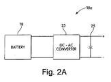
- the DC voltage source 18a may be a battery, or may include a battery 18 coupled to a DC-DC converter 23 and a capacitor 25 as shown in Fig. 2A.
- Typical loads have a capacitive component due to the presence of an EMI filter in the load.
- the inverter circuit 100 includes four switches S1, S2, S3 and S4.
- Each of the switches is implemented using power MOSFET devices which consist of a transistor 106, 112, 118, 124 having an intrinsic diode 104, 110, 116, and 122.
- Each of the transistors 106, 112, 118 and 124 has a gate, respectively 107, 109, 111 and 113.
- each of the switches S1 - S4 can be controlled using a control signal input to its gate.
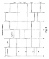
- Fig. 3 provides timing waveforms for the switches to generate an output AC voltage waveform Vout (also shown in Fig. 3) across the capacitor 130 and the resistor 128.
- a major drawback of the prior art inverter circuit 100 is that for loads having a capacitive component, a significant amount of power is dissipated as the load capacitance is charged and discharged during each half-cycle of the AC waveform. This power is absorbed by the switches S1, S2, S3, S4, which typically requires the switches to be mounted to relatively large heat sinks. The power dissipation issue becomes greater for high voltage systems, wherein the energy required to charge the load capacitance is greater. The dissipation of power in the switches dramatically reduces the efficiency of the inverter, and accordingly, reduces the run-time of the battery 18 in the UPS 10. Temperature rise of the switches also becomes a large concern.
- EP-A-0 420 628 discloses an AC to DC to AC power conversion apparatus, with few active switches, for use with single phase UPS systems.
- EP-A-0 696 831 discloses a modular power supply system for providing a multiplicity of output voltages from a plurality of converter modules.
- the problems associated with power dissipation in an inverter due to capacitor charging and discharging are eliminated by providing a resonant circuit in the inverter to charge and discharge the capacitor.
- the present invention features an inverter for an uninterruptible power supply as defined in claim 1.
- the set of switches in the inverter can include a second switch electrically coupled between the second output node and the second input node, a third switch electrically coupled between the second output node and the first input node, a fourth switch electrically coupled between the first output node and the first input node, and a fifth switch electrically coupled between the first output node and the second input node.
- the inverter can further include a sixth switch electrically coupled between the first terminal of the inductive circuit element and the second input node.
- the inductive circuit element in the inverter may include an inductor.
- Each of the switches may include a transistor.
- the energy storage device can include a battery.
- the transfer switch can be constructed and arranged to receive the AC power from the input and to receive the AC power from the inverter and to provide one of the AC power from the input and the AC power from the inverter to the load.
- the present invention features an uninterruptible power supply as defined in claim 9.
- An embodiment of the present invention features an uninterruptible power supply for providing AC power to a load having a capacitive element.
- the uninterruptible power supply includes an input to receive AC power from an AC power source, an output that provides AC power, a voltage source that provides DC power, the voltage source having an energy storage device, an inverter operatively coupled to the voltage source to receive DC power and having an output to provide AC power.
- the inverter includes means for charging the capacitive element by supplying electrical current from the inverter to the load through an inductive circuit element, means for supplying load current from the inverter after the capacitive element has been charged to a predetermined voltage, means for discharging the capacitive element through the inductive circuit element, and means for transferring energy from the inductive circuit element to the energy storage device.
- the uninterruptible power supply further includes a transfer switch constructed and arranged to select one of the AC power source and the voltage source as an output power source for the uninterruptible power supply.
- the present invention features a method of supplying an uninterruptible AC voltage to a load having a capacitive element using an uninterruptible power supply having a DC voltage source with an energy storage device.
- the method includes steps of charging the capacitive element by supplying electrical current from the DC voltage source to the load through an inductive circuit element in the uninterruptible power supply, supplying load current from the DC voltage source to the load after the capacitive element has been charged to a predetermined voltage, discharging the capacitive element through the inductive circuit element, and transferring energy stored in the inductive circuit from the inductive circuit element to the energy storage device in the DC voltage source.
- the method can further include steps of receiving an AC voltage from an AC power source, selecting one of the AC power source and the DC voltage source as an output power source for the uninterruptible power supply.
- the inverter 200 includes MOSFET switches S1, S2, S3 and S4 of the prior art inverter 100 and includes two additional MOSFET switches S5 and S6 and an inductor 140.
- the switches S5 and S6 are similar to switches S1 - S4 and include a transistor 134, 138 having an intrinsic diode 132, 136.
- Each of the transistors 134 and 138 has a gate 115 and 117 that is used to control the state of the transistor.
- the switches S1 - S6 are implemented using part no. IRF640 available from International Rectifier of El Segundo, CA. For 220 VAC applications, the switches may be implemented using part no. IRF730 also available from International Rectifier.
- the inductor 140 in the 120 VAC embodiment, is implemented using a 1.5 mH inductor having a very high Bsat value to be able to withstand high peak currents without saturating. In one embodiment, the inductor is made from an EI lamination structure of M-19, 18.5 mil steel having a large air gap between the E and I laminations.
- inductors may be used with embodiments of the present invention depending upon the peak switch current and physical size of the inductor desired.
- the transition time or time required to charge or discharge the load capacitance, should also be considered to prevent the transition time from becoming either too short or too long. If the transition time is too long, then the pulse width of the output waveform may become too long. If the transition time is too short, the peak switch currents become greater.
- Fig. 5 provides a timing diagram of the operation of the switches S1 - S6 of the inverter 200 and also provides the output voltage waveform across the load 126.
- the switch is turned on (conducting state) and when the corresponding waveform is in the low state the switch is turned off (non-conducting state).
- the switches are shown as being implemented using NMOS devices.
- NMOS complementary metal-oxide-semiconductor
- a control signal having a positive state is supplied to the gate of the device to turn the device on (conducting), while a control signal having a low state is supplied to the gate to turn the device off (non-conducting).
- the timing diagram of each of the switches also represents the state of the control signal provided to the gate of the corresponding transistor.
- the control signals may be provided from, for example, controller 16 of the UPS of Fig. 1 when the inverter is used in a UPS.
- the control signals may be supplied using timing logic circuits residing within the inverter itself as is known in the art.
- switches S4 and S5 are turned on and switches S1, S2, S3 and S6 are turned off creating a current path through the inverter 200 in the direction of arrows 150 as shown in Fig. 6. Only the components of the inverter 200 in the current path created during the first time period are shown in Fig. 6.
- switches S4 and S5 turned on, the inductor 140 and the load 126 are connected in series across the voltage source 18a.
- the output voltage across the load Vout rises in a resonant manner from zero volts to the voltage of the voltage source 18a.
- the output voltage Vout is prevented from rising beyond the voltage of the voltage source by the diode 104 (Fig. 7) of switch S1.
- the diode 104 will conduct current to limit the output voltage Vout to the voltage of the voltage source.
- Fig. 7 shows the current path through the inverter during the second time period. As shown in Fig, 7, load current during the second period follows arrows 154.
- the energy that was stored in the inductor during the first time period causes the voltage across the inductor to reverse and energy in the inductor is released to a storage device in the voltage source, such as a battery or a capacitor, through a current that follows a path along arrow 156 through diode 104 of switch 1 and diode 136 of switch 6.
- a storage device in the voltage source such as a battery or a capacitor
- current from the energy stored in the inductor may also follow a path through the load.
- switch S6 is turned off, and all switches remain off during a fourth time period from t3 until t4.
- the current path through the inverter 200 during the fourth time period follows arrows 160 shown in Fig. 9.
- the energy in the inductor 140 freewheels into the voltage source 18a through diodes 110 and 132 of S2 and S5, and the voltage across the load typically remains at zero.
- the time from t3 until t4 is normally chosen to be long enough to permit all of the inductor energy to be transferred to the voltage source 18a.
- switches S1 and S3 are turned on to maintain a low impedance across the load to prevent any external energy from charging the output to a non-zero voltage. This is referred to as the "clamp" period.
- all switches are again turned off and remain off for a sixth time period until time t6.
- the negative half cycle of the AC waveform is created.
- the negative half cycle is created in substantially the same manner as the positive half cycle described above, except that switch S3 is substituted for switch S4, switch S6 is substituted for S5 and switch S2 is substituted for S1.
- the positive and negative half cycles then continue to be generated in an alternating manner to create an AC output voltage waveform.
- the first time period from t0 to t1 is approximately 130 microseconds
- the second time period from t1 to t2 is approximately 4 milliseconds
- the third time period from t2 to t3 is approximately 130 microseconds
- the fourth time period from t3 to t4 is approximately 100 microseconds
- the time period from time t4 to t5 is approximately 4.2 milliseconds
- the time period from t5 to t6 is approximately 10 microseconds.
- the negative half cycle of the waveform is symmetric with the positive half cycle, and accordingly, the rise time, fall time and duration of the negative half cycle are approximately equal to those of the positive half cycle.
- switches S1 and S3 are turned on to clamp the output to a low impedance.
- switches S2 and S4 are turned on rather than switches S1 and S3.
- switches S1 and S3 are turned on, however, switches S2 and S4 could be turned on in place of switches S1 and S3. Turning on S2 instead of S1 after the positive half cycle is beneficial in that the voltage drop across S2 is lowered, and since switch S2 is in the energy recovery path for inductor 140, the lower voltage drop increases circuit efficiency.
- the inverter 200 is used in the manner described above, to create an output AC voltage having the waveform shown in Fig. 5 from an input DC voltage using a resonance circuit.
- the use of the resonance circuit allows the load capacitance to be charged and discharged with only a minimum power loss.
- the only power losses incurred in the inverter 200 are due to characteristics of inverter components including the ESR of the inductor and due to series resistance of each of the switches when in the on state.
- inverters in accordance with embodiments of the present invention do not require bulky heat sinks like inverters of the prior art, and are more efficient than inverters of the prior art.
- the improved efficiency of inverters in accordance with embodiments of the present invention make them particularly desirable for use in uninterruptible power supplies, wherein they can extend the operating time of a UPS in battery mode, reduce the size and weight of the UPS and reduce electromagnetic emissions from the UPS.
- inverters are described as being used with uninterruptible power supplies, for example, in place of the inverter 20 in the UPS 10 of Fig. 1.
- inverters of the present invention may also be used with other types of uninterruptible power supplies.
- the inverters may be used with UPSs in which an input AC voltage is converted to a DC voltage and one of the converted DC voltage and a DC voltage provided from a battery-powered DC voltage source is provided to an input of the inverter to create the AC output voltage of the UPS.
- UPSs in which an input AC voltage is converted to a DC voltage and one of the converted DC voltage and a DC voltage provided from a battery-powered DC voltage source is provided to an input of the inverter to create the AC output voltage of the UPS.
- inverters in accordance with embodiments of the present invention may also be used in systems and devices other than uninterruptible power supplies.
- MOSFET devices are used as the switches S 1 - S6.
- switches S 1 - S6 a number of other electrical or mechanical switches, such as IGBT's with integral rectifiers, or bipolar transistors having a diode across the C-E junction, may be used to provide the functionality of the switches.
- each of the switches S1 - S6 need not be implemented using the same type of switch.
- an inductor is used as a resonant element in inverter circuits.
- other devices having a complex impedance may be used in place of the inductor, however, it is desirable that any such device be primarily inductive in nature.
- the voltage source may include a battery that receives the energy from the inductor, or the voltage source may include a storage device other than a battery, such as a capacitor, coupled in parallel across the voltage source that receives the energy.
Landscapes
- Engineering & Computer Science (AREA)
- Power Engineering (AREA)
- Business, Economics & Management (AREA)
- Emergency Management (AREA)
- Inverter Devices (AREA)
- Electrical Discharge Machining, Electrochemical Machining, And Combined Machining (AREA)
- Stand-By Power Supply Arrangements (AREA)
Abstract
Description
Claims (12)
- An inverter for providing AC power to a load (126) having a capacitative element (130), comprising input node means to receive DC power from a DC voltage source; output node means to provide AC power to the load (126); and a set of switches (106, 112,118,124) operatively coupled between the output node means and the input node means and actuated in use in a predetermined manner to generate AC power from the DC power; characterised by an inductive circuit element (140) having a first terminal and a second terminal, the second terminal being electrically coupled to the output node means; and switch means (S5,S6) electrically coupled between the first terminal of the circuit element and the input node means, the switch means being cooperatively actuable with the set of switches to transfer energy stored in the capacitative element to the inductive circuit element, and to transfer the energy stored in the inductive circuit element to the input node means for transferring said energy to the DC voltage source coupled to said input node means.
- The inverter of claim 1, wherein the set of switches includes:a switch (S1) electrically coupled between a first output node and a first input node;a switch (S2) electrically coupled between the first output node and a second input node;a switch (S3) electrically coupled between a second output node and the first input node; anda switch (S4) electrically coupled between the second output node and the second input node.
- The inverter of claim 2, wherein the switch means (S5,S6) comprises a switch (S5) electrically coupled between the first terminal of the inductive circuit element (140) and the first input node and a switch (S6) electrically coupled between the first terminal of the inductive circuit element (140) and the second input node.
- The inverter of any preceding claim wherein the DC voltage source comprises an energy storage device, the inverter comprising:means for charging the capacitative element by supplying electrical current from the inverter (200) to the load (126) through the inductive circuit element (140);means for supplying load current from the inverter (200) after the capacitative element (130) has been charged to a predetermined voltage;means for discharging the capacitative element through the inductive circuit element (140); andmeans for transferring energy from the inductive circuit element (140) to the energy storage device (18a).
- The inverter of claim 4, wherein the energy storage device comprises a battery (18a).
- The inverter of any one of claims 1 to 5, wherein each of the switches includes a transistor.
- The inverter of any one of claims 1 to 6, wherein the inductive circuit element comprises an inductor (140).
- The inverter of claim 7, wherein the capacitative element comprises a capacitor.
- An uninterruptible power supply for providing AC power to a load (126) having a capacitative element (130), the uninterruptible power supply comprising:an input (24) to receive AC power from an AC power source (24);an output (26) that provides AC power;a DC voltage source (18a) that provides DC power, the DC voltage source having an energy storage device;the inverter (200) of any one of claims 1 to 8 coupled to the DC voltage source; anda transfer switch (14) constructed and arranged to select one of the AC power source and the inverter as an output power source for the uninterruptible power supply.
- A method of supplying an uninterruptible AC voltage to a load (126) having a capacitative element (130) using an uninterruptible power supply having a DC voltage source with an energy storage device (18a), the method comprising steps of:charging the capacitative element (130) by supplying electrical current from the DC voltage source to the load (126) through an inductive circuit element (140);supplying load current from the DC voltage source to the load after the capacitative element (130) has been charged to a predetermined voltage;discharging the capacitative element (130) via said inductive circuit element (140);storing transitory energy in said inductive circuit element (140) during discharging of the capacitative element; andtransferring energy from said inductive circuit element (140) to the energy storage device (18a).
- The method of claim 10, further comprising steps of:receiving an AC voltage from an AC power source (24);selecting one of the AC power source and the DC voltage source as an output power source for the uninterruptible power supply.
- The method of claim 10 or claim 11, wherein the capacitative element comprises a capacitor and the inductive circuit element comprises an inductor.
Priority Applications (1)
| Application Number | Priority Date | Filing Date | Title |
|---|---|---|---|
| EP20050076944 EP1605577B1 (en) | 1999-05-13 | 2000-05-11 | Method and apparatus for converting a DC voltage to an AC voltage |
Applications Claiming Priority (3)
| Application Number | Priority Date | Filing Date | Title |
|---|---|---|---|
| US311043 | 1981-10-13 | ||
| US09/311,043 US6404658B1 (en) | 1999-05-13 | 1999-05-13 | Method and apparatus for converting a DC voltage to an AC voltage |
| PCT/US2000/012921 WO2000070736A1 (en) | 1999-05-13 | 2000-05-11 | Method and apparatus for converting a dc voltage to an ac voltage |
Related Child Applications (1)
| Application Number | Title | Priority Date | Filing Date |
|---|---|---|---|
| EP20050076944 Division EP1605577B1 (en) | 1999-05-13 | 2000-05-11 | Method and apparatus for converting a DC voltage to an AC voltage |
Publications (2)
| Publication Number | Publication Date |
|---|---|
| EP1186094A1 EP1186094A1 (en) | 2002-03-13 |
| EP1186094B1 true EP1186094B1 (en) | 2005-08-31 |
Family
ID=23205147
Family Applications (2)
| Application Number | Title | Priority Date | Filing Date |
|---|---|---|---|
| EP20050076944 Expired - Lifetime EP1605577B1 (en) | 1999-05-13 | 2000-05-11 | Method and apparatus for converting a DC voltage to an AC voltage |
| EP00930608A Expired - Lifetime EP1186094B1 (en) | 1999-05-13 | 2000-05-11 | Method and apparatus for converting a dc voltage to an ac voltage |
Family Applications Before (1)
| Application Number | Title | Priority Date | Filing Date |
|---|---|---|---|
| EP20050076944 Expired - Lifetime EP1605577B1 (en) | 1999-05-13 | 2000-05-11 | Method and apparatus for converting a DC voltage to an AC voltage |
Country Status (9)
| Country | Link |
|---|---|
| US (4) | US6404658B1 (en) |
| EP (2) | EP1605577B1 (en) |
| JP (1) | JP4651824B2 (en) |
| AT (1) | ATE303668T1 (en) |
| AU (1) | AU770941B2 (en) |
| CA (1) | CA2373762C (en) |
| DE (1) | DE60022346T2 (en) |
| ES (1) | ES2430370T3 (en) |
| WO (1) | WO2000070736A1 (en) |
Families Citing this family (59)
| Publication number | Priority date | Publication date | Assignee | Title |
|---|---|---|---|---|
| US6404658B1 (en) * | 1999-05-13 | 2002-06-11 | American Power Conversion | Method and apparatus for converting a DC voltage to an AC voltage |
| DE10002583A1 (en) * | 2000-01-21 | 2001-08-09 | Piller Gmbh | Device for the uninterruptible power supply of an electrical load with alternating current |
| US6593796B1 (en) * | 2000-09-20 | 2003-07-15 | Sipex Corporation | Method and apparatus for powering multiple AC loads using overlapping H-bridge circuits |
| SE523486C2 (en) * | 2001-07-16 | 2004-04-20 | Abb Ab | Converter and method of controlling a converter |
| JP3829846B2 (en) * | 2001-10-03 | 2006-10-04 | 三菱電機株式会社 | Uninterruptible power system |
| US6898094B2 (en) * | 2001-11-19 | 2005-05-24 | Kone Corporation | DC/DC bridge control unit for controlling a direct-current load |
| US6787259B2 (en) * | 2002-09-12 | 2004-09-07 | Metallic Power, Inc. | Secondary power source for use in a back-up power system |
| US7281540B2 (en) | 2002-12-20 | 2007-10-16 | R.J. Reynolds Tobacco Company | Equipment and methods for manufacturing cigarettes |
| US7379305B2 (en) * | 2004-01-23 | 2008-05-27 | American Power Conversion Corporation | Modular UPS |
| US7446433B2 (en) | 2004-01-23 | 2008-11-04 | American Power Conversion Corporation | Methods and apparatus for providing uninterruptible power |
| US7612472B2 (en) * | 2004-01-23 | 2009-11-03 | American Power Conversion Corporation | Method and apparatus for monitoring energy storage devices |
| DE102004018502B3 (en) * | 2004-04-14 | 2006-01-12 | Phoenix Contact Gmbh & Co. Kg | Device for uninterruptible power supply |
| US7737580B2 (en) * | 2004-08-31 | 2010-06-15 | American Power Conversion Corporation | Method and apparatus for providing uninterruptible power |
| US7456518B2 (en) | 2004-08-31 | 2008-11-25 | American Power Conversion Corporation | Method and apparatus for providing uninterruptible power |
| US7274112B2 (en) * | 2004-08-31 | 2007-09-25 | American Power Conversion Corporation | Method and apparatus for providing uninterruptible power |
| US7939968B2 (en) * | 2004-08-31 | 2011-05-10 | American Power Conversion Corporation | Method and apparatus for providing uninterruptible power |
| US7400493B2 (en) * | 2004-11-01 | 2008-07-15 | Server Technology, Inc. | Circuit breaking link status detection and reporting circuit |
| US7151678B2 (en) * | 2004-12-15 | 2006-12-19 | Motorola, Inc. | Power system with redundant power supply apparatus |
| CN101199108B (en) * | 2005-01-28 | 2010-06-09 | 皇家飞利浦电子股份有限公司 | Method and converter for converting a DC voltage to a three-phase AC output |
| US7274975B2 (en) * | 2005-06-06 | 2007-09-25 | Gridpoint, Inc. | Optimized energy management system |
| US7511451B2 (en) * | 2005-07-07 | 2009-03-31 | Gerald Pierce | Electrical energy source |
| WO2007035725A2 (en) * | 2005-09-19 | 2007-03-29 | Schweitzer Engineering Laboratories, Inc. | Method and apparatus for routing data streams among intelligent electronic devices |
| US8672732B2 (en) * | 2006-01-19 | 2014-03-18 | Schneider Electric It Corporation | Cooling system and method |
| US8103389B2 (en) | 2006-05-18 | 2012-01-24 | Gridpoint, Inc. | Modular energy control system |
| US8415928B2 (en) * | 2006-06-30 | 2013-04-09 | System General Corp. | Power circuit |
| CN1908843B (en) * | 2006-08-07 | 2015-05-20 | 崇贸科技股份有限公司 | AC to DC power supply circuit |
| US7755872B2 (en) * | 2006-09-14 | 2010-07-13 | Schweitzer Engineering Laboratories, Inc. | System, method and device to preserve protection communication active during a bypass operation |
| US7550873B2 (en) * | 2007-01-28 | 2009-06-23 | Ming Jiang | Uninterruptible power supply for home/office networking and communication system |
| JP5559040B2 (en) | 2007-05-15 | 2014-07-23 | シュナイダー エレクトリック アイティー コーポレーション | Method and system for managing power and cooling of equipment |
| US8116105B2 (en) * | 2008-02-07 | 2012-02-14 | American Power Conversion Corporation | Systems and methods for uninterruptible power supply control |
| US7881079B2 (en) * | 2008-03-24 | 2011-02-01 | American Power Conversion Corporation | UPS frequency converter and line conditioner |
| US8212402B2 (en) * | 2009-01-27 | 2012-07-03 | American Power Conversion Corporation | System and method for limiting losses in an uninterruptible power supply |
| US8040695B2 (en) * | 2009-03-13 | 2011-10-18 | American Power Conversion Corporation | Method for portioning output current of a DC-DC converter |
| US8228046B2 (en) * | 2009-06-16 | 2012-07-24 | American Power Conversion Corporation | Apparatus and method for operating an uninterruptible power supply |
| US8488350B2 (en) * | 2009-09-25 | 2013-07-16 | Astec International Limited | DC-AC inverters |
| US8503201B2 (en) * | 2009-12-03 | 2013-08-06 | Schneider Electric It Corporation | Transient clamping circuitry for voltage converter |
| US8698354B2 (en) | 2010-11-05 | 2014-04-15 | Schneider Electric It Corporation | System and method for bidirectional DC-AC power conversion |
| US8853887B2 (en) | 2010-11-12 | 2014-10-07 | Schneider Electric It Corporation | Static bypass switch with built in transfer switch capabilities |
| US9299524B2 (en) | 2010-12-30 | 2016-03-29 | Innovolt, Inc. | Line cord with a ride-through functionality for momentary disturbances |
| US8878389B2 (en) | 2011-01-11 | 2014-11-04 | Schneider Electric It Corporation | Method and apparatus for providing uninterruptible power |
| US8803361B2 (en) | 2011-01-19 | 2014-08-12 | Schneider Electric It Corporation | Apparatus and method for providing uninterruptible power |
| US9270170B2 (en) | 2011-04-18 | 2016-02-23 | Innovolt, Inc. | Voltage sag corrector using a variable duty cycle boost converter |
| US8884464B2 (en) | 2011-08-29 | 2014-11-11 | Schneider Electric It Corporation | Twin boost converter with integrated charger for UPS system |
| AU2011384046A1 (en) | 2011-12-22 | 2014-07-17 | Schneider Electric It Corporation | Analysis of effect of transient events on temperature in a data center |
| CN104137660B (en) | 2011-12-22 | 2017-11-24 | 施耐德电气It公司 | System and method for the predicting temperature values in electronic system |
| FR2987954B1 (en) * | 2012-03-07 | 2016-02-05 | Valeo Equip Electr Moteur | METHOD FOR CONTROLLING A POWER BRIDGE, STEERING DEVICE, POWER BRIDGE AND CORRESPONDING ROTATING ELECTRICAL MACHINE SYSTEM |
| WO2014032302A1 (en) | 2012-09-03 | 2014-03-06 | Schneider Electric It Corporation | Method and apparatus for controlling distribution of power |
| CN103078395B (en) * | 2013-01-07 | 2015-03-04 | 无锡必创传感科技有限公司 | Power supply dynamic route managing circuit |
| WO2016028566A1 (en) | 2014-08-20 | 2016-02-25 | R. J. Reynolds Tobacco Company | Seam-sealing adhesive application apparatus and associated method |
| US10345348B2 (en) | 2014-11-04 | 2019-07-09 | Stmicroelectronics S.R.L. | Detection circuit for an active discharge circuit of an X-capacitor, related active discharge circuit, integrated circuit and method |
| DE102015001890C5 (en) | 2015-02-14 | 2021-11-25 | HARTING Customised Solutions GmbH & Co. KG | Emergency light |
| US9893604B2 (en) | 2015-07-21 | 2018-02-13 | Robert W. Horst | Circuit with low DC bias storage capacitors for high density power conversion |
| US10211750B2 (en) | 2016-02-12 | 2019-02-19 | Schneider Electric It Corporation | Apparatus and method for low frequency power inverter |
| TWI604678B (en) * | 2016-09-07 | 2017-11-01 | 國立暨南國際大學 | Radio transmission system |
| JP6842545B2 (en) * | 2016-12-15 | 2021-03-17 | ユー・ワン | Low emissivity uninterruptible power supply |
| GB201719104D0 (en) | 2017-11-17 | 2018-01-03 | Hofmeir Magnetics Ltd | Pulsed electromagnetic field therapy device |
| US11863062B2 (en) * | 2018-04-27 | 2024-01-02 | Raytheon Company | Capacitor discharge circuit |
| US11011926B2 (en) * | 2018-07-03 | 2021-05-18 | Schneider Electric It Corporation | Adaptive charger |
| US11777414B2 (en) | 2021-07-02 | 2023-10-03 | Schneider Electric It Corporation | Interleaved power conversion systems and methods |
Citations (1)
| Publication number | Priority date | Publication date | Assignee | Title |
|---|---|---|---|---|
| US3466528A (en) * | 1967-08-29 | 1969-09-09 | Park Ohio Industries Inc | Inverter for induction heating use |
Family Cites Families (49)
| Publication number | Priority date | Publication date | Assignee | Title |
|---|---|---|---|---|
| JPS5074738A (en) * | 1973-11-07 | 1975-06-19 | ||
| JPS5145227A (en) * | 1974-10-16 | 1976-04-17 | Hitachi Ltd | |
| US4115704A (en) | 1977-04-27 | 1978-09-19 | The United States Of America As Represented By The Secretary Of The Navy | Parametric energy coupled uninterruptible power supply |
| US4305033A (en) | 1980-02-11 | 1981-12-08 | Liebert Corporation | Polyphase ferroresonant voltage stabilizer having input chokes with non-linear impedance characteristic |
| US4473756A (en) | 1983-05-23 | 1984-09-25 | Caloyeras, Inc. | AC Uninterruptible power system |
| US4517470A (en) | 1983-08-22 | 1985-05-14 | Ncr Corporation | High frequency inverter |
| FR2585196B1 (en) | 1985-07-22 | 1987-10-23 | Anvar | STATIC DEVICE FOR ADJUSTING ENERGY EXCHANGES BETWEEN GENERATOR AND / OR RECEIVER ELECTRICAL SYSTEMS |
| US4827150A (en) | 1988-06-08 | 1989-05-02 | Reynal Thomas J | Uninterruptible power supply inverter circuit |
| US5045989A (en) * | 1988-09-06 | 1991-09-03 | Kabushiki Kaisha Toshiba | PWM power supply eliminating modulation-frequency components from ground potentials |
| US4939633A (en) | 1989-02-03 | 1990-07-03 | General Signal Corporation | Inverter power supply system |
| US4916599A (en) | 1989-03-29 | 1990-04-10 | Hyperpower, Inc. | Switching power supply |
| US5017800A (en) | 1989-09-29 | 1991-05-21 | Wisconsin Alumni Research Foundation | AC to DC to AC power conversion apparatus with few active switches and input and output control |
| US5010469A (en) | 1990-05-09 | 1991-04-23 | Albar | Uninterruptible power supply with dual level voltage input |
| US5251121A (en) | 1990-05-23 | 1993-10-05 | Ntc Technology, Inc. | Power supplies |
| CA2056010C (en) * | 1990-11-27 | 1997-05-27 | Minoru Maehara | Inverter device for stable, high power-factor input current supply |
| US5513088A (en) | 1991-06-14 | 1996-04-30 | Williamson; Floyd | Uninterruptable off-line, isolated flyback topology switch-mode power supply |
| US5175155A (en) | 1991-10-07 | 1992-12-29 | Sterling Winthrop Inc. | Win 49596-finasteride method of use and compositions |
| US5680301A (en) | 1992-09-02 | 1997-10-21 | Exide Electronics Corporation | Series/parallel resonant converter |
| JP3366058B2 (en) | 1992-10-07 | 2003-01-14 | 浩 坂本 | Power supply |
| US5347164A (en) | 1992-10-08 | 1994-09-13 | Accton Technology Corporation | Uninterruptible power supply having a 115V or 230V selectable AC output and power saving |
| JPH06245530A (en) | 1993-02-23 | 1994-09-02 | Matsushita Electric Works Ltd | Power device |
| JP2996065B2 (en) * | 1993-07-30 | 1999-12-27 | サンケン電気株式会社 | Bridge type inverter device |
| KR950019786A (en) | 1993-12-21 | 1995-07-24 | 이헌조 | Communication optical fiber |
| JPH07261701A (en) * | 1994-03-20 | 1995-10-13 | Fujitsu Ltd | Capacitive load driving circuit and driving method thereof |
| JP3382012B2 (en) | 1994-04-25 | 2003-03-04 | 松下電工株式会社 | Self-excited inverter device |
| US5686797A (en) * | 1994-05-24 | 1997-11-11 | Bkl, Inc. | Electronluminescent lamp inverter |
| US5576941A (en) | 1994-08-10 | 1996-11-19 | York Technologies, Inc. | Modular power supply system |
| US5625548A (en) * | 1994-08-10 | 1997-04-29 | American Superconductor Corporation | Control circuit for cryogenically-cooled power electronics employed in power conversion systems |
| US5610805A (en) * | 1995-01-10 | 1997-03-11 | Cambridge Continuous Power | Uninterruptible power supply with a back-up battery coupled across the a.c. input |
| US5602462A (en) | 1995-02-21 | 1997-02-11 | Best Power Technology, Incorporated | Uninterruptible power system |
| CA2168520C (en) | 1995-02-22 | 2003-04-08 | Fereydoun Mekanik | Inverter/charger circuit for uninterruptible power supplies |
| US5561595A (en) * | 1995-03-24 | 1996-10-01 | Magl Power Inc. | Power inverter with input line conditioning |
| US5557175A (en) * | 1995-06-13 | 1996-09-17 | Harris Corporation | Battery operated inverter circuit for capacitive loads such as electroluminescent lamps |
| US5525869A (en) * | 1995-06-15 | 1996-06-11 | Harris Corporation | Efficient battery operated inverter circuit for capacitive loads such as electroluminescent lamps |
| JP3351192B2 (en) * | 1995-07-12 | 2002-11-25 | 富士ゼロックス株式会社 | Image reading signal processing device |
| US5635773A (en) | 1995-08-23 | 1997-06-03 | Litton Systems, Inc. | High efficiency, no dropout uninterruptable power supply |
| US5646835A (en) | 1995-11-20 | 1997-07-08 | General Electric Company | Series resonant converter |
| EP0782248A1 (en) | 1995-12-29 | 1997-07-02 | Valeo Electronique | PWM control method of a bridge supplying a load and power supply device incorporating this bridge |
| US5774351A (en) | 1996-05-21 | 1998-06-30 | National Science Council | Series resonant DC-to-AC inverter system |
| US5781399A (en) | 1996-08-05 | 1998-07-14 | Lanigan; William P. | Energy efficient control circuit for solenoid actuated locking device |
| US5734565A (en) | 1996-08-16 | 1998-03-31 | American Superconductor Corporation | Reducing switching losses in series connected bridge inverters and amplifiers |
| JPH1084677A (en) * | 1996-09-09 | 1998-03-31 | Nippon Electric Ind Co Ltd | Uninterruptible power supply provided with multifunction output |
| US5715155A (en) | 1996-10-28 | 1998-02-03 | Norax Canada Inc. | Resonant switching power supply circuit |
| WO1999034502A1 (en) * | 1997-12-25 | 1999-07-08 | Mitsubishi Denki Kabushiki Kaisha | Pulse power source apparatus |
| US6404658B1 (en) * | 1999-05-13 | 2002-06-11 | American Power Conversion | Method and apparatus for converting a DC voltage to an AC voltage |
| EP1189333A4 (en) * | 1999-06-22 | 2004-04-21 | Tdk Corp | Switching power supply |
| US6278245B1 (en) * | 2000-03-30 | 2001-08-21 | Philips Electronics North America Corporation | Buck-boost function type electronic ballast with bus capacitor current sensing |
| US6343021B1 (en) * | 2000-05-09 | 2002-01-29 | Floyd L. Williamson | Universal input/output power supply with inherent near unity power factor |
| JP2002033651A (en) * | 2000-07-17 | 2002-01-31 | Mitsubishi Electric Corp | Load capacitance measurement circuit and output buffer |
-
1999
- 1999-05-13 US US09/311,043 patent/US6404658B1/en not_active Expired - Lifetime
-
2000
- 2000-05-11 AT AT00930608T patent/ATE303668T1/en not_active IP Right Cessation
- 2000-05-11 CA CA 2373762 patent/CA2373762C/en not_active Expired - Lifetime
- 2000-05-11 EP EP20050076944 patent/EP1605577B1/en not_active Expired - Lifetime
- 2000-05-11 DE DE2000622346 patent/DE60022346T2/en not_active Expired - Lifetime
- 2000-05-11 EP EP00930608A patent/EP1186094B1/en not_active Expired - Lifetime
- 2000-05-11 AU AU48400/00A patent/AU770941B2/en not_active Expired
- 2000-05-11 JP JP2000619079A patent/JP4651824B2/en not_active Expired - Fee Related
- 2000-05-11 ES ES05076944T patent/ES2430370T3/en not_active Expired - Lifetime
- 2000-05-11 WO PCT/US2000/012921 patent/WO2000070736A1/en not_active Ceased
-
2001
- 2001-03-19 US US09/811,894 patent/US6630751B2/en not_active Expired - Lifetime
- 2001-03-19 US US09/811,974 patent/US6400591B2/en not_active Expired - Lifetime
-
2002
- 2002-06-04 US US10/162,537 patent/US6728119B2/en not_active Expired - Lifetime
Patent Citations (1)
| Publication number | Priority date | Publication date | Assignee | Title |
|---|---|---|---|---|
| US3466528A (en) * | 1967-08-29 | 1969-09-09 | Park Ohio Industries Inc | Inverter for induction heating use |
Also Published As
| Publication number | Publication date |
|---|---|
| EP1605577B1 (en) | 2013-07-17 |
| ES2430370T3 (en) | 2013-11-20 |
| JP4651824B2 (en) | 2011-03-16 |
| US6728119B2 (en) | 2004-04-27 |
| US20020030411A1 (en) | 2002-03-14 |
| US6630751B2 (en) | 2003-10-07 |
| WO2000070736A1 (en) | 2000-11-23 |
| CA2373762A1 (en) | 2000-11-23 |
| DE60022346D1 (en) | 2005-10-06 |
| JP2004500791A (en) | 2004-01-08 |
| ATE303668T1 (en) | 2005-09-15 |
| US20030026113A1 (en) | 2003-02-06 |
| WO2000070736A9 (en) | 2002-04-18 |
| EP1605577A2 (en) | 2005-12-14 |
| EP1186094A1 (en) | 2002-03-13 |
| EP1605577A3 (en) | 2009-06-24 |
| AU770941B2 (en) | 2004-03-11 |
| US6400591B2 (en) | 2002-06-04 |
| US20010033505A1 (en) | 2001-10-25 |
| CA2373762C (en) | 2008-04-08 |
| US6404658B1 (en) | 2002-06-11 |
| DE60022346T2 (en) | 2006-06-14 |
| AU4840000A (en) | 2000-12-05 |
Similar Documents
| Publication | Publication Date | Title |
|---|---|---|
| EP1605577B1 (en) | Method and apparatus for converting a DC voltage to an AC voltage | |
| CN107251398B (en) | DC-DC converter | |
| US11264894B2 (en) | Converter and current control system thereof | |
| US6519168B2 (en) | High frequency DC to AC inverter | |
| US6243277B1 (en) | Bi-directional dc to dc converter for energy storage applications | |
| CN103875171B (en) | For the two boost converters with integrated charger of UPS | |
| JPH03107328A (en) | Snubber circuit for power converter | |
| EP2873146A1 (en) | Circuit and method for providing hold-up time in a dc-dc converter | |
| US10873254B2 (en) | Electrical circuit for zero-voltage soft-switching in DC-DC converter under all load conditions | |
| EP0588635B1 (en) | Gate power supply circuit | |
| US6519164B1 (en) | Single power stage AC/DC forward converter with power switch voltage clamping function | |
| CN110957900A (en) | Clamping circuit for reducing overshoot in power converter | |
| US11990830B2 (en) | Power conversion system and virtual DC voltage generator circuit | |
| EP1450476A2 (en) | Power converter circuit | |
| US10554119B1 (en) | Inverter apparatus with overcurrent protection control | |
| US4853836A (en) | Snubber energy regenerating circuit | |
| EP0479196B1 (en) | Power supply circuit | |
| JP2004537942A (en) | Series power switch bridge with automatic voltage distribution | |
| JP2008131756A (en) | Power converter | |
| JPH0970174A (en) | High-frequency inverter | |
| Moon | Design of high efficiency interleaved active clamp zero voltage switching forward converter |
Legal Events
| Date | Code | Title | Description |
|---|---|---|---|
| PUAI | Public reference made under article 153(3) epc to a published international application that has entered the european phase |
Free format text: ORIGINAL CODE: 0009012 |
|
| 17P | Request for examination filed |
Effective date: 20011213 |
|
| AK | Designated contracting states |
Kind code of ref document: A1 Designated state(s): AT BE CH CY DE DK ES FI FR GB GR IE IT LI LU MC NL PT SE |
|
| AX | Request for extension of the european patent |
Free format text: AL;LT;LV;MK;RO;SI |
|
| RAP1 | Party data changed (applicant data changed or rights of an application transferred) |
Owner name: AMERICAN POWER CONVERSION CORPORATION |
|
| 17Q | First examination report despatched |
Effective date: 20030326 |
|
| GRAP | Despatch of communication of intention to grant a patent |
Free format text: ORIGINAL CODE: EPIDOSNIGR1 |
|
| GRAS | Grant fee paid |
Free format text: ORIGINAL CODE: EPIDOSNIGR3 |
|
| GRAA | (expected) grant |
Free format text: ORIGINAL CODE: 0009210 |
|
| AK | Designated contracting states |
Kind code of ref document: B1 Designated state(s): AT BE CH CY DE DK ES FI FR GB GR IE IT LI LU MC NL PT SE |
|
| PG25 | Lapsed in a contracting state [announced via postgrant information from national office to epo] |
Ref country code: IT Free format text: LAPSE BECAUSE OF FAILURE TO SUBMIT A TRANSLATION OF THE DESCRIPTION OR TO PAY THE FEE WITHIN THE PRESCRIBED TIME-LIMIT;WARNING: LAPSES OF ITALIAN PATENTS WITH EFFECTIVE DATE BEFORE 2007 MAY HAVE OCCURRED AT ANY TIME BEFORE 2007. THE CORRECT EFFECTIVE DATE MAY BE DIFFERENT FROM THE ONE RECORDED. Effective date: 20050831 Ref country code: BE Free format text: LAPSE BECAUSE OF FAILURE TO SUBMIT A TRANSLATION OF THE DESCRIPTION OR TO PAY THE FEE WITHIN THE PRESCRIBED TIME-LIMIT Effective date: 20050831 Ref country code: CH Free format text: LAPSE BECAUSE OF FAILURE TO SUBMIT A TRANSLATION OF THE DESCRIPTION OR TO PAY THE FEE WITHIN THE PRESCRIBED TIME-LIMIT Effective date: 20050831 Ref country code: FI Free format text: LAPSE BECAUSE OF FAILURE TO SUBMIT A TRANSLATION OF THE DESCRIPTION OR TO PAY THE FEE WITHIN THE PRESCRIBED TIME-LIMIT Effective date: 20050831 Ref country code: AT Free format text: LAPSE BECAUSE OF FAILURE TO SUBMIT A TRANSLATION OF THE DESCRIPTION OR TO PAY THE FEE WITHIN THE PRESCRIBED TIME-LIMIT Effective date: 20050831 Ref country code: LI Free format text: LAPSE BECAUSE OF FAILURE TO SUBMIT A TRANSLATION OF THE DESCRIPTION OR TO PAY THE FEE WITHIN THE PRESCRIBED TIME-LIMIT Effective date: 20050831 Ref country code: NL Free format text: LAPSE BECAUSE OF FAILURE TO SUBMIT A TRANSLATION OF THE DESCRIPTION OR TO PAY THE FEE WITHIN THE PRESCRIBED TIME-LIMIT Effective date: 20050831 |
|
| REG | Reference to a national code |
Ref country code: GB Ref legal event code: FG4D Ref country code: CH Ref legal event code: EP |
|
| REG | Reference to a national code |
Ref country code: IE Ref legal event code: FG4D |
|
| REF | Corresponds to: |
Ref document number: 60022346 Country of ref document: DE Date of ref document: 20051006 Kind code of ref document: P |
|
| PG25 | Lapsed in a contracting state [announced via postgrant information from national office to epo] |
Ref country code: SE Free format text: LAPSE BECAUSE OF FAILURE TO SUBMIT A TRANSLATION OF THE DESCRIPTION OR TO PAY THE FEE WITHIN THE PRESCRIBED TIME-LIMIT Effective date: 20051130 Ref country code: GR Free format text: LAPSE BECAUSE OF FAILURE TO SUBMIT A TRANSLATION OF THE DESCRIPTION OR TO PAY THE FEE WITHIN THE PRESCRIBED TIME-LIMIT Effective date: 20051130 Ref country code: DK Free format text: LAPSE BECAUSE OF FAILURE TO SUBMIT A TRANSLATION OF THE DESCRIPTION OR TO PAY THE FEE WITHIN THE PRESCRIBED TIME-LIMIT Effective date: 20051130 |
|
| PG25 | Lapsed in a contracting state [announced via postgrant information from national office to epo] |
Ref country code: ES Free format text: LAPSE BECAUSE OF FAILURE TO SUBMIT A TRANSLATION OF THE DESCRIPTION OR TO PAY THE FEE WITHIN THE PRESCRIBED TIME-LIMIT Effective date: 20051212 |
|
| PG25 | Lapsed in a contracting state [announced via postgrant information from national office to epo] |
Ref country code: PT Free format text: LAPSE BECAUSE OF FAILURE TO SUBMIT A TRANSLATION OF THE DESCRIPTION OR TO PAY THE FEE WITHIN THE PRESCRIBED TIME-LIMIT Effective date: 20060222 |
|
| NLV1 | Nl: lapsed or annulled due to failure to fulfill the requirements of art. 29p and 29m of the patents act | ||
| REG | Reference to a national code |
Ref country code: CH Ref legal event code: PL |
|
| PG25 | Lapsed in a contracting state [announced via postgrant information from national office to epo] |
Ref country code: IE Free format text: LAPSE BECAUSE OF NON-PAYMENT OF DUE FEES Effective date: 20060511 |
|
| ET | Fr: translation filed | ||
| PG25 | Lapsed in a contracting state [announced via postgrant information from national office to epo] |
Ref country code: MC Free format text: LAPSE BECAUSE OF NON-PAYMENT OF DUE FEES Effective date: 20060531 |
|
| PLBE | No opposition filed within time limit |
Free format text: ORIGINAL CODE: 0009261 |
|
| STAA | Information on the status of an ep patent application or granted ep patent |
Free format text: STATUS: NO OPPOSITION FILED WITHIN TIME LIMIT |
|
| 26N | No opposition filed |
Effective date: 20060601 |
|
| REG | Reference to a national code |
Ref country code: IE Ref legal event code: MM4A |
|
| PG25 | Lapsed in a contracting state [announced via postgrant information from national office to epo] |
Ref country code: LU Free format text: LAPSE BECAUSE OF NON-PAYMENT OF DUE FEES Effective date: 20060511 |
|
| PG25 | Lapsed in a contracting state [announced via postgrant information from national office to epo] |
Ref country code: CY Free format text: LAPSE BECAUSE OF FAILURE TO SUBMIT A TRANSLATION OF THE DESCRIPTION OR TO PAY THE FEE WITHIN THE PRESCRIBED TIME-LIMIT Effective date: 20050831 |
|
| REG | Reference to a national code |
Ref country code: FR Ref legal event code: PLFP Year of fee payment: 17 |
|
| REG | Reference to a national code |
Ref country code: FR Ref legal event code: PLFP Year of fee payment: 18 |
|
| REG | Reference to a national code |
Ref country code: FR Ref legal event code: PLFP Year of fee payment: 19 |
|
| PGFP | Annual fee paid to national office [announced via postgrant information from national office to epo] |
Ref country code: DE Payment date: 20190530 Year of fee payment: 20 |
|
| PGFP | Annual fee paid to national office [announced via postgrant information from national office to epo] |
Ref country code: FR Payment date: 20190527 Year of fee payment: 20 |
|
| PGFP | Annual fee paid to national office [announced via postgrant information from national office to epo] |
Ref country code: GB Payment date: 20190528 Year of fee payment: 20 |
|
| REG | Reference to a national code |
Ref country code: DE Ref legal event code: R071 Ref document number: 60022346 Country of ref document: DE |
|
| REG | Reference to a national code |
Ref country code: GB Ref legal event code: PE20 Expiry date: 20200510 |
|
| PG25 | Lapsed in a contracting state [announced via postgrant information from national office to epo] |
Ref country code: GB Free format text: LAPSE BECAUSE OF EXPIRATION OF PROTECTION Effective date: 20200510 |