EP1185045A2 - Differential line driver - Google Patents
Differential line driver Download PDFInfo
- Publication number
- EP1185045A2 EP1185045A2 EP01000412A EP01000412A EP1185045A2 EP 1185045 A2 EP1185045 A2 EP 1185045A2 EP 01000412 A EP01000412 A EP 01000412A EP 01000412 A EP01000412 A EP 01000412A EP 1185045 A2 EP1185045 A2 EP 1185045A2
- Authority
- EP
- European Patent Office
- Prior art keywords
- coupled
- node
- transistor
- circuit
- amplifier
- Prior art date
- Legal status (The legal status is an assumption and is not a legal conclusion. Google has not performed a legal analysis and makes no representation as to the accuracy of the status listed.)
- Withdrawn
Links
- 230000005540 biological transmission Effects 0.000 claims description 4
- 238000000034 method Methods 0.000 description 3
- 230000003044 adaptive effect Effects 0.000 description 2
- 230000015572 biosynthetic process Effects 0.000 description 2
- 238000010586 diagram Methods 0.000 description 2
- 230000000694 effects Effects 0.000 description 2
- 238000012986 modification Methods 0.000 description 2
- 230000004048 modification Effects 0.000 description 2
- 238000003786 synthesis reaction Methods 0.000 description 2
- 239000003990 capacitor Substances 0.000 description 1
- 230000002194 synthesizing effect Effects 0.000 description 1
- 238000009966 trimming Methods 0.000 description 1
Images
Classifications
-
- H—ELECTRICITY
- H03—ELECTRONIC CIRCUITRY
- H03H—IMPEDANCE NETWORKS, e.g. RESONANT CIRCUITS; RESONATORS
- H03H11/00—Networks using active elements
-
- H—ELECTRICITY
- H04—ELECTRIC COMMUNICATION TECHNIQUE
- H04L—TRANSMISSION OF DIGITAL INFORMATION, e.g. TELEGRAPHIC COMMUNICATION
- H04L25/00—Baseband systems
- H04L25/02—Details ; arrangements for supplying electrical power along data transmission lines
- H04L25/0264—Arrangements for coupling to transmission lines
- H04L25/0266—Arrangements for providing Galvanic isolation, e.g. by means of magnetic or capacitive coupling
Definitions
- This invention generally relates to electronic systems, and more particularly it relates to power efficient line drivers.
- Analog front-ends for Digital Subscriber Line (DSL) and Local Area Network (LAN) increasingly require to operate at lower supply voltages while larger output line driver voltages are required for operation on longer loops as well as enabling multilevel modulation for higher bit rate transmissions.
- power efficiency is even more critical and hence 6dB signal loss in terminating/matching resistors is significant.
- One solution to raise the output signal level would be to use a higher turn ratio transformer. The problem with this apart from the cost is that the receiver input noise specification would need to be reduced by the same ratio.
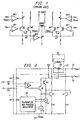
- FIG. 1 shows the simplified prior art circuit in Reference [1].
- Amplifier OP1 in conjunction with transistors M1 and M2, and resistor R2 provide an output impedance of R2/(1+N) due to the feedback.
- Amplifier OP3 forces input TXin and output TXout to be equal and hence sets the driver gain to one.
- Amplifiers OP1' and OP3', transistors M1' and M2', and resistor R2' perform the same for the negative input. This ensures that the impedance matches that of the output line. Amplifier OP2 stops DC loss in the outputs, as the output common mode is forced to the same voltage.
- the major draw backs of this method is the limited output swing, the extra trimming needed for the correct synthesized impedance, and the extra low frequency tuning loop needed to avoid DC loss in the termination.
- a line driver circuit comprises: a differential circuit having first and second input nodes, first and second output nodes, and a supply voltage node; a transformer having a first coil coupled between the first and second output nodes; and a center tap of the first coil coupled to the supply voltage node.
- a preferred embodiment power efficient line driver with terminating impedance synthesis circuit is shown in Figure 2.
- the device of Figure 2 includes amplifier 20; transistors Q1, Q1', Q2, and Q2'; resistors R1, R1', R3, R3', R4, R4', R5, and R5'; current sources G1 and G1'; transformer 22; resistance RL; temperature/process adjustment device 24; supply voltage VDD; and common node 26.
- Transformer 22 is a 1:1 transformer.
- Resistance RL represents the line impedance of a transmission line such as a coaxial cable or twisted pair.
- the preferred embodiment line driver of Figure 2 achieves two times the voltage swing as compared to prior art systems which use the same transformer turns ratio.
- R5) If R1 is >> Re, then the above equation simplifies to: Rout 2*R1*(R3+(R4
- This solution produces a peak-to-peak signal swing equal to 4 times the supply voltage which provides an excellent solution for low voltage systems.
- the need for series terminating resistors is eliminated with this circuit. This eliminates power dissipation across those resistors thereby increasing the efficiency of the circuit.
- This solution also eliminates the need for external resistors or capacitors thereby reducing the external component count.
Landscapes
- Engineering & Computer Science (AREA)
- Power Engineering (AREA)
- Computer Networks & Wireless Communication (AREA)
- Signal Processing (AREA)
- Logic Circuits (AREA)
- Amplifiers (AREA)
- Cable Transmission Systems, Equalization Of Radio And Reduction Of Echo (AREA)
- Dc Digital Transmission (AREA)
Abstract
Description
- This invention generally relates to electronic systems, and more particularly it relates to power efficient line drivers.
- Analog front-ends for Digital Subscriber Line (DSL) and Local Area Network (LAN) increasingly require to operate at lower supply voltages while larger output line driver voltages are required for operation on longer loops as well as enabling multilevel modulation for higher bit rate transmissions. At the lower supply voltage levels power efficiency is even more critical and hence 6dB signal loss in terminating/matching resistors is significant. One solution to raise the output signal level would be to use a higher turn ratio transformer. The problem with this apart from the cost is that the receiver input noise specification would need to be reduced by the same ratio. Prior art References [1] B. Nauta and M. Dijkstra, "Analog Video Line Driver with Adaptive Impedance Matching" ISSCC Digest of Technical Papers, pp. 318-319, Feb. 1998 and [2] Rajeevan Mahadevan and David Johns, "A Differential 160MHz Self-Terminating Adaptive CMOS Line Driver" ISSCC Digest of Technical Papers, pp. 436-437, Feb. 2000 discuss single-ended and differential methods of synthesizing the terminating impedances respectively. Figure 1 shows the simplified prior art circuit in Reference [1]. Amplifier OP1 in conjunction with transistors M1 and M2, and resistor R2 provide an output impedance of R2/(1+N) due to the feedback. Amplifier OP3 forces input TXin and output TXout to be equal and hence sets the driver gain to one. Amplifiers OP1' and OP3', transistors M1' and M2', and resistor R2' perform the same for the negative input. This ensures that the impedance matches that of the output line. Amplifier OP2 stops DC loss in the outputs, as the output common mode is forced to the same voltage. The circuit can be used as an impedance synthesizer by disabling the loop which forces TXin=TXout. This allows gain to be achieved in the driver stage.
- The major draw backs of this method is the limited output swing, the extra trimming needed for the correct synthesized impedance, and the extra low frequency tuning loop needed to avoid DC loss in the termination.
- Generally, and in one form of the invention, a line driver circuit is provided that comprises: a differential circuit having first and second input nodes, first and second output nodes, and a supply voltage node; a transformer having a first coil coupled between the first and second output nodes; and a center tap of the first coil coupled to the supply voltage node.
- The present invention will now be further described by way of example, with reference to the preferred and illustrative embodiments shown in the figures of the accompanying drawings in which:
- FIG. 1 is a circuit diagram of a prior art line driver;
- FIG. 2 is a circuit diagram of a preferred embodiment power efficient line driver with active termination synthesizer.
-
- A preferred embodiment power efficient line driver with terminating impedance synthesis circuit is shown in Figure 2. The device of Figure 2 includes amplifier 20; transistors Q1, Q1', Q2, and Q2'; resistors R1, R1', R3, R3', R4, R4', R5, and R5'; current sources G1 and G1';
transformer 22; resistance RL; temperature/process adjustment device 24; supply voltage VDD; andcommon node 26. Transformer 22 is a 1:1 transformer. Resistance RL represents the line impedance of a transmission line such as a coaxial cable or twisted pair. The preferred embodiment line driver of Figure 2 achieves two times the voltage swing as compared to prior art systems which use the same transformer turns ratio. With a single ended voltage supply of 5 volts, a theoretical differential peak-to-peak swing of 20 volts is possible with this circuit. This is achieved by thetransformer center tap 50 biased to the supply voltage VDD which allows the driver output atnodes - The synthesized impedance is calculated as follows:
- Several advantages are provided by the preferred embodiment circuit of Figure 2. This solution produces a peak-to-peak signal swing equal to 4 times the supply voltage which provides an excellent solution for low voltage systems. The need for series terminating resistors is eliminated with this circuit. This eliminates power dissipation across those resistors thereby increasing the efficiency of the circuit. This solution also eliminates the need for external resistors or capacitors thereby reducing the external component count.
- While this invention has been described with reference to an illustrative embodiment, this description is not intended to be construed in a limiting sense. Various modifications and combinations of the illustrative embodiment, as well as other embodiments of the invention, will be apparent to persons skilled in the art upon reference to the description. It is therefore intended that the appended claims encompass any such modifications or embodiments.
Claims (17)
- A circuit comprising:a differential circuit having first and second input nodes, first and second output nodes, and a supply voltage node;a transformer having a first coil coupled between the first and second output nodes; anda center tap of the first coil coupled to the supply voltage node.
- The circuit of claim 1 wherein the differential circuit comprises:an amplifier coupled between the first and second input nodes and the first and second output nodes;a first resistance coupled between the first input node and the first output node;a second resistance coupled between the second input node and the second output node;a third resistance coupled between the first output node and a common node; anda fourth resistance coupled between the second output node and the common node.
- The circuit of claim 2 wherein the first resistance comprises:a first resistor coupled between the first input node and a first input node of the amplifier; anda second resistor coupled between the first input node of the amplifier and the first output node.
- The circuit of claim 3 wherein the second resistance comprises:a third resistor coupled between the second input node and a second input node of the amplifier; anda fourth resistor coupled between the second input node of the amplifier and the second output node.
- The circuit of claim 4 further comprising:a fifth resistor coupled between the first input node of the amplifier and the common node; anda sixth resistor coupled between the second input node of the amplifier and the common node.
- The circuit of claim 2 wherein the third resistance comprises:a first resistor coupled to the common node; anda first transistor coupled between the first resistor and the first output node.
- The circuit of claim 6 wherein the fourth resistance comprises:a second resistor coupled to the common node; anda second transistor coupled between the second resistor and the second output node.
- The circuit of claim 7 further comprising:a third transistor coupled between a control node of the first transistor and the center tap, a control node of the third transistor is coupled to a first output of the amplifier; anda fourth transistor coupled between a control node of the second transistor and the center tap, a control node of the fourth transistor is coupled to a second output of the amplifier.
- The circuit of claim 8 further comprising:a first current source coupled between the third transistor and the common node; anda second current source coupled between the fourth transistor and the common node.
- The circuit of claim 1 wherein a second coil of the transformer is coupled to a transmission line.
- A circuit comprising:an amplifier;a first transistor having a control node coupled to a first output node of the amplifier;a second transistor having a control node coupled to a second output node of the amplifier;a third transistor having a control node coupled to a first end of the first transistor;a fourth transistor having a control node coupled to a first end of the second transistor; anda first coil of a transformer having a first end coupled to a first end of the third transistor, a second end coupled to a first end of the fourth transistor, and a center tap coupled to a first end of the first transistor and to a first end of the second transistor.
- The circuit of claim 11 further comprising:a first resistor coupled between a second end of the third transistor and a common node; anda second resistor coupled between a second end of the fourth transistor and the common node.
- The circuit of claim 11 further comprising:a first resistor coupled between a first input node of the amplifier and the first end of the first coil; anda second resistor coupled between a second input node of the amplifier and the second end of the first coil.
- The circuit of claim 13 further comprising:a third resistor coupled between the first input node of the amplifier and a positive input node; anda fourth resistor coupled between the second input node of the amplifier and a negative input node.
- The circuit of claim 14 further comprising:a fifth resistor coupled between the first input node of the amplifier and a common node; anda sixth resistor coupled between the second input node of the amplifier and a common node.
- The circuit of claim 11 further comprising:a first current source coupled to a second end of the first transistor; anda second current source coupled to a second end of the second transistor.
- The circuit of claim 11 further comprising a second coil of the transformer coupled to a transmission line.
Applications Claiming Priority (2)
| Application Number | Priority Date | Filing Date | Title |
|---|---|---|---|
| US22928500P | 2000-08-31 | 2000-08-31 | |
| US229285P | 2000-08-31 |
Publications (2)
| Publication Number | Publication Date |
|---|---|
| EP1185045A2 true EP1185045A2 (en) | 2002-03-06 |
| EP1185045A3 EP1185045A3 (en) | 2005-09-14 |
Family
ID=22860552
Family Applications (1)
| Application Number | Title | Priority Date | Filing Date |
|---|---|---|---|
| EP01000412A Withdrawn EP1185045A3 (en) | 2000-08-31 | 2001-08-30 | Differential line driver |
Country Status (4)
| Country | Link |
|---|---|
| US (1) | US6538500B2 (en) |
| EP (1) | EP1185045A3 (en) |
| JP (1) | JP2002176457A (en) |
| KR (1) | KR20020018171A (en) |
Families Citing this family (4)
| Publication number | Priority date | Publication date | Assignee | Title |
|---|---|---|---|---|
| US7573839B2 (en) * | 2004-07-07 | 2009-08-11 | Broadcom Corporation | Line driver for an adaptive hybrid circuit |
| WO2012103826A2 (en) * | 2012-03-15 | 2012-08-09 | 华为技术有限公司 | Line driving method and device |
| CN104617900B (en) * | 2015-01-19 | 2017-12-08 | 信阳农林学院 | A kind of network signal transmits amplifying circuit |
| JP2022067573A (en) * | 2020-10-20 | 2022-05-06 | 株式会社村田製作所 | Power amplifier circuit |
Family Cites Families (3)
| Publication number | Priority date | Publication date | Assignee | Title |
|---|---|---|---|---|
| US5912924A (en) * | 1996-08-15 | 1999-06-15 | Seeq Technology, Inc. | Bidirectional channels using common pins for transmit and receive paths |
| US6177789B1 (en) * | 2000-01-31 | 2001-01-23 | National Semiconductor Corporation | Line driver for producing operating condition invariant signal levels |
| US6307765B1 (en) * | 2000-06-22 | 2001-10-23 | Linfinity Microelectronics | Method and apparatus for controlling minimum brightness of a fluorescent lamp |
-
2001
- 2001-08-24 US US09/938,776 patent/US6538500B2/en not_active Expired - Lifetime
- 2001-08-30 JP JP2001261594A patent/JP2002176457A/en active Pending
- 2001-08-30 EP EP01000412A patent/EP1185045A3/en not_active Withdrawn
- 2001-08-31 KR KR1020010053161A patent/KR20020018171A/en not_active Withdrawn
Non-Patent Citations (2)
| Title |
|---|
| EVERITT J ET AL: "CMOS TRANSCEIVER FOR 10-MB/S AND 100-MB/S ETHERNET" IEEE JOURNAL OF SOLID-STATE CIRCUITS, IEEE INC. NEW YORK, US, vol. 33, no. 12, December 1998 (1998-12), pages 2169-2177, XP000880522 ISSN: 0018-9200 * |
| HAIDEH KHORRAMABADI: "A CMOS LINE DRIVER WITH 80-DB LINEARITY FOR ISDN APPLICATIONS" IEICE TRANSACTIONS ON ELECTRONICS, INSTITUTE OF ELECTRONICS INFORMATION AND COMM. ENG. TOKYO, JP, vol. E75 - C, no. 4, 1 April 1992 (1992-04-01), pages 437-442, XP000301673 ISSN: 0916-8524 * |
Also Published As
| Publication number | Publication date |
|---|---|
| KR20020018171A (en) | 2002-03-07 |
| JP2002176457A (en) | 2002-06-21 |
| US6538500B2 (en) | 2003-03-25 |
| EP1185045A3 (en) | 2005-09-14 |
| US20020024381A1 (en) | 2002-02-28 |
Similar Documents
| Publication | Publication Date | Title |
|---|---|---|
| US7456650B2 (en) | Memory system with stable termination of a pair of differential signals transmitted via a pair of transmission lines | |
| US7501853B2 (en) | Data processing circuit | |
| KR101965788B1 (en) | Single-ended configurable multi-mode driver | |
| US20070002954A1 (en) | Hybrid voltage/current-mode transmission line driver | |
| KR100310550B1 (en) | Line driver with adaptive output impedance | |
| US5977819A (en) | CMOS gigabit serial link differential transmitter and receiver | |
| US20040096005A1 (en) | Gigabit ethernet line driver and hybrid architecture | |
| EP1168740A2 (en) | Line driver with adaptive impedance | |
| US7982538B2 (en) | Differential output circuit and communication device | |
| EP2412136A2 (en) | Voltage mode transmitter equalizer | |
| JP2004015822A (en) | Variable equalizing amplifier | |
| US20020113626A1 (en) | Differential line driver having adjustable common mode operation | |
| JPH04290368A (en) | Power feeding transfer system | |
| JP2002344300A (en) | Impedance adjustment circuit | |
| JPH07202675A (en) | Transceiver circuit | |
| US6316927B1 (en) | Voltage output driver and filter | |
| US6166570A (en) | Output buffer circuit with switchable common mode output level | |
| US6307402B1 (en) | Output buffer for driving a symmetrical transmission line | |
| US7483688B2 (en) | Network device with hybrid-mode transmitter | |
| EP0606888B1 (en) | Communication line driver, LSI for interface including such a circuit and communication terminal apparatus | |
| US6538500B2 (en) | Power efficient line driver with 4X supply voltage swing and active termination | |
| US5510745A (en) | High-speed electronic circuit having a cascode configuration | |
| US7450649B2 (en) | Current mode digital data transmitter | |
| US5805031A (en) | Transistor ratio controlled CMOS transmission line equalizer | |
| US20050030820A1 (en) | Simultaneous bi-directional transceiver |
Legal Events
| Date | Code | Title | Description |
|---|---|---|---|
| PUAI | Public reference made under article 153(3) epc to a published international application that has entered the european phase |
Free format text: ORIGINAL CODE: 0009012 |
|
| AK | Designated contracting states |
Kind code of ref document: A2 Designated state(s): AT BE CH CY DE DK ES FI FR GB GR IE IT LI LU MC NL PT SE TR |
|
| AX | Request for extension of the european patent |
Free format text: AL;LT;LV;MK;RO;SI |
|
| PUAL | Search report despatched |
Free format text: ORIGINAL CODE: 0009013 |
|
| AK | Designated contracting states |
Kind code of ref document: A3 Designated state(s): AT BE CH CY DE DK ES FI FR GB GR IE IT LI LU MC NL PT SE TR |
|
| AX | Request for extension of the european patent |
Extension state: AL LT LV MK RO SI |
|
| 17P | Request for examination filed |
Effective date: 20060314 |
|
| AKX | Designation fees paid |
Designated state(s): DE FR GB |
|
| 17Q | First examination report despatched |
Effective date: 20060822 |
|
| STAA | Information on the status of an ep patent application or granted ep patent |
Free format text: STATUS: THE APPLICATION IS DEEMED TO BE WITHDRAWN |
|
| 18D | Application deemed to be withdrawn |
Effective date: 20070103 |