EP1184969A1 - Frequency-generator circuit - Google Patents
Frequency-generator circuit Download PDFInfo
- Publication number
- EP1184969A1 EP1184969A1 EP00117613A EP00117613A EP1184969A1 EP 1184969 A1 EP1184969 A1 EP 1184969A1 EP 00117613 A EP00117613 A EP 00117613A EP 00117613 A EP00117613 A EP 00117613A EP 1184969 A1 EP1184969 A1 EP 1184969A1
- Authority
- EP
- European Patent Office
- Prior art keywords
- frequency
- circuit
- oscillator
- resonator
- bias
- Prior art date
- Legal status (The legal status is an assumption and is not a legal conclusion. Google has not performed a legal analysis and makes no representation as to the accuracy of the status listed.)
- Granted
Links
- 238000010168 coupling process Methods 0.000 claims description 12
- 238000005859 coupling reaction Methods 0.000 claims description 12
- 230000008878 coupling Effects 0.000 claims description 11
- 230000000694 effects Effects 0.000 claims description 2
- 238000005086 pumping Methods 0.000 description 2
- 230000009471 action Effects 0.000 description 1
- 230000002238 attenuated effect Effects 0.000 description 1
- 230000008901 benefit Effects 0.000 description 1
- 239000000919 ceramic Substances 0.000 description 1
- 238000013016 damping Methods 0.000 description 1
- 230000001419 dependent effect Effects 0.000 description 1
- 238000010586 diagram Methods 0.000 description 1
- 238000001914 filtration Methods 0.000 description 1
- PCHJSUWPFVWCPO-UHFFFAOYSA-N gold Chemical compound [Au] PCHJSUWPFVWCPO-UHFFFAOYSA-N 0.000 description 1
- 239000010931 gold Substances 0.000 description 1
- 229910052737 gold Inorganic materials 0.000 description 1
- 230000007246 mechanism Effects 0.000 description 1
- 238000000034 method Methods 0.000 description 1
- 230000010355 oscillation Effects 0.000 description 1
- 230000003071 parasitic effect Effects 0.000 description 1
- 238000004088 simulation Methods 0.000 description 1
- 239000000758 substrate Substances 0.000 description 1
- 239000010409 thin film Substances 0.000 description 1
- 238000009966 trimming Methods 0.000 description 1
- 238000011144 upstream manufacturing Methods 0.000 description 1
Images


Classifications
-
- H—ELECTRICITY
- H03—ELECTRONIC CIRCUITRY
- H03B—GENERATION OF OSCILLATIONS, DIRECTLY OR BY FREQUENCY-CHANGING, BY CIRCUITS EMPLOYING ACTIVE ELEMENTS WHICH OPERATE IN A NON-SWITCHING MANNER; GENERATION OF NOISE BY SUCH CIRCUITS
- H03B5/00—Generation of oscillations using amplifier with regenerative feedback from output to input
- H03B5/18—Generation of oscillations using amplifier with regenerative feedback from output to input with frequency-determining element comprising distributed inductance and capacitance
- H03B5/1864—Generation of oscillations using amplifier with regenerative feedback from output to input with frequency-determining element comprising distributed inductance and capacitance the frequency-determining element being a dielectric resonator
- H03B5/187—Generation of oscillations using amplifier with regenerative feedback from output to input with frequency-determining element comprising distributed inductance and capacitance the frequency-determining element being a dielectric resonator the active element in the amplifier being a semiconductor device
- H03B5/1876—Generation of oscillations using amplifier with regenerative feedback from output to input with frequency-determining element comprising distributed inductance and capacitance the frequency-determining element being a dielectric resonator the active element in the amplifier being a semiconductor device the semiconductor device being a field-effect device
-
- H—ELECTRICITY
- H03—ELECTRONIC CIRCUITRY
- H03B—GENERATION OF OSCILLATIONS, DIRECTLY OR BY FREQUENCY-CHANGING, BY CIRCUITS EMPLOYING ACTIVE ELEMENTS WHICH OPERATE IN A NON-SWITCHING MANNER; GENERATION OF NOISE BY SUCH CIRCUITS
- H03B19/00—Generation of oscillations by non-regenerative frequency multiplication or division of a signal from a separate source
- H03B19/05—Generation of oscillations by non-regenerative frequency multiplication or division of a signal from a separate source using non-linear capacitance, e.g. varactor diodes
-
- H—ELECTRICITY
- H03—ELECTRONIC CIRCUITRY
- H03B—GENERATION OF OSCILLATIONS, DIRECTLY OR BY FREQUENCY-CHANGING, BY CIRCUITS EMPLOYING ACTIVE ELEMENTS WHICH OPERATE IN A NON-SWITCHING MANNER; GENERATION OF NOISE BY SUCH CIRCUITS
- H03B25/00—Simultaneous generation by a free-running oscillator of oscillations having different frequencies
-
- H—ELECTRICITY
- H03—ELECTRONIC CIRCUITRY
- H03B—GENERATION OF OSCILLATIONS, DIRECTLY OR BY FREQUENCY-CHANGING, BY CIRCUITS EMPLOYING ACTIVE ELEMENTS WHICH OPERATE IN A NON-SWITCHING MANNER; GENERATION OF NOISE BY SUCH CIRCUITS
- H03B5/00—Generation of oscillations using amplifier with regenerative feedback from output to input
- H03B5/08—Generation of oscillations using amplifier with regenerative feedback from output to input with frequency-determining element comprising lumped inductance and capacitance
- H03B5/12—Generation of oscillations using amplifier with regenerative feedback from output to input with frequency-determining element comprising lumped inductance and capacitance active element in amplifier being semiconductor device
- H03B5/1203—Generation of oscillations using amplifier with regenerative feedback from output to input with frequency-determining element comprising lumped inductance and capacitance active element in amplifier being semiconductor device the amplifier being a single transistor
-
- H—ELECTRICITY
- H03—ELECTRONIC CIRCUITRY
- H03B—GENERATION OF OSCILLATIONS, DIRECTLY OR BY FREQUENCY-CHANGING, BY CIRCUITS EMPLOYING ACTIVE ELEMENTS WHICH OPERATE IN A NON-SWITCHING MANNER; GENERATION OF NOISE BY SUCH CIRCUITS
- H03B5/00—Generation of oscillations using amplifier with regenerative feedback from output to input
- H03B5/08—Generation of oscillations using amplifier with regenerative feedback from output to input with frequency-determining element comprising lumped inductance and capacitance
- H03B5/12—Generation of oscillations using amplifier with regenerative feedback from output to input with frequency-determining element comprising lumped inductance and capacitance active element in amplifier being semiconductor device
- H03B5/1228—Generation of oscillations using amplifier with regenerative feedback from output to input with frequency-determining element comprising lumped inductance and capacitance active element in amplifier being semiconductor device the amplifier comprising one or more field effect transistors
-
- H—ELECTRICITY
- H03—ELECTRONIC CIRCUITRY
- H03B—GENERATION OF OSCILLATIONS, DIRECTLY OR BY FREQUENCY-CHANGING, BY CIRCUITS EMPLOYING ACTIVE ELEMENTS WHICH OPERATE IN A NON-SWITCHING MANNER; GENERATION OF NOISE BY SUCH CIRCUITS
- H03B5/00—Generation of oscillations using amplifier with regenerative feedback from output to input
- H03B5/08—Generation of oscillations using amplifier with regenerative feedback from output to input with frequency-determining element comprising lumped inductance and capacitance
- H03B5/12—Generation of oscillations using amplifier with regenerative feedback from output to input with frequency-determining element comprising lumped inductance and capacitance active element in amplifier being semiconductor device
- H03B5/1237—Generation of oscillations using amplifier with regenerative feedback from output to input with frequency-determining element comprising lumped inductance and capacitance active element in amplifier being semiconductor device comprising means for varying the frequency of the generator
- H03B5/124—Generation of oscillations using amplifier with regenerative feedback from output to input with frequency-determining element comprising lumped inductance and capacitance active element in amplifier being semiconductor device comprising means for varying the frequency of the generator the means comprising a voltage dependent capacitance
- H03B5/1243—Generation of oscillations using amplifier with regenerative feedback from output to input with frequency-determining element comprising lumped inductance and capacitance active element in amplifier being semiconductor device comprising means for varying the frequency of the generator the means comprising a voltage dependent capacitance the means comprising voltage variable capacitance diodes
Definitions
- the invention relates to a frequency-generator circuit containing a parametric frequency-divider.
- Oscillators for use in phase-locked loops often require a frequency-divider section to reduce the input frequency to a value which can be handled by the phase detector.
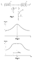
- a frequency-divider which operates on the parametric principle is disclosed in German patent DE 195 29 529 issued on 31 October 1996 to Robert Bosch GmbH and is shown in Figure 1.
- the central element is a varactor diode 10 which acts as a non-linear reactance.
- an input filter 11 which is a high-pass filter tuned to the frequency of the input signal E and functions also as an impedance transformer matching the impedance of the line at the input of the circuit to the lower input impedance of the diode 10.
- a bias network for the diode 10 comprises an L-C circuit 13, via which a bias voltage U v is fed to the diode.
- a resistance R provides damping so that energy is not absorbed by the L-C network and no undesired oscillations are generated therein.
- a diode is required having a high gamma ( ⁇ ) over at least a part of its capacitance-voltage characteristic.
- Figure 2 shows a typical gamma characteristic with variation in gamma plotted against applied voltage U. In this particular case the diode is biased so that it is operating in the region defined by the value U v , i.e at the point at which gamma is maximum.
- a dielectric resonator 20 consisting of a ceramic disk, has on one side a microstrip 21, which is coupled at one end to an oscillator device 22, e.g. as illustrated a FET or a monolithic integrated oscillator circuit, and at the other end to ground via a matching impedance 23, while on the other side of the resonator 20 a second microstrip 24 is terminated at one end to ground by way of a varactor diode 25 and at the other end is unterminated, but is trimmable due to the presence of the trimming arrangement 27.
- an oscillator device 22 e.g. as illustrated a FET or a monolithic integrated oscillator circuit
- a second microstrip 24 is terminated at one end to ground by way of a varactor diode 25 and at the other end is unterminated, but is trimmable due to the presence of the trimming arrangement 27.
- This may comprise a series of narrow wire-bondable line-sections, as shown, or a continuous section consisting of easily laser-trimmable thin-film sputtergold, in contrast to the much thicker galvanically produced gold of the rest of the line 24.
- a biasing voltage U DC is applied to the varactor by way of an L-C biasing network 26.
- the oscillator transistor 22 is operated in negative-resistance mode by virtue of the transistor having a positive reflection factor
- the varactor 25 functions in this circuit not only as a parametric frequency-divider, which requires that it be biased so as to operate at its maximum, or a suitably high, gamma value as in the case of Figure 1, but also as a frequency-adjusting element for the oscillator arrangement 20, 21, 22.
- the varactor should ideally have a substantially flat gamma-characteristic over its operating-voltage range in contrast to the noticeably peaked characteristic evident from Figure 2.
- Such a preferred characteristic is shown in Figure 4, in which can also be seen the range of bias-voltage variation, U DC , which can be employed to vary the capacitance of the varactor and hence trim the operating frequency of the oscillator circuit.
- the oscillator drives ("pumps") the diode 25 at a frequency F and this, due to the non-linear capacitance-voltage characteristic of the diode, gives rise to a negative resistance in the diode at the subharmonic divider frequency.
- this negative resistance is greater than the positive loss-resistance of the diode, the diode oscillates at that subharmonic (division factor 2, 3, 4...), provided the microstrip 24 is suitably dimensioned.
- L min has to be determined by extensive simulation and in this case is made to satisfy a tradeoff between the obtaining of linear tuning at pump frequency, F, and the obtaining of a negative resistance at the divided frequency.
- the divided frequency e.g. F/2
- F linear tuning at pump frequency
- F/2 the divided frequency
- An alternative measure is to provide a coupling element 29 adjacent to the microstrip 24, one end of the coupling element being grounded via a matching impedance 30, the other acting as the F/2 output.
- the parametric operation of the varactor relies on the provision of a sufficiently high pump-signal amplitude to drive the varactor.
- the oscillator element e.g. FET
- + 10dB.
- the oscillator element is operated as a high negative resistance, e.g.
- + 10dB.
- the varactor-diode resonance circuit comprising items 24, 25 and 27 is very well isolated from the rest of the circuit.
- the dielectric resonator is replaced by a ring resonator (see Figure 5).
- the only essential difference is the mechanism by which resonance is determined: in the case of the dielectric resonator it is the diameter and height above the circuit board of the dielectric disk which sets the resonance frequency, whereas in the ring-resonator case it is the diameter of the conductive ring 40 which is the governing factor.
- the frequency-divided signal (at frequency F/2) couples from the varactor network via its coupling line 41 and the resonator 40 to the coupling line 42 of the active oscillator device 22.
- This oscillator device amplifies the frequency-divided signal as well as the pump frequency and both signals are available at the output 28.
- the coupling-out of the divider signal can take place as illustrated in Figure 6, in which a coupling line 43, similar to the coupling line 29 of Figure 3, is disposed adjacent, but in loose-coupling relationship, to line 42, or as illustrated in Figure 7, in which the coupling line 43 couples to the output 28 of the FET (or similar) stage 22 (in this case coupler 43 advantageously couples out an amplified version of the divided frequency), or as shown in Figure 8, in which the signal at the output 28 is taken to a diplexer 44, which separates out the signals.
- This latter arrangement results in fewer losses than the Figure 6 or Figure 7 arrangements, however all three arrangements have the advantage that the available extracted power is much higher than with the Figure 3 or Figure 5 schemes.
- a frequency-generator with parametric frequency-divider and frequency-adjustment facility which is based on the use of only one device to perform both frequency-division and frequency-adjustment. Because of this and the lack of a need to include both input and output filters, the generator is more economical to produce than prior-art generators. It is also capable of providing frequency-division at very high frequencies (>20GHz) so that it can be implemented in PLL-circuits operating at > 30GHz.
Landscapes
- Physics & Mathematics (AREA)
- Nonlinear Science (AREA)
- Inductance-Capacitance Distribution Constants And Capacitance-Resistance Oscillators (AREA)
- Control Of Eletrric Generators (AREA)
- General Induction Heating (AREA)
- Oscillators With Electromechanical Resonators (AREA)
Abstract
Description
- The invention relates to a frequency-generator circuit containing a parametric frequency-divider.
- Oscillators for use in phase-locked loops (PLLs) often require a frequency-divider section to reduce the input frequency to a value which can be handled by the phase detector. An example of a frequency-divider which operates on the parametric principle is disclosed in German patent DE 195 29 529 issued on 31 October 1996 to Robert Bosch GmbH and is shown in Figure 1. In Figure 1 the central element is a varactor diode 10 which acts as a non-linear reactance. Upstream of the diode is an input filter 11, which is a high-pass filter tuned to the frequency of the input signal E and functions also as an impedance transformer matching the impedance of the line at the input of the circuit to the lower input impedance of the diode 10. Downstream of the diode is an output filter 12, which is a low-pass filter tuned to the divided-down frequency of the output signal A and also functions as an impedance transformer in the reverse sense to that of the input filter 11. A bias network for the diode 10 comprises an L-C circuit 13, via which a bias voltage Uv is fed to the diode. A resistance R provides damping so that energy is not absorbed by the L-C network and no undesired oscillations are generated therein.
- The varactor 10 possesses a capacitance-voltage characteristic given by the expression:
- While this known circuit provides frequency-division at very low phase-noise, for example, it involves quite a lot of outlay considering it must also be used in conjunction with an oscillator having some form of additional frequency-adjusting facility.
- In accordance with the present invention there is provided a frequency-generator circuit as recited in Claim 1. Advantageous realisations of the circuit are set forth in the subclaims.
- Embodiments of the invention will now be described, by way of example only, with reference to the drawings, of which:
- Figure 1 is a circuit diagram of a prior-art frequency-divider arrangement;
- Figure 2 is a graph showing the variation of gamma against voltage for a typical varactor diode;
- Figure 3 illustrates a first embodiment of an oscillator circuit in accordance with the invention;
- Figure 4 is a graph of gamma versus bias-voltage for a varactor diode suitable for use in the present invention, and
- Figures 5, 6, 7 and 8 illustrate first, second, third and fourth realisations of a second embodiment of an oscillator circuit in accordance with the invention.
-
- Referring to Figure 3, a first embodiment of the invention is illustrated in which a dielectric resonator 20, consisting of a ceramic disk, has on one side a microstrip 21, which is coupled at one end to an oscillator device 22, e.g. as illustrated a FET or a monolithic integrated oscillator circuit, and at the other end to ground via a matching impedance 23, while on the other side of the resonator 20 a second microstrip 24 is terminated at one end to ground by way of a varactor diode 25 and at the other end is unterminated, but is trimmable due to the presence of the trimming arrangement 27. This may comprise a series of narrow wire-bondable line-sections, as shown, or a continuous section consisting of easily laser-trimmable thin-film sputtergold, in contrast to the much thicker galvanically produced gold of the rest of the line 24. A biasing voltage UDC is applied to the varactor by way of an L-C biasing network 26. The oscillator transistor 22 is operated in negative-resistance mode by virtue of the transistor having a positive reflection factor |S11| > 1.
- The varactor 25 functions in this circuit not only as a parametric frequency-divider, which requires that it be biased so as to operate at its maximum, or a suitably high, gamma value as in the case of Figure 1, but also as a frequency-adjusting element for the oscillator arrangement 20, 21, 22. To this end the varactor should ideally have a substantially flat gamma-characteristic over its operating-voltage range in contrast to the noticeably peaked characteristic evident from Figure 2. Such a preferred characteristic is shown in Figure 4, in which can also be seen the range of bias-voltage variation, UDC, which can be employed to vary the capacitance of the varactor and hence trim the operating frequency of the oscillator circuit. A wider range of bias-voltage variation could be tolerated, but this would then entail a lower mean value of gamma, which in turn would reduce pumping efficiency. Employing a diode having a constant gamma of > 2 will provide a substantially linear frequency-adjusting effect and also result in low pumping power-drain on the oscillator arrangement.
- The oscillator drives ("pumps") the diode 25 at a frequency F and this, due to the non-linear capacitance-voltage characteristic of the diode, gives rise to a negative resistance in the diode at the subharmonic divider frequency. When this negative resistance is greater than the positive loss-resistance of the diode, the diode oscillates at that subharmonic (division factor 2, 3, 4...), provided the microstrip 24 is suitably dimensioned. The length of the strip 24 determines both the slope of the varactor tuning characteristic and the division ratio and in respect of the latter the following relationship applies:
- The parametric operation of the varactor relies on the provision of a sufficiently high pump-signal amplitude to drive the varactor. To achieve this, in a preferred form of the invention the oscillator element (e.g. FET) is operated as a high negative resistance, e.g. |S11| = + 10dB. This in turn allows a loose coupling of the resonator 20 to the strips 21 and 24, which increases the loaded resonator Q-factor, with the result that the higher energy stored in the resonator gives rise to a larger HF voltage amplitude at the varactor. In addition, because of the relatively weak coupling of the oscillator and resonator with the divider output 29, the varactor-diode resonance circuit comprising items 24, 25 and 27 is very well isolated from the rest of the circuit.
- In a second embodiment of the invention, the dielectric resonator is replaced by a ring resonator (see Figure 5). In the arrangement illustrated in Figure 5 the only essential difference is the mechanism by which resonance is determined: in the case of the dielectric resonator it is the diameter and height above the circuit board of the dielectric disk which sets the resonance frequency, whereas in the ring-resonator case it is the diameter of the conductive ring 40 which is the governing factor.
- Three alternative realisations of the second embodiment are shown in Figures 6, 7 and 8 (in Figures 7 and 8 the resonator and varactor-related components are omitted for the sake of convenience). In all three cases the resonator circumference is designed to be, in wavelengths, an integer multiple m of the division factor n, i.e. for n=2 the diameter is 2m. (In the Figure 5 case it was assumed that the circumference was of length, λ, 2λ, 3λ, etc). The situation now is that, since the ring-resonator is in resonance not only at frequency F, but also at frequency F/2, the frequency-divided signal (at frequency F/2) couples from the varactor network via its coupling line 41 and the resonator 40 to the coupling line 42 of the active oscillator device 22. This oscillator device amplifies the frequency-divided signal as well as the pump frequency and both signals are available at the output 28. The coupling-out of the divider signal can take place as illustrated in Figure 6, in which a coupling line 43, similar to the coupling line 29 of Figure 3, is disposed adjacent, but in loose-coupling relationship, to line 42, or as illustrated in Figure 7, in which the coupling line 43 couples to the output 28 of the FET (or similar) stage 22 (in this case coupler 43 advantageously couples out an amplified version of the divided frequency), or as shown in Figure 8, in which the signal at the output 28 is taken to a diplexer 44, which separates out the signals. This latter arrangement results in fewer losses than the Figure 6 or Figure 7 arrangements, however all three arrangements have the advantage that the available extracted power is much higher than with the Figure 3 or Figure 5 schemes.
- As well as the ability to provide integer frequency-division factors by the above-described techniques, it is also possible to generate odd non-integer division factors, e.g. 1.5, 3.5, etc). This can be achieved by mixing the integer-divided subharmonic divider frequency with the oscillator (pump) frequency.
- What has been described is a frequency-generator with parametric frequency-divider and frequency-adjustment facility which is based on the use of only one device to perform both frequency-division and frequency-adjustment. Because of this and the lack of a need to include both input and output filters, the generator is more economical to produce than prior-art generators. It is also capable of providing frequency-division at very high frequencies (>20GHz) so that it can be implemented in PLL-circuits operating at > 30GHz.
Claims (12)
- Frequency-generator circuit comprising an oscillator, a frequency-adjusting element associated with the oscillator and a parametric frequency-divider having a frequency-dividing element, wherein the oscillator is operational as a pump for the parametric frequency-divider and the frequency-adjusting element is operational also as said frequency-dividing element.
- Circuit as claimed in Claim 1, wherein the frequency-dividing element is operative as a negative-resistance element.
- Circuit as claimed in Claim 2, wherein the frequency-dividing element is a varactor diode.
- Circuit as claimed in Claim 3, comprising a bias-means (26) connected to the varactor diode for providing a bias-voltage therefore, the varactor diode having a gamma-value which is substantially constant over a predetermined range of said bias-voltage, the predetermined bias-voltage range corresponding to a predetermined range of frequency-adjustment.
- Circuit as claimed in Claim 4, wherein said gamma-value is ≥ approximately 2.
- Circuit as claimed in any one of the preceding claims, comprising a resonance means for establishing a frequency of operation of the oscillator.
- Circuit as claimed in Claim 6, wherein the resonance means is a dielectric resonator.
- Circuit as claimed in Claim 6, wherein the resonance means is a ring-resonator.
- Circuit as claimed in any one of Claims 6 to 8, wherein the oscillator provides a pump signal of an amplitude such that the frequency-dividing element becomes sufficiently negative-resistance to generate a parametric effect, while at the same time allowing a loose coupling between the resonator and the oscillator and between the resonator and the frequency-dividing element.
- Circuit as claimed in Claim 9, wherein the oscillator is a negative-resistance device.
- Circuit as claimed in Claim 10, wherein the negative-resistance device has a positive reflection factor of ≥ approximately 10dB.
- Frequency-generator circuit substantially as shown in, or as hereinbefore described with reference to, Figure 3 or Figure 5 in conjunction with Figure 4.
Priority Applications (6)
| Application Number | Priority Date | Filing Date | Title |
|---|---|---|---|
| EP00117613A EP1184969B1 (en) | 2000-08-16 | 2000-08-16 | Frequency-generator circuit |
| DE60007740T DE60007740T2 (en) | 2000-08-16 | 2000-08-16 | Frequency generator circuit |
| AT00117613T ATE257983T1 (en) | 2000-08-16 | 2000-08-16 | FREQUENCY GENERATOR CIRCUIT |
| US09/928,253 US6657508B2 (en) | 2000-08-16 | 2001-08-10 | Frequency-generator circuit |
| NO20013975A NO20013975L (en) | 2000-08-16 | 2001-08-15 | Frequency Generator Circuit |
| CN01125428A CN1340921A (en) | 2000-08-16 | 2001-08-15 | Frequency generator circuit |
Applications Claiming Priority (1)
| Application Number | Priority Date | Filing Date | Title |
|---|---|---|---|
| EP00117613A EP1184969B1 (en) | 2000-08-16 | 2000-08-16 | Frequency-generator circuit |
Publications (2)
| Publication Number | Publication Date |
|---|---|
| EP1184969A1 true EP1184969A1 (en) | 2002-03-06 |
| EP1184969B1 EP1184969B1 (en) | 2004-01-14 |
Family
ID=8169538
Family Applications (1)
| Application Number | Title | Priority Date | Filing Date |
|---|---|---|---|
| EP00117613A Expired - Lifetime EP1184969B1 (en) | 2000-08-16 | 2000-08-16 | Frequency-generator circuit |
Country Status (6)
| Country | Link |
|---|---|
| US (1) | US6657508B2 (en) |
| EP (1) | EP1184969B1 (en) |
| CN (1) | CN1340921A (en) |
| AT (1) | ATE257983T1 (en) |
| DE (1) | DE60007740T2 (en) |
| NO (1) | NO20013975L (en) |
Cited By (1)
| Publication number | Priority date | Publication date | Assignee | Title |
|---|---|---|---|---|
| RU2259005C1 (en) * | 2003-12-09 | 2005-08-20 | Московский государственный университет путей сообщения (МИИТ) | Reference wave shaper for coherent detection of relative 180° phase keyed signals |
Families Citing this family (2)
| Publication number | Priority date | Publication date | Assignee | Title |
|---|---|---|---|---|
| CN100420020C (en) * | 2003-11-26 | 2008-09-17 | 中颖电子(上海)有限公司 | Integrated circuit chip with built-in high precision frequency oscillator |
| DE102005016626B4 (en) * | 2005-04-12 | 2013-03-14 | Wipro Limited | Active parametric quadrature divider |
Citations (1)
| Publication number | Priority date | Publication date | Assignee | Title |
|---|---|---|---|---|
| US3662287A (en) * | 1971-02-24 | 1972-05-09 | Us Navy | Voltage controlled oscillator multiplier |
Family Cites Families (6)
| Publication number | Priority date | Publication date | Assignee | Title |
|---|---|---|---|---|
| FR2325240A1 (en) | 1974-11-08 | 1977-04-15 | Cgr Mev | Frequency divided X-band gunn diode oscillator for C-band - has varactor diode coupled to circuit tuned to two-thirds fundamental |
| US4380831A (en) | 1981-07-24 | 1983-04-19 | Rockwell International Corporation | Symmetric microwave mixer with improved isolation |
| CA1225126A (en) * | 1985-03-07 | 1987-08-04 | Robert G. Harrison | Microstrip - slotline frequency halver |
| EP0595377A1 (en) * | 1992-10-29 | 1994-05-04 | MIZAR S.p.A. | Frequency synthesis system for generating microwave oscillations |
| US5428838A (en) | 1993-07-13 | 1995-06-27 | Trw Inc. | Diode mixer implemented in a planar monolithic IC |
| US5819169A (en) | 1996-05-10 | 1998-10-06 | Northrop Grumman Corporation | High performance mixer structures for monolithic microwave integrated circuits |
-
2000
- 2000-08-16 DE DE60007740T patent/DE60007740T2/en not_active Expired - Lifetime
- 2000-08-16 AT AT00117613T patent/ATE257983T1/en not_active IP Right Cessation
- 2000-08-16 EP EP00117613A patent/EP1184969B1/en not_active Expired - Lifetime
-
2001
- 2001-08-10 US US09/928,253 patent/US6657508B2/en not_active Expired - Lifetime
- 2001-08-15 CN CN01125428A patent/CN1340921A/en active Pending
- 2001-08-15 NO NO20013975A patent/NO20013975L/en unknown
Patent Citations (1)
| Publication number | Priority date | Publication date | Assignee | Title |
|---|---|---|---|---|
| US3662287A (en) * | 1971-02-24 | 1972-05-09 | Us Navy | Voltage controlled oscillator multiplier |
Cited By (1)
| Publication number | Priority date | Publication date | Assignee | Title |
|---|---|---|---|---|
| RU2259005C1 (en) * | 2003-12-09 | 2005-08-20 | Московский государственный университет путей сообщения (МИИТ) | Reference wave shaper for coherent detection of relative 180° phase keyed signals |
Also Published As
| Publication number | Publication date |
|---|---|
| EP1184969B1 (en) | 2004-01-14 |
| CN1340921A (en) | 2002-03-20 |
| US20020036547A1 (en) | 2002-03-28 |
| DE60007740D1 (en) | 2004-02-19 |
| NO20013975L (en) | 2002-02-19 |
| DE60007740T2 (en) | 2004-07-01 |
| US6657508B2 (en) | 2003-12-02 |
| NO20013975D0 (en) | 2001-08-15 |
| ATE257983T1 (en) | 2004-01-15 |
Similar Documents
| Publication | Publication Date | Title |
|---|---|---|
| US5059927A (en) | Microwave oscillator with reduced phase noise | |
| EP1943659B1 (en) | Oscillating circuit with tunable filter for minimizing phase noise | |
| US9515605B1 (en) | Variable gain electro-mechanical oscillator and method for starting balanced oscillations | |
| US5231361A (en) | Voltage controlled push-push oscillator with parallel resonant tank circuits | |
| US10090805B2 (en) | Voltage-controlled oscillator and a method for tuning oscillations | |
| KR100457939B1 (en) | High frequency crystal oscillator | |
| US6472945B1 (en) | Operational amplifier oscillator | |
| EP1184969B1 (en) | Frequency-generator circuit | |
| US10958213B2 (en) | Pullable clock oscillator | |
| US7199674B2 (en) | Low phase noise, wide tune range saw oscillators and methods of operating the same | |
| US4630004A (en) | Dielectric resonator stabilized microstrip oscillator | |
| Driscoll | Low noise, microwave signal generation using bulk and surface acoustic wave resonators | |
| US6967540B2 (en) | Synthesizers incorporating parascan TM varactors | |
| Hitch et al. | Phase locked DRO/CRO for space use | |
| EP1188227B1 (en) | Voltage controlled oscillator | |
| JP2001326532A (en) | Oscillator | |
| RU2207705C1 (en) | Controllable crystal oscillator incorporating provision of high-ratio frequency multiplication | |
| US4743865A (en) | Quartz-crystal microwave oscillator of the common-emitter transmission type with two transistors and a predetermined loaded Q factor | |
| Driscoll et al. | Voltage-controlled crystal oscillators | |
| US20020135430A1 (en) | High-frequency oscillator | |
| KR100377786B1 (en) | A New Phase Locked Voltage Controlled Oscillator (PLVCO) | |
| Poddar et al. | Hybrid-coupled planar resonator (HPCR) arms miniaturized synthesizers | |
| US7760038B2 (en) | Voltage controlled oscillator capable of tuning negative resistance | |
| KR100640518B1 (en) | Low Frequency Voltage Controlled Oscillators | |
| Westra et al. | Active tuning of crystal oscillators |
Legal Events
| Date | Code | Title | Description |
|---|---|---|---|
| PUAI | Public reference made under article 153(3) epc to a published international application that has entered the european phase |
Free format text: ORIGINAL CODE: 0009012 |
|
| AK | Designated contracting states |
Kind code of ref document: A1 Designated state(s): AT BE CH CY DE DK ES FI FR GB GR IE IT LI LU MC NL PT SE |
|
| AX | Request for extension of the european patent |
Free format text: AL;LT;LV;MK;RO;SI |
|
| 17P | Request for examination filed |
Effective date: 20020823 |
|
| AKX | Designation fees paid |
Free format text: AT BE CH CY DE DK ES FI FR GB GR IE IT LI LU MC NL PT SE |
|
| 17Q | First examination report despatched |
Effective date: 20021108 |
|
| GRAH | Despatch of communication of intention to grant a patent |
Free format text: ORIGINAL CODE: EPIDOS IGRA |
|
| GRAS | Grant fee paid |
Free format text: ORIGINAL CODE: EPIDOSNIGR3 |
|
| GRAA | (expected) grant |
Free format text: ORIGINAL CODE: 0009210 |
|
| AK | Designated contracting states |
Kind code of ref document: B1 Designated state(s): AT BE CH CY DE DK ES FI FR GB GR IE IT LI LU MC NL PT SE |
|
| PG25 | Lapsed in a contracting state [announced via postgrant information from national office to epo] |
Ref country code: LI Free format text: LAPSE BECAUSE OF FAILURE TO SUBMIT A TRANSLATION OF THE DESCRIPTION OR TO PAY THE FEE WITHIN THE PRESCRIBED TIME-LIMIT Effective date: 20040114 Ref country code: CH Free format text: LAPSE BECAUSE OF FAILURE TO SUBMIT A TRANSLATION OF THE DESCRIPTION OR TO PAY THE FEE WITHIN THE PRESCRIBED TIME-LIMIT Effective date: 20040114 Ref country code: NL Free format text: LAPSE BECAUSE OF FAILURE TO SUBMIT A TRANSLATION OF THE DESCRIPTION OR TO PAY THE FEE WITHIN THE PRESCRIBED TIME-LIMIT Effective date: 20040114 Ref country code: FI Free format text: LAPSE BECAUSE OF FAILURE TO SUBMIT A TRANSLATION OF THE DESCRIPTION OR TO PAY THE FEE WITHIN THE PRESCRIBED TIME-LIMIT Effective date: 20040114 Ref country code: CY Free format text: LAPSE BECAUSE OF FAILURE TO SUBMIT A TRANSLATION OF THE DESCRIPTION OR TO PAY THE FEE WITHIN THE PRESCRIBED TIME-LIMIT Effective date: 20040114 Ref country code: AT Free format text: LAPSE BECAUSE OF FAILURE TO SUBMIT A TRANSLATION OF THE DESCRIPTION OR TO PAY THE FEE WITHIN THE PRESCRIBED TIME-LIMIT Effective date: 20040114 Ref country code: BE Free format text: LAPSE BECAUSE OF FAILURE TO SUBMIT A TRANSLATION OF THE DESCRIPTION OR TO PAY THE FEE WITHIN THE PRESCRIBED TIME-LIMIT Effective date: 20040114 |
|
| REG | Reference to a national code |
Ref country code: GB Ref legal event code: FG4D |
|
| REG | Reference to a national code |
Ref country code: CH Ref legal event code: EP |
|
| REG | Reference to a national code |
Ref country code: IE Ref legal event code: FG4D |
|
| REF | Corresponds to: |
Ref document number: 60007740 Country of ref document: DE Date of ref document: 20040219 Kind code of ref document: P |
|
| REG | Reference to a national code |
Ref country code: SE Ref legal event code: TRGR |
|
| PG25 | Lapsed in a contracting state [announced via postgrant information from national office to epo] |
Ref country code: DK Free format text: LAPSE BECAUSE OF FAILURE TO SUBMIT A TRANSLATION OF THE DESCRIPTION OR TO PAY THE FEE WITHIN THE PRESCRIBED TIME-LIMIT Effective date: 20040414 Ref country code: GR Free format text: LAPSE BECAUSE OF FAILURE TO SUBMIT A TRANSLATION OF THE DESCRIPTION OR TO PAY THE FEE WITHIN THE PRESCRIBED TIME-LIMIT Effective date: 20040414 |
|
| PG25 | Lapsed in a contracting state [announced via postgrant information from national office to epo] |
Ref country code: ES Free format text: LAPSE BECAUSE OF FAILURE TO SUBMIT A TRANSLATION OF THE DESCRIPTION OR TO PAY THE FEE WITHIN THE PRESCRIBED TIME-LIMIT Effective date: 20040425 |
|
| NLV1 | Nl: lapsed or annulled due to failure to fulfill the requirements of art. 29p and 29m of the patents act | ||
| ET | Fr: translation filed | ||
| REG | Reference to a national code |
Ref country code: CH Ref legal event code: PL |
|
| PG25 | Lapsed in a contracting state [announced via postgrant information from national office to epo] |
Ref country code: LU Free format text: LAPSE BECAUSE OF NON-PAYMENT OF DUE FEES Effective date: 20040816 Ref country code: IE Free format text: LAPSE BECAUSE OF NON-PAYMENT OF DUE FEES Effective date: 20040816 |
|
| PG25 | Lapsed in a contracting state [announced via postgrant information from national office to epo] |
Ref country code: MC Free format text: LAPSE BECAUSE OF NON-PAYMENT OF DUE FEES Effective date: 20040831 |
|
| PLBE | No opposition filed within time limit |
Free format text: ORIGINAL CODE: 0009261 |
|
| STAA | Information on the status of an ep patent application or granted ep patent |
Free format text: STATUS: NO OPPOSITION FILED WITHIN TIME LIMIT |
|
| 26N | No opposition filed |
Effective date: 20041015 |
|
| REG | Reference to a national code |
Ref country code: IE Ref legal event code: MM4A |
|
| PG25 | Lapsed in a contracting state [announced via postgrant information from national office to epo] |
Ref country code: FR Free format text: LAPSE BECAUSE OF NON-PAYMENT OF DUE FEES Effective date: 20060428 |
|
| REG | Reference to a national code |
Ref country code: FR Ref legal event code: ST Effective date: 20060428 |
|
| REG | Reference to a national code |
Ref country code: FR Ref legal event code: D3 |
|
| REG | Reference to a national code |
Ref country code: GB Ref legal event code: 732E |
|
| REG | Reference to a national code |
Ref country code: FR Ref legal event code: TP |
|
| PG25 | Lapsed in a contracting state [announced via postgrant information from national office to epo] |
Ref country code: PT Free format text: LAPSE BECAUSE OF NON-PAYMENT OF DUE FEES Effective date: 20040614 |
|
| PGFP | Annual fee paid to national office [announced via postgrant information from national office to epo] |
Ref country code: IT Payment date: 20070830 Year of fee payment: 8 Ref country code: SE Payment date: 20070807 Year of fee payment: 8 |
|
| EUG | Se: european patent has lapsed | ||
| PG25 | Lapsed in a contracting state [announced via postgrant information from national office to epo] |
Ref country code: IT Free format text: LAPSE BECAUSE OF NON-PAYMENT OF DUE FEES Effective date: 20080816 |
|
| PG25 | Lapsed in a contracting state [announced via postgrant information from national office to epo] |
Ref country code: SE Free format text: LAPSE BECAUSE OF NON-PAYMENT OF DUE FEES Effective date: 20080817 |
|
| PGFP | Annual fee paid to national office [announced via postgrant information from national office to epo] |
Ref country code: DE Payment date: 20140827 Year of fee payment: 15 |
|
| PGFP | Annual fee paid to national office [announced via postgrant information from national office to epo] |
Ref country code: GB Payment date: 20140827 Year of fee payment: 15 Ref country code: FR Payment date: 20140818 Year of fee payment: 15 |
|
| REG | Reference to a national code |
Ref country code: DE Ref legal event code: R119 Ref document number: 60007740 Country of ref document: DE |
|
| GBPC | Gb: european patent ceased through non-payment of renewal fee |
Effective date: 20150816 |
|
| REG | Reference to a national code |
Ref country code: FR Ref legal event code: ST Effective date: 20160429 |
|
| PG25 | Lapsed in a contracting state [announced via postgrant information from national office to epo] |
Ref country code: GB Free format text: LAPSE BECAUSE OF NON-PAYMENT OF DUE FEES Effective date: 20150816 Ref country code: DE Free format text: LAPSE BECAUSE OF NON-PAYMENT OF DUE FEES Effective date: 20160301 |
|
| PG25 | Lapsed in a contracting state [announced via postgrant information from national office to epo] |
Ref country code: FR Free format text: LAPSE BECAUSE OF NON-PAYMENT OF DUE FEES Effective date: 20150831 |