EP1184931A1 - A balun and a mixer and downconverter incorporating same - Google Patents
A balun and a mixer and downconverter incorporating same Download PDFInfo
- Publication number
- EP1184931A1 EP1184931A1 EP00117612A EP00117612A EP1184931A1 EP 1184931 A1 EP1184931 A1 EP 1184931A1 EP 00117612 A EP00117612 A EP 00117612A EP 00117612 A EP00117612 A EP 00117612A EP 1184931 A1 EP1184931 A1 EP 1184931A1
- Authority
- EP
- European Patent Office
- Prior art keywords
- mixer
- port
- lines
- hybrid
- diode
- Prior art date
- Legal status (The legal status is an assumption and is not a legal conclusion. Google has not performed a legal analysis and makes no representation as to the accuracy of the status listed.)
- Granted
Links
- 230000009977 dual effect Effects 0.000 description 8
- 238000010586 diagram Methods 0.000 description 6
- 238000005516 engineering process Methods 0.000 description 3
- 238000004519 manufacturing process Methods 0.000 description 3
- 229920002120 photoresistant polymer Polymers 0.000 description 3
- 239000000758 substrate Substances 0.000 description 3
- 230000005540 biological transmission Effects 0.000 description 2
- 230000008878 coupling Effects 0.000 description 2
- 238000010168 coupling process Methods 0.000 description 2
- 238000005859 coupling reaction Methods 0.000 description 2
- 238000000034 method Methods 0.000 description 2
- 229910001218 Gallium arsenide Inorganic materials 0.000 description 1
- 230000015572 biosynthetic process Effects 0.000 description 1
- 239000003990 capacitor Substances 0.000 description 1
- 238000010276 construction Methods 0.000 description 1
- 239000006185 dispersion Substances 0.000 description 1
- 238000002955 isolation Methods 0.000 description 1
- 238000001465 metallisation Methods 0.000 description 1
- 239000002356 single layer Substances 0.000 description 1
- 230000003595 spectral effect Effects 0.000 description 1
- 239000010409 thin film Substances 0.000 description 1
- 230000007704 transition Effects 0.000 description 1
Images



Classifications
-
- H—ELECTRICITY
- H01—ELECTRIC ELEMENTS
- H01P—WAVEGUIDES; RESONATORS, LINES, OR OTHER DEVICES OF THE WAVEGUIDE TYPE
- H01P5/00—Coupling devices of the waveguide type
- H01P5/08—Coupling devices of the waveguide type for linking dissimilar lines or devices
- H01P5/10—Coupling devices of the waveguide type for linking dissimilar lines or devices for coupling balanced lines or devices with unbalanced lines or devices
Definitions
- the invention relates to a balun and a mixer and a downconverter incorporating such balun.
- baluns to provide transitions between symmetrical and unsymmetrical transmissions lines.
- a signal being carried by the line does not have ground as a reference potential.
- an unsymmetrical line is referenced on one side to ground, so that a signal carried by such a line does have ground as a reference potential.
- Baluns as described are often used in the input or output stages of double balanced mixers or modulators, etc.
- a balun which consists of four mutually coupled planar lines is known from DE 197 29 761 A1 and is illustrated in Figure 1.
- This balun has two couplers 1, 2, each of which has two planar lines 206, 208; 218, 220 coupled together over a length of one-quarter wavelength.
- Each of the couplers is designed as a two-pole bandpass filter, coupler 1 being arranged in an open circuit configuration and coupler 2 in a short-circuit configuration.
- the two quarter-wavelength long couplers are connected together to provide a three-port balun having a connection 3 for unsymmetrical signals and two connections 4, 5 for symmetrical signals.
- the opposite ends 6, 7 of the two lines are unterminated.
- the other end 8 of one line (206) constitutes a symmetrical connection 4, while the other end 9 of the other line (208) is connected to one end of the close-circuit configured line coupler 2.Two opposite ends 10, 11 of the two lines of this latter line coupler are taken to ground and the other end 12 of one of the lines (220) forms a further connection 5 for symmetrical signals.
- the two interconnected ends of the two line couplers form the connecting port 3 for unsymmetrical signals.
- the balun is made using multilayer technology. Hence the manufacturing costs are high, which is a problem for the mass-production of, for example, GaAs monolithic integrated circuits.
- balun just described is a single balun and therefore cannot be used in star mixers and modulators and single-sideband mixers. For this purpose it is necessary to use a dual balun.
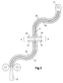
- One such device is the subject of a co-pending German patent application filed on 23 February 2000 by Robert Bosch GmbH and is as shown in Figure 2.
- the balun of Figure 2 consists of two three-line interdigitated sections. Each section is a quarter-wavelength long.
- the first and third lines 20, 21 of the first section are grounded at the unbalanced input port 22 and the other ends of the first and third lines are the terminals 23, 24 of the balanced ports A and B.
- the first and the third lines 25, 26 of the second section are grounded at one end 27, while the second end of these lines are the terminals 28, 29 of the balanced ports A and B.
- the central line 15 is connected at one end to the unbalanced port 22 and is left unterminated at the other end.
- the potentials at the four balanced port terminals of this dual balun are suitable for driving elements connected to the four diodes of a star mixer, for example.
- MMIC microwave monolithic integrated circuit
- balun as recited in Claim 1.
- the balun according to the invention is employed respectively as part of a single-sideband mixer arrangement, as recited in Claim 5, and as part of a downconverter arrangement, as recited in Claim 11. Specific embodiments of the balun, mixer and downconverter are covered by the subclaims.
- a dual balun comprises seven lines 30-36, each having a length equal to a quarter-wavelength at the mean frequency of operation of the balun.
- the central line 33 forms at one end the connection point for the unbalanced port 37 (Port 1) and is terminated at its other end by a connection to ground.
- First and second balanced ports (Ports 2 and 3, respectively) are formed from the corresponding ends of lines 30, 32 and lines 34, 36, respectively. The other end of lines 32 and 34 are grounded.
- Sandwiched between the lines making up each balanced port is a further line (lines 31 and 35) which is grounded at the balanced-port end.
- the unbalanced-port ends of lines 30 and 36 are connected by similar strip sections to the corresponding ends of lines 31 and 35, respectively, while the unbalanced-port ends of lines 31, 33 and 35 are coupled together by means of airbridges 37.
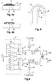
- FIGs 4a and 4b The formation of an airbridge is illustrated in Figures 4a and 4b.
- Figure 4a the lines 31, 32 and 33 shown in Figure 3 are shown in cross-section on a substrate 60.
- a photoresist 62 is deposited onto the substrate and a metallisation interconnect 61 is, in turn, deposited onto the photoresist 62 and the microstrips 31 and 33.
- the photoresist 62 is etched away to leave a airgap 63 (see Figure 4b).
- An alternative to the use of an airbridge is the use of a bypass interconnect, as illustrated in Figure 5.
- a bypass track 64 is deposited onto the substrate (not shown) carrying the strips 30-36 using the thin-film manufacturing technique.
- the embodiment illustrated in Figure 3 shows symmetry of line width (parameter w ) and line spacing (parameter s ) between the two halves of the balun centred on line 33.
- This measure provides equal power distribution between the balanced ports. If unequal distribution were to be required in a particular application, then these parameters may be made to differ between the two halves.
- the actual values of line width and line spacing will be determined by the need to match the balun to the driving and driven circuitry to which it is connected, in accordance with principles well known to those skilled in the art. In practice, these dimensions may well be determined using spectral-domain techniques described in the paper "Spectral Domain Emittance Approach for Dispersion Characteristics of Generalised Printed Transmission Lines" by T.
- balun As regards the coupling of the balun to external circuitry, it may be employed as a matching network interfacing with other circuitry, as well as a balun as such. In this case it will also act as an impedance transformer.
- FIG. 6 An application of the balun according to the present invention is depicted in Figure 6.
- block 40 represents the dual balun described above having lines 30-36 configured to form Ports 1, 2 and 3 as shown in Figure 3.
- the balanced ports, Ports 2 and 3, each feed an arrangement of two diodes connected in series. These are diodes 41 and 42 for Port 2 and diodes 43 and 44 for Port 3.
- the junctions 45, 46 of the two diode arrangements are taken to the inputs of respective low-pass filters 47, 48 and to the inputs of repective high-pass filters 49, 50.
- the outputs of the low-pass filters form the IF input ports 51, 52 of the mixer. Thus these filters isolate the ports 51, 52 from high frequencies within the mixer.
- Input 51 is an in-phase signal, while input 52 is in quadrature thereto. There therefore appear at the inputs of the high-pass filters 49, 50 a pair of sidebands of frequency f LO + f IF , f LO - f IF and f LO + f IF + 90°, f LO + f IF + 90°, respectively.
- the outputs of the high-pass filters (which may conveniently be constituted by simple capacitors) are fed into a 90-degree hybrid coupler, which in the illustrated example is a Lange coupler 53.
- the Lange coupler is used to separate the upper sideband 54 from the lower sideband 55.
- the sideband outputs are unbalanced, like the local-oscillator input port, Port 1.
- the low-pass filter should preferably have at least 20dB attenuation for the local-oscillator and RF signals and less than 0.3dB attenuation for the IF signals.
- the high-pass filter should preferably have 20dB attenuation for the IF signals and less than 0.3dB attenuation for the local-oscillator and RF signals.
- the low-pass filters 47 and 48 may also pass the DC voltage levels necessary to bias the diodes.
- the filters 47, 48 may take the form of spiral inductors or multiple-pole filters, depending on the bandwidth of the IF signals.
- the same circuit can be employed as a down converter.
- a suitable circuit arrangement is shown in Figure 7, in which the mixer circuit shown in Figure 6 is represented by a functional block 70. This time, however, what were the IF inputs of the mixer are now outputs feeding an additional 90° IF-hybrid 71.
- the outputs 54, 55 of the 90° hybrid (e.g. Lange coupler) in the former mixer are now inputs taken to an RF input signal and a ground-referenced load 72, respectively.
- one of the outputs of the 90° hybrid 71 forms an IF output for the downconverter arrangement, while the other output is terminated in a matching load 73. (The image frequency of the RF input appears at this output and is absorbed in the load).
- the local oscillator input (LO) of the former mixer (block 70) continues to be the local oscillator input for the downconverter.
- balun, mixer and downconverter described can be implemented in MIC (microwave integrated circuit) or MMIC (monolithic microwave integrated circuit) technology.
Landscapes
- Superheterodyne Receivers (AREA)
- Toys (AREA)
- Chair Legs, Seat Parts, And Backrests (AREA)
- Transmitters (AREA)
- Coils Or Transformers For Communication (AREA)
- Percussion Or Vibration Massage (AREA)
- Amplitude Modulation (AREA)
Abstract
Description
- The invention relates to a balun and a mixer and a downconverter incorporating such balun.
- It is known to use baluns to provide transitions between symmetrical and unsymmetrical transmissions lines. With a symmetrical line, a signal being carried by the line does not have ground as a reference potential. By contrast, an unsymmetrical line is referenced on one side to ground, so that a signal carried by such a line does have ground as a reference potential. Baluns as described are often used in the input or output stages of double balanced mixers or modulators, etc.
- A balun which consists of four mutually coupled planar lines is known from DE 197 29 761 A1 and is illustrated in Figure 1. This balun has two
couplers planar lines coupler 1 being arranged in an open circuit configuration and coupler 2 in a short-circuit configuration. The two quarter-wavelength long couplers are connected together to provide a three-port balun having aconnection 3 for unsymmetrical signals and twoconnections coupler 1 theopposite ends 6, 7 of the two lines are unterminated. The other end 8 of one line (206) constitutes asymmetrical connection 4, while theother end 9 of the other line (208) is connected to one end of the close-circuit configured line coupler 2.Twoopposite ends other end 12 of one of the lines (220) forms afurther connection 5 for symmetrical signals. The two interconnected ends of the two line couplers form the connectingport 3 for unsymmetrical signals. To achieve a tight coupling (e.g. 3dB) between the lines, the balun is made using multilayer technology. Hence the manufacturing costs are high, which is a problem for the mass-production of, for example, GaAs monolithic integrated circuits. - The balun just described is a single balun and therefore cannot be used in star mixers and modulators and single-sideband mixers. For this purpose it is necessary to use a dual balun. One such device is the subject of a co-pending German patent application filed on 23 February 2000 by Robert Bosch GmbH and is as shown in Figure 2.
- The balun of Figure 2 consists of two three-line interdigitated sections. Each section is a quarter-wavelength long. The first and
third lines unbalanced input port 22 and the other ends of the first and third lines are theterminals third lines end 27, while the second end of these lines are theterminals central line 15 is connected at one end to theunbalanced port 22 and is left unterminated at the other end. The potentials at the four balanced port terminals of this dual balun are suitable for driving elements connected to the four diodes of a star mixer, for example. It consists of purely planar coupled structures and can be realised in single-layer printed-circuit technology. It has the drawback that it is a half-wavelength long in total and therefore takes up a lot of space on a microwave monolithic integrated circuit (MMIC) of which it is intended to form a part. - In accordance with a first aspect of the invention, there is provided a balun as recited in
Claim 1. Under second and third aspects of the invention, the balun according to the invention is employed respectively as part of a single-sideband mixer arrangement, as recited inClaim 5, and as part of a downconverter arrangement, as recited inClaim 11. Specific embodiments of the balun, mixer and downconverter are covered by the subclaims. - An embodiment of the first aspect of the invention will now be described, by way of example only, with reference to the drawings, of which:
- Figure 1 is a schematic diagram of a known single balun;
- Figure 2 is a schematic diagram of a known dual balun;
- Figure 3 is a schematic diagram of a dual balun in accordance with the present invention;
- Figure 4 is cross-sectional diagram showing the construction of an airbridge interconnect;
- Figure 5 is a plan view of a microstrip layout incorporating a bypass interconnect;
- Figure 6 is a circuit diagram of a monolithic single-sideband mixer incorporating a dual balun according to the invention, and
- Figure 7 is a circuit diagram of a downconverter incorporating a dual balun in accordance with the invention.
-
- Referring now to Figure 3, a dual balun according to the present invention comprises seven lines 30-36, each having a length equal to a quarter-wavelength at the mean frequency of operation of the balun. The
central line 33 forms at one end the connection point for the unbalanced port 37 (Port 1) and is terminated at its other end by a connection to ground. First and second balanced ports (Ports lines lines lines lines 31 and 35) which is grounded at the balanced-port end. Finally, the unbalanced-port ends oflines lines lines airbridges 37. - The formation of an airbridge is illustrated in Figures 4a and 4b. In Figure 4a the
lines substrate 60. To form the airbridge aphotoresist 62 is deposited onto the substrate and ametallisation interconnect 61 is, in turn, deposited onto thephotoresist 62 and themicrostrips photoresist 62 is etched away to leave a airgap 63 (see Figure 4b). An alternative to the use of an airbridge is the use of a bypass interconnect, as illustrated in Figure 5. Here abypass track 64 is deposited onto the substrate (not shown) carrying the strips 30-36 using the thin-film manufacturing technique. - The embodiment illustrated in Figure 3 shows symmetry of line width (parameter w) and line spacing (parameter s) between the two halves of the balun centred on
line 33. This measure provides equal power distribution between the balanced ports. If unequal distribution were to be required in a particular application, then these parameters may be made to differ between the two halves. In practice, the actual values of line width and line spacing will be determined by the need to match the balun to the driving and driven circuitry to which it is connected, in accordance with principles well known to those skilled in the art. In practice, these dimensions may well be determined using spectral-domain techniques described in the paper "Spectral Domain Emittance Approach for Dispersion Characteristics of Generalised Printed Transmission Lines" by T. Itoh, IEEE Transactions, MTT-287, July 1980, pp 733-738. As regards the coupling of the balun to external circuitry, it may be employed as a matching network interfacing with other circuitry, as well as a balun as such. In this case it will also act as an impedance transformer. - An application of the balun according to the present invention is depicted in Figure 6. In Figure 6
block 40 represents the dual balun described above having lines 30-36 configured to formPorts Ports diodes Port 2 anddiodes junctions pass filters pass filters IF input ports ports Input 51 is an in-phase signal, whileinput 52 is in quadrature thereto. There therefore appear at the inputs of the high-pass filters 49, 50 a pair of sidebands of frequency fLO + fIF, fLO - fIF and fLO + fIF + 90°, fLO + fIF + 90°, respectively. The outputs of the high-pass filters (which may conveniently be constituted by simple capacitors) are fed into a 90-degree hybrid coupler, which in the illustrated example is aLange coupler 53. The Lange coupler is used to separate theupper sideband 54 from thelower sideband 55. The sideband outputs are unbalanced, like the local-oscillator input port,Port 1. - The low-pass filter should preferably have at least 20dB attenuation for the local-oscillator and RF signals and less than 0.3dB attenuation for the IF signals. Conversely, the high-pass filter should preferably have 20dB attenuation for the IF signals and less than 0.3dB attenuation for the local-oscillator and RF signals.
- Sufficient isolation between the local-oscillator and RF-input sections of the mixer is ensured by arranging for the diode-pairs to be excited in their odd mode. (This makes
Port 1 appear as ground as far as the RF inputs are concerned and makes thediode junctions pass filters filters - In addition to the illustrated mixer arrangement, the same circuit can be employed as a down converter. A suitable circuit arrangement is shown in Figure 7, in which the mixer circuit shown in Figure 6 is represented by a
functional block 70. This time, however, what were the IF inputs of the mixer are now outputs feeding an additional 90° IF-hybrid 71. Likewise, theoutputs matching load 73. (The image frequency of the RF input appears at this output and is absorbed in the load). The local oscillator input (LO) of the former mixer (block 70) continues to be the local oscillator input for the downconverter. - The balun, mixer and downconverter described can be implemented in MIC (microwave integrated circuit) or MMIC (monolithic microwave integrated circuit) technology.
Claims (19)
- A balun, comprising seven adjacently disposed coupled lines (30-36), an unbalanced port (Port 1) and first and second balanced ports (Ports 2 and 3), wherein second, third and fourth of the seven lines (32, 31, 30) lie adjacent each other in sequence on one side of a first of the seven lines (33), with the second line adjacent the first, and fifth, sixth and seventh of the seven lines (34, 35, 36) lie adjacent each other in sequence on the other side of the first line (33), with the fifth line (34) adjacent the first, the lines having corresponding first ends and corresponding second ends, the first end of the first line (33) serving as the unbalanced port (Port 1) and the second end of the first line (33) being connected to a ground reference, the first ends of the first, third, fourth, sixth and seventh lines (33, 31, 30, 35, 36) being connected to each other by conductive interconnect means (37), the second ends of the third and sixth lines (31, 35) being connected to a ground reference, the first ends of the second and fifth lines (32, 34) being connected to a ground reference, the second ends of the second and fourth lines (32, 30) serving as the first balanced port and the second ends of the fifth and seventh lines (34, 36) serving as the second balanced port.
- Balun according to Claim 1, wherein the coupled length of each of the lines is approximately equal to one-quarter of the average operating wavelength of the balun.
- Balun according to Claim 1 or Claim 2, wherein one or more of the interconnect means is an airbridge.
- Balun according to any one of the preceding claims, wherein one or more of the interconnect means is a bypass.
- Single-sideband mixer arrangement comprising a balun according to any one of the preceding claims.
- Mixer arrangement according to Claim 5, wherein the unbalanced port (Port 1) is connected to a local-oscillator source (LO); the first and second balanced ports (Ports 1 and 2) are connected to respective first and second diode-mixer arrangements (41, 42; 43, 44); an output (45) of the first diode-mixer arrangement is connected to a first RF input port (51) and to a first input of a 90° hybrid and an output (46) of the second diode-mixer arrangement is connected to a second RF input port (52) and to a second input of the 90° hybrid, first and second outputs of the 90° hybrid constituting the upper-sideband and lower-sideband outputs, respectively, of the mixer arrangement.
- Mixer arrangement according to Claim 6, wherein each of the diode-mixer arrangements comprises a pair of diodes connected in series across the relevant balanced port, the diode-mixer output being constituted by the junction between the two diodes.
- Mixer arrangement as claimed in Claim 6 or Claim 7, wherein the connections between the diode-mixer arrangements and the RF ports are by way of respective low-pass filters (47, 48).
- Mixer arrangement according to any one of Claims 6 to 8, wherein the connections between the diode-mixer arrangements and the 90°-hybrid inputs are by way of respective high-pass filters (49, 50).
- Mixer arrangement according to any one of Claims 5 to 9, wherein the 90° hybrid is a Lange coupler (53).
- Downconverter arrangement, comprising a balun according to any one of Claims 1 to 4.
- Downconverter arrangement according to Claim 11, wherein the unbalanced port is connected to a local-oscillator source (LO); the first and second balanced ports are connected to respective first and second diode-mixer arrangements (41, 42; 43, 44); an output (45) of the first diode-mixer arrangement is connected to a first IF output port (51) and to a first output of a first 90° hybrid (53) and an output (46) of the second diode-mixer arrangement is connected to a second IF output port (52) and to a second output of the first 90° hybrid (53); a first input (54) of the first 90° hybrid constitutes the RF input port of the downconverter and a second input of the first 90° hybrid is terminated by a load (72), the first and second IF output ports (51, 52) being connected to first and second inputs, respectively, of a second 90° hybrid (71), a first output of the second 90° hybrid constituting the IF output port of the downconverter and a second output of the second 90° hybrid being terminated by a load (73).
- Downconverter arrangement according to Claim 12, wherein each of the diode-mixer arrangements comprises a pair of diodes (41, 42; 43, 44) connected in series across the relevant balanced port, the diode-mixer output being constituted by the junction (45, 46) between the two diodes.
- Downconverter arrangement as claimed in Claim 12 or Claim 13, wherein the connections between the diode-mixer arrangements and the IF ports are by way of respective low-pass filters (47, 48).
- Downconverter arrangement according to any one of Claims 12 to 14, wherein the connections between the diode-mixer arrangements and the outputs of the first 90° hybrid (53) are by way of respective high-pass filters (49, 50).
- Downconverter arrangement according to any one of Claims 12 to 15, wherein the first and/or second 90° hybrid (53, 71) is a Lange coupler.
- Balun substantially as shown in, or as hereinbefore described with reference to, Figures 3-5 of the drawings.
- Single-sideband mixer arrangement as shown in, or as hereinbefore described with reference to, Figure 6 of the drawings.
- Downconverter arrangement as shown in, or as hereinbefore described with reference to, Figure 7 of the drawings.
Priority Applications (6)
| Application Number | Priority Date | Filing Date | Title |
|---|---|---|---|
| EP00117612A EP1184931B1 (en) | 2000-08-16 | 2000-08-16 | A balun and a mixer and downconverter incorporating same |
| DE60031399T DE60031399T2 (en) | 2000-08-16 | 2000-08-16 | Symmetriereinrichtung, mixer and thus provided down converter |
| AT00117612T ATE343227T1 (en) | 2000-08-16 | 2000-08-16 | BALANCER DEVICE, MIXER AND DOWNWARD CONVERTER PROVIDED WITH IT |
| US09/928,254 US20020022458A1 (en) | 2000-08-16 | 2001-08-10 | Balun and a mixer and downconverter incorporating same |
| NO20013976A NO20013976L (en) | 2000-08-16 | 2001-08-15 | Balloon and mixes and down converts where included |
| CN01125425.4A CN1340910A (en) | 2000-08-16 | 2001-08-15 | Balance-unbalance inverter, heterodyne modulator and lower frequency converter using them |
Applications Claiming Priority (1)
| Application Number | Priority Date | Filing Date | Title |
|---|---|---|---|
| EP00117612A EP1184931B1 (en) | 2000-08-16 | 2000-08-16 | A balun and a mixer and downconverter incorporating same |
Publications (2)
| Publication Number | Publication Date |
|---|---|
| EP1184931A1 true EP1184931A1 (en) | 2002-03-06 |
| EP1184931B1 EP1184931B1 (en) | 2006-10-18 |
Family
ID=8169537
Family Applications (1)
| Application Number | Title | Priority Date | Filing Date |
|---|---|---|---|
| EP00117612A Expired - Lifetime EP1184931B1 (en) | 2000-08-16 | 2000-08-16 | A balun and a mixer and downconverter incorporating same |
Country Status (6)
| Country | Link |
|---|---|
| US (1) | US20020022458A1 (en) |
| EP (1) | EP1184931B1 (en) |
| CN (1) | CN1340910A (en) |
| AT (1) | ATE343227T1 (en) |
| DE (1) | DE60031399T2 (en) |
| NO (1) | NO20013976L (en) |
Cited By (1)
| Publication number | Priority date | Publication date | Assignee | Title |
|---|---|---|---|---|
| JPWO2005076404A1 (en) * | 2004-02-06 | 2008-01-10 | 株式会社村田製作所 | Balanced distributor |
Families Citing this family (5)
| Publication number | Priority date | Publication date | Assignee | Title |
|---|---|---|---|---|
| JPWO2005064787A1 (en) * | 2003-12-25 | 2007-07-26 | 株式会社アドバンテスト | Frequency converter |
| JP2009260444A (en) * | 2008-04-11 | 2009-11-05 | Toshiba Corp | Power combiner, amplifier, and transmitter |
| CN102818963B (en) * | 2012-09-11 | 2014-09-17 | 上海电缆研究所 | BALUN-free multichannel symmetrical data cable testing method and system |
| CN104022322B (en) * | 2013-03-01 | 2016-08-03 | 国基电子(上海)有限公司 | Balun |
| CN109891667A (en) | 2016-10-27 | 2019-06-14 | 瑞典爱立信有限公司 | Balun device |
Citations (3)
| Publication number | Priority date | Publication date | Assignee | Title |
|---|---|---|---|---|
| US4186352A (en) * | 1978-03-23 | 1980-01-29 | Rockwell International Corporation | Signal converter apparatus |
| US4739289A (en) * | 1986-11-24 | 1988-04-19 | Celeritek Inc. | Microstrip balun having improved bandwidth |
| US5121090A (en) * | 1990-04-09 | 1992-06-09 | Tektronix, Inc. | Balun providing dual balanced outputs |
Family Cites Families (3)
| Publication number | Priority date | Publication date | Assignee | Title |
|---|---|---|---|---|
| US5697088A (en) * | 1996-08-05 | 1997-12-09 | Motorola, Inc. | Balun transformer |
| FI103614B (en) * | 1997-03-20 | 1999-07-30 | Nokia Mobile Phones Ltd | Phasing and balancing means |
| US6351192B1 (en) * | 1999-03-25 | 2002-02-26 | Industrial Technology Research Institute | Miniaturized balun transformer with a plurality of interconnecting bondwires |
-
2000
- 2000-08-16 EP EP00117612A patent/EP1184931B1/en not_active Expired - Lifetime
- 2000-08-16 AT AT00117612T patent/ATE343227T1/en not_active IP Right Cessation
- 2000-08-16 DE DE60031399T patent/DE60031399T2/en not_active Expired - Lifetime
-
2001
- 2001-08-10 US US09/928,254 patent/US20020022458A1/en not_active Abandoned
- 2001-08-15 NO NO20013976A patent/NO20013976L/en unknown
- 2001-08-15 CN CN01125425.4A patent/CN1340910A/en active Pending
Patent Citations (3)
| Publication number | Priority date | Publication date | Assignee | Title |
|---|---|---|---|---|
| US4186352A (en) * | 1978-03-23 | 1980-01-29 | Rockwell International Corporation | Signal converter apparatus |
| US4739289A (en) * | 1986-11-24 | 1988-04-19 | Celeritek Inc. | Microstrip balun having improved bandwidth |
| US5121090A (en) * | 1990-04-09 | 1992-06-09 | Tektronix, Inc. | Balun providing dual balanced outputs |
Non-Patent Citations (1)
| Title |
|---|
| RYU Y I ET AL: "A MONOLITHIC BROADBAND DOUBLY BALANCED EHF HBT STAR MIXER WITH NOVEL MICROSTRIP BALUNS", IEEE MTT-S INTERNATIONAL MICROWAVE SYMPOSIUM DIGEST,US,NEW YORK, IEEE, 16 May 1995 (1995-05-16), pages 119 - 122, XP000538554, ISBN: 0-7803-2582-6 * |
Cited By (2)
| Publication number | Priority date | Publication date | Assignee | Title |
|---|---|---|---|---|
| JPWO2005076404A1 (en) * | 2004-02-06 | 2008-01-10 | 株式会社村田製作所 | Balanced distributor |
| US7468640B2 (en) | 2004-02-06 | 2008-12-23 | Murata Manufacturing Co., Ltd. | Balanced splitter |
Also Published As
| Publication number | Publication date |
|---|---|
| EP1184931B1 (en) | 2006-10-18 |
| US20020022458A1 (en) | 2002-02-21 |
| NO20013976L (en) | 2002-02-19 |
| ATE343227T1 (en) | 2006-11-15 |
| NO20013976D0 (en) | 2001-08-15 |
| DE60031399T2 (en) | 2007-08-30 |
| CN1340910A (en) | 2002-03-20 |
| DE60031399D1 (en) | 2006-11-30 |
Similar Documents
| Publication | Publication Date | Title |
|---|---|---|
| EP0927434B1 (en) | Thick film construct for quadrature translation of rf signals | |
| US5105171A (en) | Coplanar waveguide directional coupler and flip-clip microwave monolithic integrated circuit assembly incorporating the coupler | |
| Kord et al. | Low-loss broadband magnetless circulators for full-duplex radios | |
| US6351192B1 (en) | Miniaturized balun transformer with a plurality of interconnecting bondwires | |
| EP0322612B1 (en) | Microwave image suppression harmonic frequency converter | |
| EP1184931B1 (en) | A balun and a mixer and downconverter incorporating same | |
| EP0081818B1 (en) | Microwave integrated circuit frequency converter | |
| Zhang et al. | Multifunctional filtering circuits: 3D multifunctional filtering circuits based on high-Q dielectric resonators and coaxial resonators | |
| US20060208828A1 (en) | DC isolated phase inverter and a ring hybrid coupler including the DC isolated phase inverter | |
| US5339462A (en) | Broadband mixer circuit and method | |
| JP4343374B2 (en) | Single balance mixer | |
| JPH0462481B2 (en) | ||
| EP0068870B1 (en) | Microwave integrated circuit mixer | |
| US6275689B1 (en) | Double-balanced mixer | |
| Ogawa et al. | K-band integrated double-balanced mixer | |
| US4371982A (en) | Microwave frequency converter with economical coupling | |
| JP2897676B2 (en) | Mixer circuit | |
| KR19990000905A (en) | Frequency converters for use in microwave systems | |
| US4392251A (en) | Symmetric microwave mixer with coplanar diode connection | |
| US4392250A (en) | Symmetric microwave mixer | |
| US3634768A (en) | Wide bandwidth microwave mixer circuits | |
| US4380831A (en) | Symmetric microwave mixer with improved isolation | |
| Knochel et al. | Unilateral microstrip balanced and doubly balanced mixers | |
| US4399562A (en) | Full balun mixer | |
| US4375699A (en) | Microwave frequency converter with dual balun port |
Legal Events
| Date | Code | Title | Description |
|---|---|---|---|
| PUAI | Public reference made under article 153(3) epc to a published international application that has entered the european phase |
Free format text: ORIGINAL CODE: 0009012 |
|
| AK | Designated contracting states |
Kind code of ref document: A1 Designated state(s): AT BE CH CY DE DK ES FI FR GB GR IE IT LI LU MC NL PT SE |
|
| AX | Request for extension of the european patent |
Free format text: AL;LT;LV;MK;RO;SI |
|
| 17P | Request for examination filed |
Effective date: 20020823 |
|
| AKX | Designation fees paid |
Free format text: AT BE CH CY DE DK ES FI FR GB GR IE IT LI LU MC NL PT SE |
|
| GRAP | Despatch of communication of intention to grant a patent |
Free format text: ORIGINAL CODE: EPIDOSNIGR1 |
|
| GRAS | Grant fee paid |
Free format text: ORIGINAL CODE: EPIDOSNIGR3 |
|
| GRAA | (expected) grant |
Free format text: ORIGINAL CODE: 0009210 |
|
| AK | Designated contracting states |
Kind code of ref document: B1 Designated state(s): AT BE CH CY DE DK ES FI FR GB GR IE IT LI LU MC NL PT SE |
|
| PG25 | Lapsed in a contracting state [announced via postgrant information from national office to epo] |
Ref country code: AT Free format text: LAPSE BECAUSE OF FAILURE TO SUBMIT A TRANSLATION OF THE DESCRIPTION OR TO PAY THE FEE WITHIN THE PRESCRIBED TIME-LIMIT Effective date: 20061018 Ref country code: CH Free format text: LAPSE BECAUSE OF FAILURE TO SUBMIT A TRANSLATION OF THE DESCRIPTION OR TO PAY THE FEE WITHIN THE PRESCRIBED TIME-LIMIT Effective date: 20061018 Ref country code: FI Free format text: LAPSE BECAUSE OF FAILURE TO SUBMIT A TRANSLATION OF THE DESCRIPTION OR TO PAY THE FEE WITHIN THE PRESCRIBED TIME-LIMIT Effective date: 20061018 Ref country code: BE Free format text: LAPSE BECAUSE OF FAILURE TO SUBMIT A TRANSLATION OF THE DESCRIPTION OR TO PAY THE FEE WITHIN THE PRESCRIBED TIME-LIMIT Effective date: 20061018 Ref country code: LI Free format text: LAPSE BECAUSE OF FAILURE TO SUBMIT A TRANSLATION OF THE DESCRIPTION OR TO PAY THE FEE WITHIN THE PRESCRIBED TIME-LIMIT Effective date: 20061018 |
|
| REG | Reference to a national code |
Ref country code: GB Ref legal event code: FG4D |
|
| REG | Reference to a national code |
Ref country code: CH Ref legal event code: EP Ref country code: IE Ref legal event code: FG4D |
|
| REF | Corresponds to: |
Ref document number: 60031399 Country of ref document: DE Date of ref document: 20061130 Kind code of ref document: P |
|
| REG | Reference to a national code |
Ref country code: GB Ref legal event code: 732E |
|
| PG25 | Lapsed in a contracting state [announced via postgrant information from national office to epo] |
Ref country code: DK Free format text: LAPSE BECAUSE OF FAILURE TO SUBMIT A TRANSLATION OF THE DESCRIPTION OR TO PAY THE FEE WITHIN THE PRESCRIBED TIME-LIMIT Effective date: 20070118 Ref country code: SE Free format text: LAPSE BECAUSE OF FAILURE TO SUBMIT A TRANSLATION OF THE DESCRIPTION OR TO PAY THE FEE WITHIN THE PRESCRIBED TIME-LIMIT Effective date: 20070118 |
|
| PG25 | Lapsed in a contracting state [announced via postgrant information from national office to epo] |
Ref country code: ES Free format text: LAPSE BECAUSE OF FAILURE TO SUBMIT A TRANSLATION OF THE DESCRIPTION OR TO PAY THE FEE WITHIN THE PRESCRIBED TIME-LIMIT Effective date: 20070129 |
|
| RAP2 | Party data changed (patent owner data changed or rights of a patent transferred) |
Owner name: ERICSSON AB |
|
| PG25 | Lapsed in a contracting state [announced via postgrant information from national office to epo] |
Ref country code: PT Free format text: LAPSE BECAUSE OF FAILURE TO SUBMIT A TRANSLATION OF THE DESCRIPTION OR TO PAY THE FEE WITHIN THE PRESCRIBED TIME-LIMIT Effective date: 20070319 |
|
| REG | Reference to a national code |
Ref country code: CH Ref legal event code: PL |
|
| NLT2 | Nl: modifications (of names), taken from the european patent patent bulletin |
Owner name: ERICSSON AB Effective date: 20070307 |
|
| ET | Fr: translation filed | ||
| NLS | Nl: assignments of ep-patents |
Owner name: ERICSSON AB Effective date: 20070319 |
|
| PLBE | No opposition filed within time limit |
Free format text: ORIGINAL CODE: 0009261 |
|
| STAA | Information on the status of an ep patent application or granted ep patent |
Free format text: STATUS: NO OPPOSITION FILED WITHIN TIME LIMIT |
|
| 26N | No opposition filed |
Effective date: 20070719 |
|
| PGFP | Annual fee paid to national office [announced via postgrant information from national office to epo] |
Ref country code: IT Payment date: 20070830 Year of fee payment: 8 |
|
| PG25 | Lapsed in a contracting state [announced via postgrant information from national office to epo] |
Ref country code: MC Free format text: LAPSE BECAUSE OF NON-PAYMENT OF DUE FEES Effective date: 20070831 Ref country code: GR Free format text: LAPSE BECAUSE OF FAILURE TO SUBMIT A TRANSLATION OF THE DESCRIPTION OR TO PAY THE FEE WITHIN THE PRESCRIBED TIME-LIMIT Effective date: 20070119 |
|
| PG25 | Lapsed in a contracting state [announced via postgrant information from national office to epo] |
Ref country code: IE Free format text: LAPSE BECAUSE OF NON-PAYMENT OF DUE FEES Effective date: 20070816 |
|
| PG25 | Lapsed in a contracting state [announced via postgrant information from national office to epo] |
Ref country code: CY Free format text: LAPSE BECAUSE OF FAILURE TO SUBMIT A TRANSLATION OF THE DESCRIPTION OR TO PAY THE FEE WITHIN THE PRESCRIBED TIME-LIMIT Effective date: 20061018 Ref country code: LU Free format text: LAPSE BECAUSE OF NON-PAYMENT OF DUE FEES Effective date: 20070816 Ref country code: IT Free format text: LAPSE BECAUSE OF NON-PAYMENT OF DUE FEES Effective date: 20080816 |
|
| PGFP | Annual fee paid to national office [announced via postgrant information from national office to epo] |
Ref country code: DE Payment date: 20140827 Year of fee payment: 15 |
|
| PGFP | Annual fee paid to national office [announced via postgrant information from national office to epo] |
Ref country code: GB Payment date: 20140827 Year of fee payment: 15 Ref country code: FR Payment date: 20140818 Year of fee payment: 15 |
|
| REG | Reference to a national code |
Ref country code: DE Ref legal event code: R082 Ref document number: 60031399 Country of ref document: DE Representative=s name: BURCHARDI, THOMAS, DIPL.-ING. UNIV., DE |
|
| PGFP | Annual fee paid to national office [announced via postgrant information from national office to epo] |
Ref country code: NL Payment date: 20150826 Year of fee payment: 16 |
|
| REG | Reference to a national code |
Ref country code: DE Ref legal event code: R119 Ref document number: 60031399 Country of ref document: DE |
|
| GBPC | Gb: european patent ceased through non-payment of renewal fee |
Effective date: 20150816 |
|
| REG | Reference to a national code |
Ref country code: FR Ref legal event code: ST Effective date: 20160429 |
|
| PG25 | Lapsed in a contracting state [announced via postgrant information from national office to epo] |
Ref country code: GB Free format text: LAPSE BECAUSE OF NON-PAYMENT OF DUE FEES Effective date: 20150816 Ref country code: DE Free format text: LAPSE BECAUSE OF NON-PAYMENT OF DUE FEES Effective date: 20160301 |
|
| PG25 | Lapsed in a contracting state [announced via postgrant information from national office to epo] |
Ref country code: FR Free format text: LAPSE BECAUSE OF NON-PAYMENT OF DUE FEES Effective date: 20150831 |
|
| REG | Reference to a national code |
Ref country code: NL Ref legal event code: MM Effective date: 20160901 |
|
| PG25 | Lapsed in a contracting state [announced via postgrant information from national office to epo] |
Ref country code: NL Free format text: LAPSE BECAUSE OF NON-PAYMENT OF DUE FEES Effective date: 20160901 |