EP1184901A1 - Method of manufacturing semiconductor integrated circuit having multilayer wiring structure - Google Patents
Method of manufacturing semiconductor integrated circuit having multilayer wiring structure Download PDFInfo
- Publication number
- EP1184901A1 EP1184901A1 EP01906202A EP01906202A EP1184901A1 EP 1184901 A1 EP1184901 A1 EP 1184901A1 EP 01906202 A EP01906202 A EP 01906202A EP 01906202 A EP01906202 A EP 01906202A EP 1184901 A1 EP1184901 A1 EP 1184901A1
- Authority
- EP
- European Patent Office
- Prior art keywords
- test
- integrated circuit
- testing
- semiconductor integrated
- fabricating
- Prior art date
- Legal status (The legal status is an assumption and is not a legal conclusion. Google has not performed a legal analysis and makes no representation as to the accuracy of the status listed.)
- Withdrawn
Links
Images







Classifications
-
- H—ELECTRICITY
- H10—SEMICONDUCTOR DEVICES; ELECTRIC SOLID-STATE DEVICES NOT OTHERWISE PROVIDED FOR
- H10P—GENERIC PROCESSES OR APPARATUS FOR THE MANUFACTURE OR TREATMENT OF DEVICES COVERED BY CLASS H10
- H10P74/00—Testing or measuring during manufacture or treatment of wafers, substrates or devices
-
- H—ELECTRICITY
- H10—SEMICONDUCTOR DEVICES; ELECTRIC SOLID-STATE DEVICES NOT OTHERWISE PROVIDED FOR
- H10P—GENERIC PROCESSES OR APPARATUS FOR THE MANUFACTURE OR TREATMENT OF DEVICES COVERED BY CLASS H10
- H10P74/00—Testing or measuring during manufacture or treatment of wafers, substrates or devices
- H10P74/23—Testing or measuring during manufacture or treatment of wafers, substrates or devices characterised by multiple measurements, corrections, marking or sorting processes
Definitions
- the present invention relates to a method for fabricating semiconductor integrated circuit dies with multi-layered interconnect structures.
- a semiconductor integrated circuit of a high integration level comprises a plurality of stacked interconnect layers to define a plurality of sub-circuits having a variety of functions after primitive devices have been formed.
- Fig. 1 there is shown a semiconductor integrated circuit having a plurality of sub-circuits.
- Sub-circuits may be large scale functional blocks such as CPU, memory, DSP, AD converter, I/O interface or the like, or may be relatively small scale or basic sub-circuits such as adder, multiplier, multiplexer, flip-flop or the like.
- the functional blocks and sub-circuits may be digital circuits, analog circuits or mixed signal circuits.
- the semiconductor integrated circuit A has a multi-layered interconnect structure comprising a plurality of interconnect layers (N-layers as shown in Fig. 2).
- a lowermost layer (the first interconnect layer) provides a wiring connection between primitive devices ( transistors ) formed in a semiconductor substrate, and is the interconnect layer which defines a basic logic gate, which is an NAND gate or an inverter in the example shown, as shown in Fig. 3.
- Input and output signal lines for the basic logic gates appear on the stacking surface of the first interconnect layer. Shown within blocks of this Figure which are indicated in broken lines are primitive devices, which do not appear on the surface of the first interconnect layer.
- the second interconnect layer provides a wiring connection between the basic logic gates which are formed by the first interconnect layer, and is the interconnect layer which defines relatively small scale sub-circuits as illustrated in Fig. 4, for example. Input and output signal lines for the sub-circuit appear on the surface of the second interconnect layer, but logic gates or inverters which constitute such circuits do not appear there.
- the i-th interconnect layer (3 ⁇ i ⁇ N-1) provides a wiring connection between sub-circuits which have been formed up to the (i-1)-th interconnect layer, and is the interconnect layer which defines sub-circuits of a higher scale, and input and output signal lines for the sub-circuits of the higher scale appear on the stacking surface of the i-th interconnect layer.
- N-th interconnect layer provides a wiring connection between sub-circuits (S1, S2, ⁇ , Sk) which are formed by the (N-1)-th interconnect layer, and is the interconnect layer which defines a semiconductor integrated circuit A. Only input and output signal lines for the semiconductor integrated circuit A appear on the stacking surface of the N-th interconnect layer, as shown in Fig. 5.
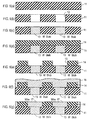
- Stacking of individual interconnect layers takes place in a manner shown in Fig. 6. While not shown, a product from an immediately preceding step, namely a substrate in which primitive devices are formed or an immediately preceding interconnect layer is initially subject to a deposition thereon of an oxide layer 11 such as formed by SiO 2 , as shown in Fig. 6 (a). Photolithography is applied to the oxide layer 11 to define a mask for junctions with wirings or primitive devices located directly below it, and then the reactive ion etching (RIE) technique is applied to form openings 12, as shown in Fig. 6 (b). The openings 12 are then filled with a conductive material, for example, tungsten to form junctions (stubs) 13, as shown in Fig. 6 (c).
- RIE reactive ion etching
- an oxide layer 14 as formed by SiO 2 is deposited. Photolithography is applied to the oxide layer 14 to define a mask and the reactive ion etching (RIE) technique is applied to form grooves 15 for regions to be wired, as indicated in Fig. 6 (e).
- RIE reactive ion etching
- a layer 16 of a metal such as Al, W, Cu or the like is formed as shown in Fig. 6 (f), and the metal layer 16 is then subject to a chemical-mechanical polishing (CMP) to expose the oxide layer 14.
- Wires 17 which fill the grooves 15 form a wiring 17 which is connected to the junctions 13 and also connected to the underlying interconnect layer, not shown, through the junctions 13.
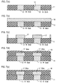
- Steps to stack an interconnect layer may follow a procedure shown in Fig. 7.
- a condition as shown in Fig. 7 (a) is prepared in which junctions 13 fill in an oxide layer 11.
- a metal layer 16 is formed over the entire surface as shown in Fig. 7 (b), and the application of the photolithography and the RIE technique form wires 17 connected to the junctions 13, as shown in Fig. 7 (c).
- An oxide layer 18 is then deposited over the entire surface as shown in Fig. 7 (d), and the surface of the oxide layer 18 is planarized by CMP, as shown in Fig. 7 (e).
- CMP planarized by CMP
- a method for fabricating a semiconductor integrated circuit with a multi-layered interconnect structure has been briefly described above.
- a conventional method for fabricating a semiconductor integrated circuit there has been no practice of testing primitive devices or sub-circuits which have been already formed in the course of the fabricating steps.
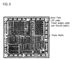
- a test of the semiconductor integrated circuit has taken place by placing a probe in contact with bonding pads of a chip as shown in Fig. 8 after the steps of fabricating a semiconductor integrated circuit chip have been completed to provide an IC in a wafer condition, inputting externally a test pattern to input pads on the circuit under test, and observing a voltage response signal on a power supply pad of the circuit under test or a current response signal through a power supply pad of the circuit under test( wafer probing, die sort).
- a test pattern is externally input to an input terminal (pin) of the circuit under test and a voltage response signal on an output terminal (pin) of the circuit under test or a current response signal through a power supply terminal (pin) of the circuit under test is observed to perform a test of the semiconductor integrated circuit (package test or final test).
- Such tests will be hereafter referred to as final tests.
- a final test of the semiconductor integrated circuit utilizes a stuck-at fault test, a delay fault test, a quiescent power supply current (IDDQ) test, a functional test, an exhaustive test and the like.
- the stuck-at fault test is a procedure which assumes a stuck-at fault on a signal line in the circuit under test (which is a fault where a logical signal value on the signal line is fixed to a certain value; a fault in which the signal value is fixed to "0" is referred to as stuck-at 0 fault while a fault in which the signal value is fixed to "1” is referred to as stuck-at 1 fault) by seeing an influence of a fault through the observation of a voltage signal on an output terminal of the circuit under test with respect to a given test pattern.
- the delay fault test is a procedure which assumes a delay fault in a signal propagation path or a logical gate in the circuit under test, or a fault that a time interval required for a signal to propagate through the signal propagation path or the logical gate (delay time) exceeds or undershoots a given value (a delay fault in the signal propagation path being referred to as a path delay fault and a delay fault in the logical gate as a gate delay fault), by seeing an influence of a fault through the observation of a voltage transition signal on an output terminal of the circuit under test with respect to a given series of test patterns.
- the quiescent power supply current test is a procedure which assumes a short-circuit fault across a plurality of signal lines in the circuit under test or a leak fault in a primitive device therein by seeing an influence of a fault through the observation of a quiescent current signal through a power supply terminal of the circuit under test with respect to a given test pattern.
- the functional test is a procedure which examines whether or not the circuit under test functions properly.
- the exhaustive test is a procedure which examines output responses of the circuit under test for every combination of signal values to input terminals and flip-flops of the circuit under test. For the stuck-at fault test and the functional test, a description is given, for example, in chapters 6 and 8 of M. Abramovici, M.A. Breuer and A.D.
- test facilitating design technique which affords testing functions to the circuit under test such as the technique of built-in self test (BIST) function into the circuit under test, the test point insertion which is intended to improve the controllability and the observability of an internal status of the circuit, the scan design technique, the boundary scan and the like.
- BIST built-in self test
- a description of the test facilitating design techniques is given, for example, in chapters 9, 10 and 11 of M. Abramovivi, M. A. Breuer and A. D. Friedman, Digital Systems Testing and Tastable Design, IEEE Press, New York, 1990.
- the prior art procedure of testing the semiconductor integrated circuit by the final test involves problems that it is impossible to detect a poor work or a poor function which occurs during fabricating steps, that it is difficult to identify a sub-system which is highly likely to give rise to a fault, and that it is difficult to acquire data on a device level or a sub-system level which are useable in a simulation or a modelling which is intended for purpose of improving a system performance.
- the test facilitating design technique while allowing an external access to be dispensed with or simplified and facilitating a testing of the circuit under test, suffers from drawbacks of an increased overhead for the chip area, a degradation in the performance of the semiconductor integrated circuit under test which is caused by a testing circuit, a fault coverage which is less than desired, an increased length of time required for the test, etc.
- a method for fabricating a semiconductor integrated circuit with a multi-layered interconnect structure by repeating a step of stacking interconnect layers (an interconnect layer stacking step) a plurality of times after primitive devices have been formed is characterized by the inclusion of a testing step of successively testing one or more sub-circuits which have been interconnected up to at least one or more intermediate interconnect layer stacking steps among the plurality of the interconnect layer stacking steps.
- testing step in the fabricating method for the invention be conducted such that during a first testing step, one or more sub-circuits which have been interconnected up to the preceding stacking step be tested, and during a subsequent testing step, the interconnection between the sub-circuits be tested.
- testing step in the fabricating method for the invention be conducted such that during a relatively early testing step of a given stack stage, one or more sub-circuits of a relatively small scale which have been interconnected by preceding stacking steps be tested, and during a subsequent testing step for the final layer, a final functional test of an integrated circuit which is finally interconnected be conducted.
- the fabricating method according to the invention includes a CMP (chemical mechanical polishing) planarizing step to planarize a stacking surface before transferring into a succeeding stacking step subsequent to the testing step.
- CMP chemical mechanical polishing
- the fabricating method according to the invention includes a testing of the semiconductor integrated circuit by using the test facilitating design technique in the testing step, and a subsequent removal of a wiring to a testing circuit of the test facilitating design technique which is used in the testing step.
- the fabricating method according to the invention comprises a step of confirming whether or not a given step has been completed upon termination of an interconnect layer stacking step, transferring to the testing step if the completion has been confirmed, and transferring to a next stacking step if the completion has not been completed; and a step of confirming whether or not the steps of fabricating a semiconductor integrate circuit have been completed upon termination of the testing step and transferring to a next stacking step when the completion is not found.
- the fabricating method according to the invention comprises a step of confirming whether or not a given step has been completed upon termination of a stacking step, transferring to a first testing step which tests a plurality of primitive devices or sub-circuits which have been formed and interconnected up to the given step when the completion is found, and transferring to a next stacking step when the completion is not found; a step of transferring to a next stacking step subsequent to the first testing step; a step of confirming whether or not a given interconnect layer stacking step has been completed after the first testing step, transferring to a second testing step which tests an interconnection for a plurality of wirings between the plurality of sub-circuits which have been connected up to the given stacking step when the completion is found, and transferring to a stacking step which follows the first testing step when the completion is not found; and a step of confirming whether or not steps of fabricating a semiconductor integrated circuit have been completed, and transferring to a stacking step which follows the first testing step when the completion is not found;
- a test is conducted by placing a probe in contact with a signal line or lines appearing on the stacking surface by using a probing means such as a probe card or the like.
- a probing means such as a probe card or the like.
- a test for the level of larger scale sub-circuits on the stacking surface of an i-th interconnect layer as shown in Fig.
- a test of an overall semiconductor integrated circuit takes place on the stacking surface of an N-th interconnect layer.
- a test for the level of primitive devices or a measurement of element parameters of primitive devices may take place by placing a probe in contact with a substrate.
- a suitable value may be chosen for the number N of the interconnected layers depending on the scale and the layered structure of the circuit.
- testing cost for a semiconductor integrated circuit can be reduced.
- the testing cost will be represented here in terms of the number of test patterns.
- the exhaustive test is a procedure which tests output responses of a circuit under test for every combination of signal values at input terminals of the circuit under test and at flip-flops.
- the semiconductor integrated circuit B comprises combinatorial circuits C1, C2, C3, C4 which do not contain flip-flops and m flip-flops circuits F1, F2, ⁇ , Fm, all of which represents sub-circuits. Assume that the semiconductor integrated circuit B has a number of input terminals which is equal to t, and the combinatorial circuits or sub-circuits C1, C2, C3, C4 have numbers of input signal lines which are equal to p, q, r, s, respectively (in the example shown in Fig.
- N (Bsub) 2 p +2 q +2 r +2 s +8 m Accordingly, the number of test patterns in the testing step which is employed in the method for fabricating a semiconductor integrated circuit according to the invention can be reduced from the number of test patterns in the conventional test for the semiconductor integrated circuit by an amount given below.
- N (B) - N (Bsub) 2 t+m - (2 p + 2 q + 2 r + 2 s + 8 m ).
- N(B)-N(Bsub) will be positive.
- the method for fabricating a semiconductor integrated circuit it is only needed that after a test for the level of sub-circuits is conducted, the sub-circuits be tested whether they are properly interconnected in the testing step for each interconnect layer up to the uppermost layer. Since it is only required to test the interconnection of the wiring under test by observing the propagated logical signal value, the number of test patterns which are required to perform such test is sufficiently small as compared with the number of test patterns which are used during the test of sub-circuits.
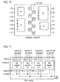
- the 16 bit counter has four 4bit counters S1, S2, S3 and S4 as sub-circuits.
- effect of reducing the testing cost will be more remarkably manifest for a larger scale circuit.
- effect is not limited to the exhaustive test or the functional test, but a similar effect can also be obtained for the stuck-at fault test, the delay fault test, the quiescent power supply current test, the transient power supply current test and the like.
- each sub-circuit is tested separately during the testing step, when a plurality of sub-circuits are formed, these plural sub-circuits may be tested in parallel, thus allowing the testing time to be further reduced. Since the sub-circuit operate independently from each other unless they are wired together as shown in Fig. 4, a parallel test can be made by placing probes simultaneously in contact with a plurality of sub-circuits which appear on the same stacking surface.
- the interposition of a testing step between intermediate multi-layer stacking steps allows the fault coverage to be improved and the reliability of the semiconductor integrated circuit to be improved.
- the integration level of the circuit is increased, the number of stuck-at faults which are subject to the stuck-at fault test increases, and this combined with the presence of flip-flops in a sequential circuit renders an access to faulty locations within the circuit difficult.
- a testing circuit for the level of sub-circuits may be interposed under condition that smaller scale sub-circuits are formed during an intermediate fabricating step, thereby allowing a stuck-at fault test to be conducted for each sub-circuit within an practical length of time and thus allowing the fault coverage for the stuck-at faults for the entire circuit to be improved.
- CMOS integrated circuit As the miniaturization of circuit elements ( MOS transistors) proceeds and the circuit tends to be integrated at a higher level, a leak current from a transistor increases, and accordingly, a quiescent power supply current for the entire chip increases, making it difficult to detect an increase in the quiescent power supply current which is caused by a single fault. Accordingly, the quiescent power supply current test is very difficult to perform in the larger scale CMOS integrated circuit.
- MOS transistors MOS transistors
- a test for the level of sub-circuits may be performed under a condition that smaller scale sub-circuits are formed, thereby allowing the quiescent power supply current test to be conducted for each sub-circuit and allowing the rate for detecting short-circuit faults and/or leakage faults over the entire circuit to be improved.
- Such effect is not limited to the stuck-at fault test or the quiescent power supply current test, but a similar effect can be obtained with respect to the delay fault test, the functional test, the exhaustive test, the transient power supply current test and the like as well.
- a test interposed during the steps of fabricating a circuit enables an early detection of poor works such as disconnection faults or short-circuit faults and/or malfunctioning which results in an out-of-specification circuit performance, and a subsequent testing step or fabricating steps may be eliminated therefor, thus allowing the testing cost and the fabricating cost for the semiconductor integrated circuit to be reduced.
- a test can be performed for the level of sub-circuit at the point when the sub-circuits are formed or for the level of sub-systems at the point when these sub-systems (relatively larger scale sub-circuits) are formed to allow a sub-system or sub-systems to be identified which are highly likely to give rise to a failure, and such information can be utilized to the incorporation of the test facilitating design technique, the scan design technique or the built-in self test (BIST) technique or to improving the reliability of the entire system, thereby allowing a system repair interval of an increased length ( a time interval required to repair a faulty system into a normal system) to be reduced.
- test facilitating design techniques a description is given, for example, in chapters 9, 10, 11 of M. Abramovici, M. A. Breuer and A. D. Friedman, Digital Systems Testing and Testable Design, IEEE Press, New York, 1990.
- a simulation or a modeling to improve a system performance requires the acquisition of performance data such as delay times or current driving capabilities on a device level or on a sub-system level.
- performance data such as delay times or current driving capabilities on a device level or on a sub-system level.
- the method for fabricating a semiconductor integrated circuit according to the invention allows an appropriate test to be applied to the sub-circuit level, thus avoiding the need to insert a testing circuit according to the test facilitating design techniques into the integrated circuit and thus allowing an area overhead which may be caused by such testing circuit to be reduced.
- the method for fabricating a semiconductor integrated circuit according to the invention allows, by an effective utilization of CMP ( chemical mechanical polishing ) planarizing step, a degradation in the performance of the semiconductor integrated circuit which may be caused by the inserted testing circuit to be prevented if the test facilitating design technique is incorporated.
- CMP chemical mechanical polishing
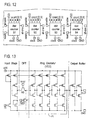
- a test facilitating design technique as shown in Fig. 13 has been proposed in order to facilitate a testing of a phase-locked loop ( PLL).
- PLL phase-locked loop
- a description of this procedure is described, for example, in F. Azais, M. Renovell, Y. Bertrand, A. Ivanov, and S. Tabatabaei, "A Unified Digital Test Technique for PLLs : Catastrophic Fault Covered, "Proceedings of 5th IEEE International Mixed Signal Testing Workshop, pp. 269-292, June 1999.
- MOSFET M1 is turned ON while MOSTET M2 is turned OFF, and an input to an output buffer is inputted to the input stage of the oscillator circuit, or a feedback loop FL is closed to form the VCO circuit.
- MOSFET (M1) is inserted in the feedback loop FL of the VCO circuit according to this procedure, a problem is presented that a resistance of MOSFET lowers the operational speed of the PLL circuit during the normal operation.
- a testing step may be interposed by placing a probe in contact with the wiring in the PLL under test to turn M1 OFF and to turn M2 ON in order to perform a test of the PLL circuit under test, and after the PLL circuit under test has been tested, the wiring to the testing circuit M1 and M2 shown in broken lines may be removed by CMP and a wiring L1 shown in solid line may be stacked anew, as shown in Fig, 14, thus reconfiguring a feedback loop in which M1 is removed, thus allowing a PLL circuit which is free from a degradation in the performance to be fabricated.
- an interconnect layer which comprises wirings shown in dotted lines in Fig. 14 is formed to provide a circuit arrangement shown in Fig. 13 to perform a test, and upon completion of the test, the interconnected layers shown in dotted lines is removed, and an interconnect layer which forms the wiring L 1 to define the feedback loop is formed thereon.
- the reconfigured PLL circuit is already tested, and there is an assurance that it operates normally.
- a test facilitating design technique as illustrated in Fig. 15 is also proposed to facilitate the delay fault test and the stuck-at fault test of a digital integrated circuit.
- This procedure is described, for example, in K. Arabi, H. Ihs, C. Dufaza and B. Kaminska, "Digital Oscillation-Test Method for Delay and Stuck-at Fault testing of Digital Circuits, " Proceedings of IEEE International Test Conference, pp.91-100, Oct. 1999.
- This procedure comprises connecting an input signal line L2 and an output signal line L4 of a signal propagation path under test of a digital integrated circuit (or more generally, a critical path having a longest delay time is selected) through an XOR gate and a multiplexer in loop form as indicated in thick lines.
- an input TEST of the multiplexer is controlled so that the feedback loop is deactivated, thus connecting B 1 to L2 to operate the circuit under test while during the test, the multiplexer MUX is controlled to connect the output of the XOR gate to the input line L2 to define the loop, and input INV of the XOR gate is controlled to form a ring oscillator including an odd number of output inverting logical gates ( output inverting gates ) within the loop, thus testing the delay fault and the stuck-at fault on the critical path.
- the XOR gate is used to control the number of output inverting gates on the feedback loop by providing "1" for the input INV to operate it as an output inverting gate when there is even number of output inverting gates on the critical path while providing "0" for the input INV when there are an odd number of output inverting gates on the critical path.
- a testing step is executed under a condition that an interconnect layer which connects the testing circuit MUX, XOR is formed.
- a probe is placed in contact with the wiring in the digital semiconductor integrated circuit, a required input is applied to test the digital semiconductor integrated circuit, and subsequently, the testing circuit shown in dotted lines as shown in Fig. 16, namely, the interconnect layer leading to MUX and XOR is removed by CMP while an input signal line which is shown in a thick solid line is stacked anew.
- a semiconductor integrated circuit with a multi-layered interconnect structure which is subject to the fabrication according to the invention comprises a damascene interconnect structure.
- a damascene interconnect structure is described, for example, in A. K. Stamper, T. L. McDevitt, and S. L. Luce, "Sub-0.25-micron Interconnection Scaling : Damascene Copper versus Subtractive Aluminum, " IEEE/SEMI Advanced Semiconductor Manufacturing Conference, pp. 337-346, 1998.
- a wiring material is not limited to the copper (Cu), but may comprise copper-magnesium (Cu-Mg) or any other material.
- a semiconductor integrated circuit with a damascene interconnect structure is subject, subsequent to a given stacking step and before entering a succeeding stacking step, to a step of planarizing the stacking surface as shown in Fig. 6 (g), for example, to a CMP planarizing step.
- the planarizing step allows a miniscule scar of contact such as a minute dimple, which may be formed when a probe is placed in contact therewith during the testing step at an intermediate stage, which defines an essential feature of the invention, to be removed. Accordingly, the testing step which takes place during the fabricating steps can be implemented without any influence upon the steps of fabricating a semiconductor integrated circuit.
- a semiconductor integrated circuit with a multi-layered interconnect structure which is subject to the fabrication according to the invention is not limited to a digital circuit, but may comprise an analog circuit or a mixed signal circuit comprising a mixture of a digital circuit and an analog circuit.
- a semiconductor integrated circuit with a multi-layered interconnect structure which is subject to fabrication according to the present invention is not limited to single substrate semiconductor integrated circuit, but may comprise a semiconductor integrated circuit which is implemented in three dimensions by stack of a plurality of sub-substrates.
- a semiconductor integrated circuit with a multi-layered interconnect structure which is subject to the fabrication according to the present invention is not limited to a single chip semiconductor integrated circuit, but may comprise a semiconductor integrated circuit which is formed by integrating a plurality of sub-chips by using a common multi-layer interconnect structure.
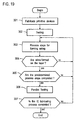
- Fig. 17 shows an example of a processing procedure of the method for fabricating a semiconductor integrated circuit according to the invention.
- a step of forming primitive devices such as transistors
- a confirmation is made to see whether or not signal lines are formed on a layer surface, and if they are not formed, an interconnect layer stacking step shown at step 103 is used to form signal lines, and if the signal lines are formed, the operation proceeds to step 104.
- step 104 a confirmation is made to see whether or not at least one given step which is predetermined during the fabrication is completed, and if the given step is not completed, the interconnect layer stacking step at step 103 is repeated, and if the given step has been completed, the operation proceeds to step 105.
- the interconnect layer stacking step at step 103 comprises a step of stacking a interconnect layer for primitive devices and sub-circuits, and may comprise process steps shown in Fig. 6, for example.
- step 105 a plurality of primitive devices or sub-circuits which have been formed and wired together up to said step are tested either sequentially or in parallel.
- step 106 a confirmation is made to see whether or not the steps of fabricating a semiconductor integrated circuit have been completed. If the fabricating steps have not been completed, the steps 102, 103, 104 and 105 are repeated, and if the fabricating steps have been completed, the processing is completed.
- the testing step at step 105 may comprise a test for primitive devices, a test for smaller sub-circuits, a test for the relatively larger sub-circuits or the like, depending on the interconnection which has been completed up to that point and takes place each time each interconnect layer such as the second and a subsequent interconnect layer is formed.
- the test of primitive devices or sub-circuits may use an exhaustive test, a functional test, a stuck-at fault test, a delay fault test, a quiescent power supply power current test, a transient power supply current test, a parametric test or any other testing method.
- a test which takes place after the formation of each interconnect layer which follows the initial test may comprise only a wiring connection test.
- Fig. 18 shows another example of a processing procedure of the method for fabricating a semiconductor integrated circuit according to the invention.
- a step of forming primitive devices such as transistors
- a confirmation is made to see whether or not signal lines are formed on the surface of the interconnect layer, and if the signal lines are not formed, the signal lines are formed by an interconnect layer stacking step (first half), at step 203, which may comprise a process shown in Figs. 7(a) ⁇ (c), for example, and if the signal lines are formed, the operation proceeds to step 204.
- step 204 a confirmation is made to see whether or not a given step (not limited to one) has been completed, and if the given step has not been completed, the operation proceeds to an interconnect stacking step (second half) of step 206.
- an interconnect layer stacking step (second half) which may comprise a process shown in Figs. 7(d), (e) is performed to complete the interconnecting step.
- a test of primitive devices or sub-circuits may use an exhausive test, a functional test, a stuck-at fault test, a delay fault test, a quiescent power supply current test, a transient power supply current test, a parametric test, a wiring connection test or any other testing method.
- Fig. 19 shows a further example of a processing procedure of the method for fabricating a semiconductor integrated circuit according to the invention.
- a step of forming primitive devices such as transistors
- a test for the level of primitive devices or a parametric test which measures the element parameters of primitive devices takes place.
- signal lines are formed by an interconnect layer stacking step, and at step 304, a confirmation is made to see whether or not the signal lines are formed on the stacking surface, and if the signal lines are not formed, the operation returns to step 303, while if the signal lines are formed, the operation proceeds to step 305.
- a confirmation is made to see whether or not a given step (not limited to one) has been completed. If the given step has not been completed, an interconnect layer stacking step at step 303 is repeated, while if the given step has been completed, the operation proceeds to step 306.
- the interconnect layer stacking step at step 303 is one where an interconnect layer for the primitive devices or sub-circuits is formed by stacking, and which may comprise process steps as shown in Fig. 6, for example.
- step 306 a plurality of primitive devices or sub-circuits which have been formed and wired together up to this point are tested either sequentially or in parallel.
- a confirmation is made to see whether or not the steps of fabricating a semiconductor integrated circuit have been completed, and if the fabricating steps have not been completed, the steps 303, 304, 305 and 306 are repeated. However, if the fabricating steps have been completed, the processing is completed.
- a test of primitive devices or sub-circuits may use an exhaustive test, a functional test, a stuck-at fault test, a delay fault test, a quiescent power supply current test, a transient power supply current test, a parametric test, a wiring connection test or any other testing method.
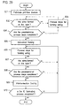
- Fig. 20 shows an additional example of a processing procedure of the method for fabricating a semiconductor integrated circuit according to the invention.
- a step of forming primitive devices such as transistors
- a confirmation is made to see whether or not signal lines are formed on the stacking surface, and if the signal lines are not formed, the signal lines are formed by the interconnect layer stacking step of step 503, while if the signal lines are formed, the operation proceeds to step 504.
- a confirmation is made to see whether or not a given step has been completed and if the given step has not been completed, the interconnect layer stacking step of step 503 is repeated, while if the given step has been completed, the operation proceeds to step 505.
- the interconnect layer stacking step of step 503 is one where the interconnect layer for the primitive devices or sub-circuits is formed by stacking and which may comprise the process steps shown in Fig. 6, for example.
- step 505 a test of the plurality of primitive devices or sub-circuits which have been formed and wired together up to this point takes place.
- the interconnect layer stacking step of step 506 is a step of forming an interconnect layer which wires together the plurality of primitive devices or sub-circuits that have been tested up to the step 505 to form a larger scale sub-circuit, and may comprise process steps shown in Fig. 6, for example.
- a confirmation is made to see whether or not signal lines are formed on the stacking surface, and if the signal lines are not formed, the interconnect layer stacking step of step 506 is used to form the signal lines. However, if the signal lines are formed, the operation proceeds to step 508.
- step 508 a confirmation is made to see whether or not a given stacking step (which is not limited to one) has been completed, and if the given stacking step has not been completed, the stacking step of step 506 is repeated, while if the given stacking step has been completed, the operation proceeds to step 509.
- step 509 a wiring connection test takes place with respect to a plurality of wirings extending between a plurality of sub-circuits which have been connected together up to the stacking step.
- a confirmation is made to see whether or not the steps of fabricating a semiconductor integrated circuit have been completed, and if the fabricating steps have not been completed, the steps 506, 507, 508 and 509 are repeated, while if the fabricating steps have been completed, the processing is completed.
- a test of the primitive devices or sub-circuits may use an exhaustive test, a functional test, a stuck-at fault test, a delay fault test, a quiescent power supply current test, a transient power supply current test, a parametric test or any other testing method.
- the sub-circuit testing step of step 505 may test the plurality of sub-circuits sequentially, or may test them in parallel.
- the wiring connection testing step of step 509 may test the plurality of wiring connections sequentially or may test them in parallel. It is preferred that the wiring connection test of step 509 be conducted each time an interconnect layer stacking step which follows the step 505 has been completed. In this instance, step 508 may be omitted.
- Fig. 21 shows still another example of a processing procedure of the method for fabricating a semiconductor integrated circuit according to the invention.
- a step of forming primitive devices such as transistors
- a confirmation is made to see whether or not signal lines are formed on the stacking surface, and if the signal lines are not formed, the operation proceeds to an interconnect layer stacking step of step 605, while if the signal lines are formed, the operation proceeds to step 603.
- step 603 a confirmation is made to see whether or not a given step (which is not limited to one) has been completed, and if the given step has not been completed, the operation proceeds to the interconnect layer stacking step of step 605, while if the given step has been completed, the operation proceeds to step 604.
- step 604 a test of the plurality of primitive devices or sub-circuits which have been formed and wired together up to this point takes place.
- step 605 an interconnect layer stacking step takes place, thus forming signal lines on the surface of the interconnect layer.
- the interconnect layer stacking step of step 605 is one in which a wiring between the primitive devices or sub-circuit is made by stacking, and which may comprise process steps shown in Fig. 6, for example.
- step 606 a confirmation is made to see whether or not the steps of fabricating a semiconductor integrated circuit have been completed, and if the fabricating steps have not been completed, the steps 602, 603, 604 and 605 are repeated, while if the fabricating steps have been completed, the operation proceeds to step 607.
- step 607 a final functional test (functional test) of finally integrated semiconductor integrated circuit takes place to complete the processing.
- a test of the primitive devices or sub-circuits may use an exhaustive test, a functional test, a stuck-at fault test, a delay fault test, a quiescent power supply current test, a transient power supply current test, a parametric test or any other testing method.
- the sub-circuits testing step of step 604 may test the plurality of sub-circuits sequentially or may test them in parallel.
- the final functional testing step of step 606 may use a testing method other than the functional test, as required.
- the final test of step 607 may take place by placing a probe in contact with a bonding pad on the semiconductor integrated circuit, or may take place with respect to a packaged semiconductor integrated circuit.
- Fig. 22 shows a still further example of a processing procedure of the method for fabricating a semiconductor integrated circuit according to the invention.
- a step of forming primitive devices such as transistors
- a confirmation is made to see if signal lines are formed on the stacking surface, and if the signal lines are not formed, an interconnect layer stacking step of step 803 is used to form the signal lines, while if the signal lines are formed, the operation proceeds to step 804.
- step 804 a confirmation is made to see whether or not a given step (which is not limited to one) has been completed, and if the given step has not been completed, the interconnect layer stacking step of step 803 is repeated, while if the given step has been completed, the operation proceeds to step 805.
- a given step which is not limited to one
- the interconnect layer stacking step of step 803 is one in which the wiring for the primitive devices or sub-circuits is formed by stacking and which may comprise process steps shown in Fig. 6, for example.
- step 805 a test of the plurality of primitive devices or sub-circuits which have been formed and wired together up to this point takes place.
- step 806 a CMP planarizing step takes place.
- Purpose of CMP planarizing step 806 is to remove minuscule scars of contact which may be formed when a probe is placed in contact at the testing step 805 or to remove a wiring to the testing circuit used for the test facilitating design technique which may have been used in the testing step 805.
- step 807 a confirmation is made to see whether or not the steps of fabricating a semiconductor integrated circuit have been completed, and if the fabricating steps have not been completed, the steps 802, 803, 804, 805 and 806 are repeated, while if the fabricating steps have been completed, the processing is completed.
- the test of the primitive devices or the sub-circuits may use an exhaustive test, a functional test, a stuck-at fault test, a delay fault test, a quiescent power supply current test, a transient power supply current test, a parametric test, a wiring connection test or any other testing method.
- the testing step of step 805 may test the plurality of sub-circuits sequentially or may test them in parallel.
- the interconnect layer stacking step in each of steps 503 and 506 in Fig. 20, the step 605 in Fig. 21 and the step 803 in Fig. 22 may use a process shown in Fig. 7.
- the interconnect layer stacking step may be divided into a first half step and a second half step, as shown in the embodiment of Fig. 18, and where the test takes place at a given step, it may take place after the completion of the first half step, and may be followed by the second half step.
- a test for the level of sub-circuits may be performed in the course of fabricating a semiconductor integrated circuit with a multi-layered interconnect structure, thus allowing the number of test patterns and the testing cost to be reduced to provide a significant improvement in the economical effect of a large scale semiconductor integrated circuit testing.
- a test for the level of sub-circuits in the course of steps of manufacturing a semiconductor integrated circuit with a multi-layered interconnect structure allows a testing method which would be inapplicable to a large scale integrated circuit to be used, thus significantly improving a fault coverage.
- a test for the level of sub-circuits in the course of fabricating a semiconductor integrated circuit with a multi-layered interconnect structure dispenses with the test facilitating design technique which may be used to improve the ease of testing sub-circuits, allowing an area overhead for the testing circuit to be reduced to null.
- a test for the level of sub-circuits in the course of fabricating a semiconductor integrated circuit with a multi-layered interconnect structure enables a parallel testing of wirings between the sub-circuits or between a system and sub-circuits located on the same chip as the system functions, thus allowing a testing time interval and a testing cost to be reduced and allowing a semiconductor integrated circuit which is free from faults to be fabricated in a reduced length of time.
- a test for the level of sub-circuits in the course of fabricating a semiconductor integrated circuit with a multi-layered interconnect structure enables an early detection of poor works such as disconnection faults or short-circuit faults and malfunctioning which would cause an out-of-specification circuit performance, thus allowing a testing cost and a fabricating cost for the semiconductor integrated circuit to be reduced.
- a test for the level of sub-circuits in the course of fabricating a semiconductor integrated circuit with a multi-layered interconnect structure allows sub-systems which are highly likely to cause failures to be identified, and such information may be used to incorporate the test facilitating design technique or to improve the reliability of the overall system, thus allowing a system repair interval of an increased length ( a time interval required to repair a faulty system into a normal system) to be reduced.
- a test for the level of sub-circuits in the course of fabricating a semiconductor integrated circuit with a multi-layered interconnect structure enables the acquisition of performance data such as delay times or current driving capabilities on the device level or the sub-system level which would be necessary in the simulation or modeling to improve the system performance.
- a test for the level of sub-circuits in the course of manufacturing a semiconductor integrated circuit with a multi-layered interconnect structure enables that the assurance for acceptable components be given which satisfy KGD (known good die) standard demands upon the final test, thus allowing KGD cost to be significantly reduced.
- the wiring for the testing circuit which is used in the testing step may be removed by utilizing CMP ( chemical mechanical polishing ) planarizing step to reconfigure the circuit, thus preventing a degradation in the performance of the semiconductor integrated circuit under test which may be caused by the test facilitating design technique from occuring.
- CMP chemical mechanical polishing
Landscapes
- Semiconductor Integrated Circuits (AREA)
- Testing Or Measuring Of Semiconductors Or The Like (AREA)
- Internal Circuitry In Semiconductor Integrated Circuit Devices (AREA)
Abstract
In a method for fabricating an LSI in which primitive devices such as
transistors are formed on a semiconductor substrate and a plurality of
interconnect layers are formed thereover to provide sub-circuits of
successively larger scale and increasing complexity including sub-circuits
which are formed by a connection of the primitive devices and sub-circuits of
a larger scale which are formed by a connection of the sub-circuits, under a
condition that an intermediate interconnect layer is formed, an exhaustive test,
a functional test, a stuck-at fault test, a quiescent power supply current test or
the like takes place with respect to the primitive devices or the sub-circuits
which are wired together by the intermediate interconnect layer, and
subsequently, a wiring connection test takes place after the formation of each
subsequent interconnect layer. A fault coverage is improved while a testing
cost and a fabricating cost are reduced.
Description
The present invention relates to a method for fabricating
semiconductor integrated circuit dies with multi-layered interconnect
structures.
A semiconductor integrated circuit of a high integration level
comprises a plurality of stacked interconnect layers to define a plurality of
sub-circuits having a variety of functions after primitive devices have been
formed.
In Fig. 1, there is shown a semiconductor integrated circuit having a
plurality of sub-circuits. A semiconductor integrated circuit A shown has a
plurality of sub-circuits S1, S2, ···, Sk (k=6 in the example shown in Fig.
2). Sub-circuits may be large scale functional blocks such as CPU, memory,
DSP, AD converter, I/O interface or the like, or may be relatively small scale
or basic sub-circuits such as adder, multiplier, multiplexer, flip-flop or the like.
In addition, the functional blocks and sub-circuits may be digital circuits,
analog circuits or mixed signal circuits.
The semiconductor integrated circuit A has a multi-layered
interconnect structure comprising a plurality of interconnect layers (N-layers
as shown in Fig. 2). A lowermost layer (the first interconnect layer) provides
a wiring connection between primitive devices ( transistors ) formed in a
semiconductor substrate, and is the interconnect layer which defines a basic
logic gate, which is an NAND gate or an inverter in the example shown, as
shown in Fig. 3. Input and output signal lines for the basic logic gates
appear on the stacking surface of the first interconnect layer. Shown within
blocks of this Figure which are indicated in broken lines are primitive devices,
which do not appear on the surface of the first interconnect layer. The
second interconnect layer provides a wiring connection between the basic
logic gates which are formed by the first interconnect layer, and is the
interconnect layer which defines relatively small scale sub-circuits as
illustrated in Fig. 4, for example. Input and output signal lines for the
sub-circuit appear on the surface of the second interconnect layer, but logic
gates or inverters which constitute such circuits do not appear there. The i-th
interconnect layer (3 ≦ i ≦ N-1) provides a wiring connection between
sub-circuits which have been formed up to the (i-1)-th interconnect layer, and
is the interconnect layer which defines sub-circuits of a higher scale, and
input and output signal lines for the sub-circuits of the higher scale appear on
the stacking surface of the i-th interconnect layer. An uppermost layer (N-th
interconnect layer) provides a wiring connection between sub-circuits (S1,
S2, ···, Sk) which are formed by the (N-1)-th interconnect layer, and is the
interconnect layer which defines a semiconductor integrated circuit A. Only
input and output signal lines for the semiconductor integrated circuit A appear
on the stacking surface of the N-th interconnect layer, as shown in Fig. 5.
Stacking of individual interconnect layers takes place in a manner
shown in Fig. 6. While not shown, a product from an immediately preceding
step, namely a substrate in which primitive devices are formed or an
immediately preceding interconnect layer is initially subject to a deposition
thereon of an oxide layer 11 such as formed bySiO 2 , as shown in Fig. 6 (a).
Photolithography is applied to the oxide layer 11 to define a mask for
junctions with wirings or primitive devices located directly below it, and then
the reactive ion etching (RIE) technique is applied to form openings 12, as
shown in Fig. 6 (b). The openings 12 are then filled with a conductive
material, for example, tungsten to form junctions (stubs) 13, as shown in Fig.
6 (c). As shown in Fig. 6 (d), an oxide layer 14 as formed by SiO 2 is
deposited. Photolithography is applied to the oxide layer 14 to define a
mask and the reactive ion etching (RIE) technique is applied to form grooves
15 for regions to be wired, as indicated in Fig. 6 (e). A layer 16 of a metal
such as Al, W, Cu or the like is formed as shown in Fig. 6 (f), and the metal
layer 16 is then subject to a chemical-mechanical polishing (CMP) to expose
the oxide layer 14. Wires 17 which fill the grooves 15 form a wiring 17
which is connected to the junctions 13 and also connected to the underlying
interconnect layer, not shown, through the junctions 13.
Steps to stack an interconnect layer may follow a procedure shown in
Fig. 7. In a similar manner as illustrated in Fig. 6, a condition as shown in
Fig. 7 (a) is prepared in which junctions 13 fill in an oxide layer 11.
Subsequently, a metal layer 16 is formed over the entire surface as shown in
Fig. 7 (b), and the application of the photolithography and the RIE technique
form wires 17 connected to the junctions 13, as shown in Fig. 7 (c). An
oxide layer 18 is then deposited over the entire surface as shown in Fig. 7 (d),
and the surface of the oxide layer 18 is planarized by CMP, as shown in Fig. 7
(e). In this instance, when openings 12 are formed to provide the junctions 13,
the openings 12 should contiguously extend to reach the wires in the
underlying interconnect layer.
A method for fabricating a semiconductor integrated circuit with a
multi-layered interconnect structure has been briefly described above. In a
conventional method for fabricating a semiconductor integrated circuit, there
has been no practice of testing primitive devices or sub-circuits which have
been already formed in the course of the fabricating steps.
In other words, a test of the semiconductor integrated circuit has taken
place by placing a probe in contact with bonding pads of a chip as shown in
Fig. 8 after the steps of fabricating a semiconductor integrated circuit chip
have been completed to provide an IC in a wafer condition, inputting
externally a test pattern to input pads on the circuit under test, and observing a
voltage response signal on a power supply pad of the circuit under test or a
current response signal through a power supply pad of the circuit under
test( wafer probing, die sort). Alternatively, a test pattern is externally input
to an input terminal (pin) of the circuit under test and a voltage response
signal on an output terminal (pin) of the circuit under test or a current
response signal through a power supply terminal (pin) of the circuit under test
is observed to perform a test of the semiconductor integrated circuit (package
test or final test). Such tests will be hereafter referred to as final tests.
A final test of the semiconductor integrated circuit utilizes a stuck-at
fault test, a delay fault test, a quiescent power supply current (IDDQ) test, a
functional test, an exhaustive test and the like. The stuck-at fault test is a
procedure which assumes a stuck-at fault on a signal line in the circuit under
test (which is a fault where a logical signal value on the signal line is fixed to
a certain value; a fault in which the signal value is fixed to "0" is referred to
as stuck-at 0 fault while a fault in which the signal value is fixed to "1" is
referred to as stuck-at 1 fault) by seeing an influence of a fault through the
observation of a voltage signal on an output terminal of the circuit under test
with respect to a given test pattern. The delay fault test is a procedure which
assumes a delay fault in a signal propagation path or a logical gate in the
circuit under test, or a fault that a time interval required for a signal to
propagate through the signal propagation path or the logical gate (delay time)
exceeds or undershoots a given value (a delay fault in the signal propagation
path being referred to as a path delay fault and a delay fault in the logical gate
as a gate delay fault), by seeing an influence of a fault through the
observation of a voltage transition signal on an output terminal of the circuit
under test with respect to a given series of test patterns. The quiescent
power supply current test is a procedure which assumes a short-circuit fault
across a plurality of signal lines in the circuit under test or a leak fault in a
primitive device therein by seeing an influence of a fault through the
observation of a quiescent current signal through a power supply terminal of
the circuit under test with respect to a given test pattern. The functional test
is a procedure which examines whether or not the circuit under test functions
properly. The exhaustive test is a procedure which examines output
responses of the circuit under test for every combination of signal values to
input terminals and flip-flops of the circuit under test. For the stuck-at fault
test and the functional test, a description is given, for example, in chapters 6
and 8 of M. Abramovici, M.A. Breuer and A.D. Friedman, Digital Systems
Testing and Testable Design, IEEE Press, New York, 1990; for the delay fault
test, a description is given, for example, in G.L. Smith, "Model for Delay
Faults Based upon Paths," Proceedings of IEEE International Test Conference,
pp. 342-349, 1985 or C.J. Lin and S.M. Reddy, "On Delay Fault Testing in
Logic Circuits, " Transactions on Computer-Aided Design, CAD-6 (5),
pp.694-703, 1987; for the quiescent power supply current test, a description is
given, for example, in S. Chakravarty and P. J. Thadikaran, Intuduction to
IDDQ Testing, Kluwer Academic Publichers, Boston, 1997; and for transient
power supply current test, a description is given, for example, in M. Sachdev,
P. Jamssen. and V. Zieren, "Defect Detection with Transient Current Testing
and its Potential for Deep Submicron ICs, " Proceedings of IEEE
International Test Conference, pp.204-213, 1998 or Y. Min and Z. Li, "IDDT
Testing versus IDDQ testing, "Journal of Electronic Testing : Theory and
Applications (JETTA), vol. 13, No. I, pp. 51-56, August 1998.
In order to facilitate the testing of the circuit under test, use is also
made of a test facilitating design technique, which affords testing functions to
the circuit under test such as the technique of built-in self test (BIST) function
into the circuit under test, the test point insertion which is intended to improve
the controllability and the observability of an internal status of the circuit, the
scan design technique, the boundary scan and the like. A description of the
test facilitating design techniques is given, for example, in chapters 9, 10 and
11 of M. Abramovivi, M. A. Breuer and A. D. Friedman, Digital Systems
Testing and Tastable Design, IEEE Press, New York, 1990.
However, as the circuit integration level rises to a system LSI, for
example, in which a memory, MPU, DSP, I/O interface and the like are
integrated into a single chip, the number of faults which would be subject to
tests such as the stuck-at fault test, the delay fault test and the quiescent power
supply current test will be enormous, prohibiting a testing of all of these faults
in a practicable length of time. In addition, for the exhaustive test, the
number of status corresponding to the number of internal flip-flops increases
as an exponential function, making it very difficult to conduct such test.
Furthermore, as the circuit scale increases, an increase in the number of
functions contained in the circuit under test results in a tremendous figure for
the number of test patterns which are required to test every function in the
circuit under test.
As described above, if it is desired to test functions of the circuit under
test by the final test, an increased length of time is required, and the testing
cost of the final test increases. On the other hand, a large scale integrated
circuit cannot be subject to testing all of the stuck-at faults, delay faults and
short-circuit faults, presenting a problem that a high fault coverage rate
cannnot be obtained.
What is added is the fact that a rate of increase in the number of pins
of an IC package is low in comparison to the rate of improving the integration
level of a semiconductor integrated circuit, and this means that an external
access to signal lines within the circuit will be further difficult in future,
rendering the final test of the semiconductor integrated circuit very expensive.
It is also to be noted that the prior art procedure of testing the
semiconductor integrated circuit by the final test involves problems that it is
impossible to detect a poor work or a poor function which occurs during
fabricating steps, that it is difficult to identify a sub-system which is highly
likely to give rise to a fault, and that it is difficult to acquire data on a device
level or a sub-system level which are useable in a simulation or a modelling
which is intended for purpose of improving a system performance.
On the other hand, the test facilitating design technique, while
allowing an external access to be dispensed with or simplified and facilitating
a testing of the circuit under test, suffers from drawbacks of an increased
overhead for the chip area, a degradation in the performance of the
semiconductor integrated circuit under test which is caused by a testing circuit,
a fault coverage which is less than desired, an increased length of time
required for the test, etc.
Accordingly, there is a need for a testing method which allows the
testing cost to be reduced and a testing method which is capable of achieving
a higher fault coverage for a large scale semiconductor integrated circuit.
It is an object of the present invention to provide a method for
fabricating a semiconductor integrated circuit with a multi-layered
interconnect structure which allows a testing cost to be reduced or which
allows a fault coverage for a circuit under test to be improved.
In accordance with a method according to the invention, a method for
fabricating a semiconductor integrated circuit with a multi-layered
interconnect structure by repeating a step of stacking interconnect layers ( an
interconnect layer stacking step) a plurality of times after primitive devices
have been formed is characterized by the inclusion of a testing step of
successively testing one or more sub-circuits which have been interconnected
up to at least one or more intermediate interconnect layer stacking steps
among the plurality of the interconnect layer stacking steps.
With this method, the cost of testing a circuit can be reduced, the fault
coverage within the circuit can be improved, and a fault-free semiconductor
integrated circuit can be fabricated.
It is desirable that the testing step in the fabricating method for the
invention be conducted such that during a first testing step, one or more
sub-circuits which have been interconnected up to the preceding stacking step
be tested, and during a subsequent testing step, the interconnection between
the sub-circuits be tested.
It is also desirable that the testing step in the fabricating method for
the invention be conducted such that during a relatively early testing step of a
given stack stage, one or more sub-circuits of a relatively small scale which
have been interconnected by preceding stacking steps be tested, and during a
subsequent testing step for the final layer, a final functional test of an
integrated circuit which is finally interconnected be conducted.
It is also desirable that the fabricating method according to the
invention includes a CMP (chemical mechanical polishing) planarizing step to
planarize a stacking surface before transferring into a succeeding stacking
step subsequent to the testing step.
It is also desirable that the fabricating method according to the
invention includes a testing of the semiconductor integrated circuit by using
the test facilitating design technique in the testing step, and a subsequent
removal of a wiring to a testing circuit of the test facilitating design technique
which is used in the testing step.
It is also desirable that the fabricating method according to the
invention comprises a step of confirming whether or not a given step has been
completed upon termination of an interconnect layer stacking step,
transferring to the testing step if the completion has been confirmed, and
transferring to a next stacking step if the completion has not been completed;
and a step of confirming whether or not the steps of fabricating a semiconductor integrate circuit have been completed upon termination of the testing step and transferring to a next stacking step when the completion is not found.
and a step of confirming whether or not the steps of fabricating a semiconductor integrate circuit have been completed upon termination of the testing step and transferring to a next stacking step when the completion is not found.
It is also desirable that the fabricating method according to the
invention comprises a step of confirming whether or not a given step has been
completed upon termination of a stacking step, transferring to a first testing
step which tests a plurality of primitive devices or sub-circuits which have
been formed and interconnected up to the given step when the completion is
found, and transferring to a next stacking step when the completion is not
found; a step of transferring to a next stacking step subsequent to the first
testing step; a step of confirming whether or not a given interconnect layer
stacking step has been completed after the first testing step, transferring to a
second testing step which tests an interconnection for a plurality of wirings
between the plurality of sub-circuits which have been connected up to the
given stacking step when the completion is found, and transferring to a
stacking step which follows the first testing step when the completion is not
found; and a step of confirming whether or not steps of fabricating a
semiconductor integrated circuit have been completed, and transferring to a
stacking step which follows the first testing step when the completion is not
found.
With a method for fabricating a semiconductor integrated circuit
according to the invention, after a given intermediate stacking step or in the
course of such step, a test is conducted by placing a probe in contact with a
signal line or lines appearing on the stacking surface by using a probing
means such as a probe card or the like. For example, a test for the level of
basic logical gates on the stacking surface of a first interconnect layer as
shown in Fig. 9 (a), a test for the level of relatively small scale sub-circuits
on the stacking surface of a second interconnect layer as shown in Fig. 9 (b),
or a test for the level of larger scale sub-circuits on the stacking surface of an
i-th interconnect layer as shown in Fig. 9 (c) may take place, and as required,
a test of an overall semiconductor integrated circuit takes place on the
stacking surface of an N-th interconnect layer. In addition, before the first
interconnect layer is stacked, a test for the level of primitive devices or a
measurement of element parameters of primitive devices may take place by
placing a probe in contact with a substrate. A suitable value may be chosen
for the number N of the interconnected layers depending on the scale and the
layered structure of the circuit.
With the method for fabricating a semiconductor integrated circuit
according to the invention thus constructed, a testing cost for a semiconductor
integrated circuit can be reduced. The testing cost will be represented here
in terms of the number of test patterns.
An exhaustive test for a semiconductor integrated circuit B shown in
Fig. 10 may be considered. The exhaustive test is a procedure which tests
output responses of a circuit under test for every combination of signal values
at input terminals of the circuit under test and at flip-flops. The
semiconductor integrated circuit B comprises combinatorial circuits C1, C2,
C3, C4 which do not contain flip-flops and m flip-flops circuits F1, F2, ···,
Fm, all of which represents sub-circuits. Assume that the semiconductor
integrated circuit B has a number of input terminals which is equal to t, and
the combinatorial circuits or sub-circuits C1, C2, C3, C4 have numbers of
input signal lines which are equal to p, q, r, s, respectively (in the example
shown in Fig. 8, t=7, m=8, p=4, q=3, r=5, s=3). When the circuit is divided
into combinatorial circuits and the flip-flops in the manner mentioned above,
there is the following relationship between t, m, p, q, r and s:
t+m≧p+q+r+s
In the exhaustive test of the semiconductor integrated circuit B, it is
necessary that a test be conducted for every combination of logical signal
values in t input terminals and m flip-flops, and accordingly, the number of
tests amounts to 2 t+m . Consequently, if a single test can be tested with a
single test pattern, the number of test patterns N(B) will be equal to 2 t+m .
N (B) = 2 t+m
On the other hand, with a method for fabricating a semiconductor
integrated circuit according to the invention, when a test of a sub-circuit is
made each time such sub-circuit is formed, and similarly when each flip-flop
is tested each time it is formed to perform the exhaustive test for the
respective sub-circuits, numbers of test patterns N(C1), N(C2), N(C3), N(C4),
N(F1),N(F2), ···, N(Fm) will be as given below.
N(C1)= 2 p
N(C2)= 2 q
N(C3)= 2 r
N(C4)= 2 s
N(F1)= 22+1
N(F2)= 22+1
N (Fm) = 22+1
It will be noted that because the flip-flop has two inputs and two internal
status, the number of test patterns therefor will be equal to 22+1.
Accordingly, the number of test patterns N (Bsub) which are required to perform the exhaustive test for the level of sub-circuits will be given as follows:N (Bsub) = 2 p +2 q +2 r +2 s +8m
Accordingly, the number of test patterns in the testing step which is employed
in the method for fabricating a semiconductor integrated circuit according to
the invention can be reduced from the number of test patterns in the
conventional test for the semiconductor integrated circuit by an amount given
below.
N (B) - N (Bsub) = 2 t+m - (2 p + 2 q + 2 r + 2 s + 8m ).
(It will be seen from the equation (1) that when t and m are sufficiently large,
N(B)-N(Bsub) will be positive.) For example, in the example where t=7,
m=8, p=4, q=3, r=5 and s=3, the number of test patterns N (Bsub) for the
exhaustive test against the second interconnector layer is as small as 120, as
contrasted to the number of test patterns N(B) = 32768 for the uppermost
layer, thus allowing the number of test patterns to be reduced as much as
32648 ( which is approximately 99.6% of N (B) ).
Accordingly, the number of test patterns N (Bsub) which are required to perform the exhaustive test for the level of sub-circuits will be given as follows:
With the method for fabricating a semiconductor integrated circuit
according to the invention, it is only needed that after a test for the level of
sub-circuits is conducted, the sub-circuits be tested whether they are properly
interconnected in the testing step for each interconnect layer up to the
uppermost layer. Since it is only required to test the interconnection of the
wiring under test by observing the propagated logical signal value, the
number of test patterns which are required to perform such test is sufficiently
small as compared with the number of test patterns which are used during the
test of sub-circuits.
To give another example, the functional test of a 16 bit counter formed
by a semiconductor integrated circuit shown in Fig. 11 may be considered.
The 16 bit counter has four 4bit counters S1, S2, S3 and S4 as sub-circuits.
In the functional test of the 16 bit counter, it is necessary to see if the
16bit output properly counts from 0000000000000000 to 1111111111111111,
and hence the test requires a number of clocks (test patterns ) which is equal
to 216 = 65536.
On the other hand, with the method for fabricating a semiconductor
integrated circuit according to the invention, when a k-th interconnect layer is
formed to define 4 bit counters (sub-circuits) S1, S2, S3 and S4 as shown in
Fig. 12, a probe is placed in contact with an input and output signal line of
each 4bit counter which appear on the stacking surface of the k-th
interconnect layer to perform a functional test of each of four sub-circuits S1,
S2, S3 and S4. At this time, it is only required to see if a 4 bit output from
each 4bit counter properly counts from 0000 to 1111, and accordingly, the test
each requires 24 = 16 clocks (test patterns).
Thus, the number of test patterns used in the testing step in the method
for fabricating a semiconductor integrated circuit according to the invention
can be reduced from the number of test patterns which are necessary when
performing a test of 16 bit counter by an amount which is equal to 65536 - 4
× 16 = 65472 (99.9%).
The effect of reducing the testing cost will be more remarkably
manifest for a larger scale circuit. In addition, such effect is not limited to
the exhaustive test or the functional test, but a similar effect can also be
obtained for the stuck-at fault test, the delay fault test, the quiescent power
supply current test, the transient power supply current test and the like.
In addition, in the method for fabricating a semiconductor integrated
circuit according to the invention, because each sub-circuit is tested separately
during the testing step, when a plurality of sub-circuits are formed, these
plural sub-circuits may be tested in parallel, thus allowing the testing time to
be further reduced. Since the sub-circuit operate independently from each
other unless they are wired together as shown in Fig. 4, a parallel test can be
made by placing probes simultaneously in contact with a plurality of
sub-circuits which appear on the same stacking surface.
With the method for fabricating a semiconductor integrated circuit
according to the invention, the interposition of a testing step between
intermediate multi-layer stacking steps allows the fault coverage to be
improved and the reliability of the semiconductor integrated circuit to be
improved. As the integration level of the circuit is increased, the number of
stuck-at faults which are subject to the stuck-at fault test increases, and this
combined with the presence of flip-flops in a sequential circuit renders an
access to faulty locations within the circuit difficult. Specifically, because
this requires a test pattern which is used to set up given signal values in
respective flip-flops and another test patterns which propagate the influence
of stuck-at fault to an output terminal through a plurality of flip-flops, the
number of test patterns which are required to conduct the stuck-at fault test
will be voluminous, making it difficult to apply the stuck-at fault test to a
large scale integrated circuit so that the test can be completed within a
practicable length of time. For this reason, a functional test is applied in
substitution to the stuck-at fault test in order to test a large scale integrated
circuit, but because the functional test is not explicitly designed to test the
stuck-at faults, it is impossible to achieve a satisfactory fault coverage for
stuck-at faults.
However, with the method for fabricating a semiconductor integrated
circuit according to the invention, a testing circuit for the level of sub-circuits
may be interposed under condition that smaller scale sub-circuits are formed
during an intermediate fabricating step, thereby allowing a stuck-at fault test
to be conducted for each sub-circuit within an practical length of time and
thus allowing the fault coverage for the stuck-at faults for the entire circuit to
be improved.
In a CMOS integrated circuit, as the miniaturization of circuit
elements ( MOS transistors) proceeds and the circuit tends to be integrated at
a higher level, a leak current from a transistor increases, and accordingly, a
quiescent power supply current for the entire chip increases, making it
difficult to detect an increase in the quiescent power supply current which is
caused by a single fault. Accordingly, the quiescent power supply current
test is very difficult to perform in the larger scale CMOS integrated circuit.
However, with the method for fabricating a semiconductor integrated circuit
according to the invention, a test for the level of sub-circuits may be
performed under a condition that smaller scale sub-circuits are formed,
thereby allowing the quiescent power supply current test to be conducted for
each sub-circuit and allowing the rate for detecting short-circuit faults and/or
leakage faults over the entire circuit to be improved. Such effect is not
limited to the stuck-at fault test or the quiescent power supply current test, but
a similar effect can be obtained with respect to the delay fault test, the
functional test, the exhaustive test, the transient power supply current test and
the like as well.
In addition, with the method for fabricating a semiconductor
integrated circuit according to the invention, a test interposed during the steps
of fabricating a circuit enables an early detection of poor works such as
disconnection faults or short-circuit faults and/or malfunctioning which
results in an out-of-specification circuit performance, and a subsequent testing
step or fabricating steps may be eliminated therefor, thus allowing the testing
cost and the fabricating cost for the semiconductor integrated circuit to be
reduced.
In addition, with the method for fabricating a semiconductor
integrated circuit according to the invention, a test can be performed for the
level of sub-circuit at the point when the sub-circuits are formed or for the
level of sub-systems at the point when these sub-systems (relatively larger
scale sub-circuits) are formed to allow a sub-system or sub-systems to be
identified which are highly likely to give rise to a failure, and such
information can be utilized to the incorporation of the test facilitating design
technique, the scan design technique or the built-in self test (BIST) technique
or to improving the reliability of the entire system, thereby allowing a system
repair interval of an increased length ( a time interval required to repair a
faulty system into a normal system) to be reduced. For the test facilitating
design techniques, a description is given, for example, in chapters 9, 10, 11 of
M. Abramovici, M. A. Breuer and A. D. Friedman, Digital Systems Testing
and Testable Design, IEEE Press, New York, 1990.
It will be noted that a simulation or a modeling to improve a system
performance requires the acquisition of performance data such as delay times
or current driving capabilities on a device level or on a sub-system level.
With the method for fabricating a semiconductor integrated circuit according
to the invention, a test which is conducted for a device level or sub-circuit
level during the steps of fabricating the circuit allows such performance data
on the device level or the sub-system level to be acquired.
In addition, the method for fabricating a semiconductor integrated
circuit according to the invention allows an appropriate test to be applied to
the sub-circuit level, thus avoiding the need to insert a testing circuit
according to the test facilitating design techniques into the integrated circuit
and thus allowing an area overhead which may be caused by such testing
circuit to be reduced.
Furthermore, the method for fabricating a semiconductor integrated
circuit according to the invention allows, by an effective utilization of CMP
( chemical mechanical polishing ) planarizing step, a degradation in the
performance of the semiconductor integrated circuit which may be caused by
the inserted testing circuit to be prevented if the test facilitating design
technique is incorporated.
By way of example, a test facilitating design technique as shown in
Fig. 13 has been proposed in order to facilitate a testing of a phase-locked
loop ( PLL). A description of this procedure is described, for example, in F.
Azais, M. Renovell, Y. Bertrand, A. Ivanov, and S. Tabatabaei, "A Unified
Digital Test Technique for PLLs : Catastrophic Fault Covered, "Proceedings
of 5th IEEE International Mixed Signal Testing Workshop, pp. 269-292, June
1999. According to this procedure, two MOSFET's (M1, M2) are inserted
as a DFT (Design for Test) circuit, between an input stage and an input of a
voltage-controlled oscillator (VCO) which forms the PLL circuit. During a
normal operation, MOSFET M1 is turned ON while MOSTET M2 is turned
OFF, and an input to an output buffer is inputted to the input stage of the
oscillator circuit, or a feedback loop FL is closed to form the VCO circuit.
During the test, M1 is turned OFF while M2 is turned ON to disconnect the
feedback loop FL in the VCO circuit, thus activating a path from the input
terminal IN to an output terminal OUT for conducting a test. However,
MOSFET (M1) is inserted in the feedback loop FL of the VCO circuit
according to this procedure, a problem is presented that a resistance of
MOSFET lowers the operational speed of the PLL circuit during the normal
operation.
By contrast, with the method for fabricating a semiconductor
integrated circuit according to the invention, after an interconnect layer which
connects M1 and M2 in the manner shown in Fig. 13 has been formed, a
testing step may be interposed by placing a probe in contact with the wiring in
the PLL under test to turn M1 OFF and to turn M2 ON in order to perform a
test of the PLL circuit under test, and after the PLL circuit under test has been
tested, the wiring to the testing circuit M1 and M2 shown in broken lines may
be removed by CMP and a wiring L1 shown in solid line may be stacked
anew, as shown in Fig, 14, thus reconfiguring a feedback loop in which M1 is
removed, thus allowing a PLL circuit which is free from a degradation in the
performance to be fabricated. In other words, an interconnect layer which
comprises wirings shown in dotted lines in Fig. 14 is formed to provide a
circuit arrangement shown in Fig. 13 to perform a test, and upon completion
of the test, the interconnected layers shown in dotted lines is removed, and an
interconnect layer which forms the wiring L 1 to define the feedback loop is
formed thereon. The reconfigured PLL circuit is already tested, and there is
an assurance that it operates normally.
A test facilitating design technique as illustrated in Fig. 15 is also
proposed to facilitate the delay fault test and the stuck-at fault test of a digital
integrated circuit. This procedure is described, for example, in K. Arabi, H.
Ihs, C. Dufaza and B. Kaminska, "Digital Oscillation-Test Method for Delay
and Stuck-at Fault testing of Digital Circuits, " Proceedings of IEEE
International Test Conference, pp.91-100, Oct. 1999. This procedure
comprises connecting an input signal line L2 and an output signal line L4 of a
signal propagation path under test of a digital integrated circuit (or more
generally, a critical path having a longest delay time is selected) through an
XOR gate and a multiplexer in loop form as indicated in thick lines. During
a normal operation, an input TEST of the multiplexer is controlled so that the
feedback loop is deactivated, thus connecting B 1 to L2 to operate the circuit
under test while during the test, the multiplexer MUX is controlled to connect
the output of the XOR gate to the input line L2 to define the loop, and input
INV of the XOR gate is controlled to form a ring oscillator including an odd
number of output inverting logical gates ( output inverting gates ) within the
loop, thus testing the delay fault and the stuck-at fault on the critical path.
The XOR gate is used to control the number of output inverting gates on the
feedback loop by providing "1" for the input INV to operate it as an output
inverting gate when there is even number of output inverting gates on the
critical path while providing "0" for the input INV when there are an odd
number of output inverting gates on the critical path. For example, in Fig.
15, the number of output inverting gates on the critical path is equal to 0, and
accordingly, during the test, INV = "1" may be provided as an input.
However, because the multiplexer and the XOR gate are connected to the
input and the output of the digital semiconductor integrated circuit, there is a
problem that the propagation delay time of the multiplexer MUX and the
parasitic capacitance of the XOR gate cause the operational speed of the
digital semiconductor integrated circuit to be lowered during the normal
operation.
By contrast, according to the method for fabricating a semiconductor
integrated circuit of the invention, a testing step is executed under a condition
that an interconnect layer which connects the testing circuit MUX, XOR is
formed. A probe is placed in contact with the wiring in the digital
semiconductor integrated circuit, a required input is applied to test the digital
semiconductor integrated circuit, and subsequently, the testing circuit shown
in dotted lines as shown in Fig. 16, namely, the interconnect layer leading to
MUX and XOR is removed by CMP while an input signal line which is
shown in a thick solid line is stacked anew. In this manner, a digital
semiconductor integrated circuit which has been tested without accompanying
degradation in the performance which may be caused by MUX and XOR can
be fabricated. The digital semiconductor integrated circuit which is
reconfigured in this manner is already tested, and is assured to operate in a
normal manner.
It is desirable that a semiconductor integrated circuit with a
multi-layered interconnect structure which is subject to the fabrication
according to the invention comprises a damascene interconnect structure. A
damascene interconnect structure is described, for example, in A. K. Stamper,
T. L. McDevitt, and S. L. Luce, "Sub-0.25-micron Interconnection Scaling :
Damascene Copper versus Subtractive Aluminum, " IEEE/SEMI Advanced
Semiconductor Manufacturing Conference, pp. 337-346, 1998. It is to be
noted that a wiring material is not limited to the copper (Cu), but may
comprise copper-magnesium (Cu-Mg) or any other material. A
semiconductor integrated circuit with a damascene interconnect structure is
subject, subsequent to a given stacking step and before entering a succeeding
stacking step, to a step of planarizing the stacking surface as shown in Fig. 6
(g), for example, to a CMP planarizing step. The planarizing step allows a
miniscule scar of contact such as a minute dimple, which may be formed
when a probe is placed in contact therewith during the testing step at an
intermediate stage, which defines an essential feature of the invention, to be
removed. Accordingly, the testing step which takes place during the
fabricating steps can be implemented without any influence upon the steps of
fabricating a semiconductor integrated circuit.
A semiconductor integrated circuit with a multi-layered interconnect
structure which is subject to the fabrication according to the invention is not
limited to a digital circuit, but may comprise an analog circuit or a mixed
signal circuit comprising a mixture of a digital circuit and an analog circuit.
In addition, a semiconductor integrated circuit with a multi-layered
interconnect structure which is subject to fabrication according to the present
invention is not limited to single substrate semiconductor integrated circuit,
but may comprise a semiconductor integrated circuit which is implemented in
three dimensions by stack of a plurality of sub-substrates.
Also a semiconductor integrated circuit with a multi-layered
interconnect structure which is subject to the fabrication according to the
present invention is not limited to a single chip semiconductor integrated
circuit, but may comprise a semiconductor integrated circuit which is formed
by integrating a plurality of sub-chips by using a common multi-layer
interconnect structure.
Several embodiments of a processing procedure of the method for the
invention will be described below.
Fig. 17 shows an example of a processing procedure of the method for
fabricating a semiconductor integrated circuit according to the invention.
Initially, at step 101, a step of forming primitive devices (such as transistors)
in a semiconductor substrate is performed. At step 102, a confirmation is
made to see whether or not signal lines are formed on a layer surface, and if
they are not formed, an interconnect layer stacking step shown at step 103 is
used to form signal lines, and if the signal lines are formed, the operation
proceeds to step 104.
At step 104, a confirmation is made to see whether or not at least one
given step which is predetermined during the fabrication is completed, and if
the given step is not completed, the interconnect layer stacking step at step
103 is repeated, and if the given step has been completed, the operation
proceeds to step 105. It is to be noted that the interconnect layer stacking
step at step 103 comprises a step of stacking a interconnect layer for primitive
devices and sub-circuits, and may comprise process steps shown in Fig. 6, for
example. Subsequently, at step 105, a plurality of primitive devices or
sub-circuits which have been formed and wired together up to said step are
tested either sequentially or in parallel. Finally, at step 106, a confirmation
is made to see whether or not the steps of fabricating a semiconductor
integrated circuit have been completed. If the fabricating steps have not
been completed, the steps 102, 103, 104 and 105 are repeated, and if the
fabricating steps have been completed, the processing is completed. The
testing step at step 105 may comprise a test for primitive devices, a test for
smaller sub-circuits, a test for the relatively larger sub-circuits or the like,
depending on the interconnection which has been completed up to that point
and takes place each time each interconnect layer such as the second and a
subsequent interconnect layer is formed. The test of primitive devices or
sub-circuits may use an exhaustive test, a functional test, a stuck-at fault test,
a delay fault test, a quiescent power supply power current test, a transient
power supply current test, a parametric test or any other testing method. In
particular, a test which takes place after the formation of each interconnect
layer which follows the initial test may comprise only a wiring connection
test.
Fig. 18 shows another example of a processing procedure of the
method for fabricating a semiconductor integrated circuit according to the
invention. Initially, at step 201, a step of forming primitive devices (such as
transistors ) in a semiconductor substrate takes place. Then at step 202, a
confirmation is made to see whether or not signal lines are formed on the
surface of the interconnect layer, and if the signal lines are not formed, the
signal lines are formed by an interconnect layer stacking step (first half), at
step 203, which may comprise a process shown in Figs. 7(a)∼(c), for example,
and if the signal lines are formed, the operation proceeds to step 204. Then
at step 204, a confirmation is made to see whether or not a given step (not
limited to one) has been completed, and if the given step has not been
completed, the operation proceeds to an interconnect stacking step (second
half) of step 206. However, if the given step has been completed at step 204,
a plurality of primitive devices or sub-circuits which have been formed and
wired together up to this point are tested either sequentially or in parallel at
step 205. Subsequently, at step 206, an interconnect layer stacking step
(second half) which may comprise a process shown in Figs. 7(d), (e) is
performed to complete the interconnecting step. Finally at step 207, a
confirmation is made to see whether or not the steps of fabricating a
semiconductor integrated circuit have been completed, and if the fabricating
steps have not been completed, the steps 202, 203, 204, 205 and 206 are
repeated while if the fabricating steps have been completed, the processing is
completed. In the testing step which occurs at step 205, a test of primitive
devices or sub-circuits may use an exhausive test, a functional test, a stuck-at
fault test, a delay fault test, a quiescent power supply current test, a transient
power supply current test, a parametric test, a wiring connection test or any
other testing method.
Fig. 19 shows a further example of a processing procedure of the
method for fabricating a semiconductor integrated circuit according to the
invention. Initially, at step 301, a step of forming primitive devices (such as
transistors) in a semiconductor substrate takes place. Then, at step 302, a
test for the level of primitive devices or a parametric test which measures the
element parameters of primitive devices takes place. Then, at step 303,
signal lines are formed by an interconnect layer stacking step, and at step 304,
a confirmation is made to see whether or not the signal lines are formed on
the stacking surface, and if the signal lines are not formed, the operation
returns to step 303, while if the signal lines are formed, the operation
proceeds to step 305. At step 305, a confirmation is made to see whether or
not a given step (not limited to one) has been completed. If the given step
has not been completed, an interconnect layer stacking step at step 303 is
repeated, while if the given step has been completed, the operation proceeds
to step 306. It is to be noted that the interconnect layer stacking step at step
303 is one where an interconnect layer for the primitive devices or
sub-circuits is formed by stacking, and which may comprise process steps as
shown in Fig. 6, for example. Subsequently, at step 306, a plurality of
primitive devices or sub-circuits which have been formed and wired together
up to this point are tested either sequentially or in parallel. Finally, at step
307, a confirmation is made to see whether or not the steps of fabricating a
semiconductor integrated circuit have been completed, and if the fabricating
steps have not been completed, the steps 303, 304, 305 and 306 are repeated.
However, if the fabricating steps have been completed, the processing is
completed. In the testing step of step 306, a test of primitive devices or
sub-circuits may use an exhaustive test, a functional test, a stuck-at fault test,
a delay fault test, a quiescent power supply current test, a transient power
supply current test, a parametric test, a wiring connection test or any other
testing method.
Fig. 20 shows an additional example of a processing procedure of the
method for fabricating a semiconductor integrated circuit according to the
invention. Initially, at step 501, a step of forming primitive devices (such as
transistors) in a semiconductor substrate takes place. Then, at step 502, a
confirmation is made to see whether or not signal lines are formed on the
stacking surface, and if the signal lines are not formed, the signal lines are
formed by the interconnect layer stacking step of step 503, while if the signal
lines are formed, the operation proceeds to step 504. At step 504, a
confirmation is made to see whether or not a given step has been completed
and if the given step has not been completed, the interconnect layer stacking
step of step 503 is repeated, while if the given step has been completed, the
operation proceeds to step 505. It is to be noted that the interconnect layer
stacking step of step 503 is one where the interconnect layer for the primitive
devices or sub-circuits is formed by stacking and which may comprise the
process steps shown in Fig. 6, for example. At next step 505, a test of the
plurality of primitive devices or sub-circuits which have been formed and
wired together up to this point takes place.
Subsequently, at step 506, an interconnect layer stacking step takes
place again. The interconnect layer stacking step of step 506 is a step of
forming an interconnect layer which wires together the plurality of primitive
devices or sub-circuits that have been tested up to the step 505 to form a
larger scale sub-circuit, and may comprise process steps shown in Fig. 6, for
example. At next step 507, a confirmation is made to see whether or not
signal lines are formed on the stacking surface, and if the signal lines are not
formed, the interconnect layer stacking step of step 506 is used to form the
signal lines. However, if the signal lines are formed, the operation proceeds
to step 508. At step 508, a confirmation is made to see whether or not a
given stacking step (which is not limited to one) has been completed, and if
the given stacking step has not been completed, the stacking step of step 506
is repeated, while if the given stacking step has been completed, the operation
proceeds to step 509. At step 509, a wiring connection test takes place with
respect to a plurality of wirings extending between a plurality of sub-circuits
which have been connected together up to the stacking step. Finally, at step
510, a confirmation is made to see whether or not the steps of fabricating a
semiconductor integrated circuit have been completed, and if the fabricating
steps have not been completed, the steps 506, 507, 508 and 509 are repeated,
while if the fabricating steps have been completed, the processing is
completed. In the sub-circuit testing step of step 505, a test of the primitive
devices or sub-circuits may use an exhaustive test, a functional test, a stuck-at
fault test, a delay fault test, a quiescent power supply current test, a transient
power supply current test, a parametric test or any other testing method. In
addition, the sub-circuit testing step of step 505 may test the plurality of
sub-circuits sequentially, or may test them in parallel. In the similar manner,
the wiring connection testing step of step 509 may test the plurality of wiring
connections sequentially or may test them in parallel. It is preferred that the
wiring connection test of step 509 be conducted each time an interconnect
layer stacking step which follows the step 505 has been completed. In this
instance, step 508 may be omitted.
Fig. 21 shows still another example of a processing procedure of the
method for fabricating a semiconductor integrated circuit according to the
invention. Initially, at step 601, a step of forming primitive devices (such as
transistors) in the semiconductor substrate during the steps of manufacturing a
semiconductor integrated circuit takes place. At next step 602, a
confirmation is made to see whether or not signal lines are formed on the
stacking surface, and if the signal lines are not formed, the operation proceeds
to an interconnect layer stacking step of step 605, while if the signal lines are
formed, the operation proceeds to step 603. At step 603, a confirmation is
made to see whether or not a given step (which is not limited to one) has been
completed, and if the given step has not been completed, the operation
proceeds to the interconnect layer stacking step of step 605, while if the given
step has been completed, the operation proceeds to step 604. At step 604, a
test of the plurality of primitive devices or sub-circuits which have been
formed and wired together up to this point takes place.
Subsequently, at step 605, an interconnect layer stacking step takes
place, thus forming signal lines on the surface of the interconnect layer. It is
to be noted that the interconnect layer stacking step of step 605 is one in
which a wiring between the primitive devices or sub-circuit is made by
stacking, and which may comprise process steps shown in Fig. 6, for example.
Then, at step 606, a confirmation is made to see whether or not the steps of
fabricating a semiconductor integrated circuit have been completed, and if the
fabricating steps have not been completed, the steps 602, 603, 604 and 605
are repeated, while if the fabricating steps have been completed, the operation
proceeds to step 607. Finally, at step 607, a final functional test (functional
test) of finally integrated semiconductor integrated circuit takes place to
complete the processing. In the sub-circuit testing step of step 604, a test of
the primitive devices or sub-circuits may use an exhaustive test, a functional
test, a stuck-at fault test, a delay fault test, a quiescent power supply current
test, a transient power supply current test, a parametric test or any other
testing method. In addition, the sub-circuits testing step of step 604 may test
the plurality of sub-circuits sequentially or may test them in parallel. In
addition, the final functional testing step of step 606 may use a testing method
other than the functional test, as required. The final test of step 607 may
take place by placing a probe in contact with a bonding pad on the
semiconductor integrated circuit, or may take place with respect to a packaged
semiconductor integrated circuit.
Fig. 22 shows a still further example of a processing procedure of the
method for fabricating a semiconductor integrated circuit according to the
invention. Initially, at step 801, a step of forming primitive devices (such as
transistors) in a semiconductor substrate takes place. Then, at step 802, a
confirmation is made to see if signal lines are formed on the stacking surface,
and if the signal lines are not formed, an interconnect layer stacking step of
step 803 is used to form the signal lines, while if the signal lines are formed,
the operation proceeds to step 804. At step 804, a confirmation is made to
see whether or not a given step (which is not limited to one) has been
completed, and if the given step has not been completed, the interconnect
layer stacking step of step 803 is repeated, while if the given step has been
completed, the operation proceeds to step 805.
It is to be noted that the interconnect layer stacking step of step 803 is
one in which the wiring for the primitive devices or sub-circuits is formed by
stacking and which may comprise process steps shown in Fig. 6, for example.
Subsequently, at step 805, a test of the plurality of primitive devices or
sub-circuits which have been formed and wired together up to this point takes
place. Then at step 806, a CMP planarizing step takes place. Purpose of
CMP planarizing step 806 is to remove minuscule scars of contact which may
be formed when a probe is placed in contact at the testing step 805 or to
remove a wiring to the testing circuit used for the test facilitating design
technique which may have been used in the testing step 805. Finally, at step
807, a confirmation is made to see whether or not the steps of fabricating a
semiconductor integrated circuit have been completed, and if the fabricating
steps have not been completed, the steps 802, 803, 804, 805 and 806 are
repeated, while if the fabricating steps have been completed, the processing is
completed. In the testing step of step 805, the test of the primitive devices or
the sub-circuits may use an exhaustive test, a functional test, a stuck-at fault
test, a delay fault test, a quiescent power supply current test, a transient power
supply current test, a parametric test, a wiring connection test or any other
testing method. In addition, the testing step of step 805 may test the
plurality of sub-circuits sequentially or may test them in parallel.
The interconnect layer stacking step in each of steps 503 and 506 in
Fig. 20, the step 605 in Fig. 21 and the step 803 in Fig. 22 may use a process
shown in Fig. 7. In this instance, the interconnect layer stacking step may be
divided into a first half step and a second half step, as shown in the
embodiment of Fig. 18, and where the test takes place at a given step, it may
take place after the completion of the first half step, and may be followed by
the second half step.
As described above, with the method for fabricating a semiconductor
integrated circuit according to the present invention, a test for the level of
sub-circuits may be performed in the course of fabricating a semiconductor
integrated circuit with a multi-layered interconnect structure, thus allowing
the number of test patterns and the testing cost to be reduced to provide a
significant improvement in the economical effect of a large scale
semiconductor integrated circuit testing.
Also, with the method for fabricating a semiconductor integrated
circuit according to the invention, a test for the level of sub-circuits in the
course of steps of manufacturing a semiconductor integrated circuit with a
multi-layered interconnect structure allows a testing method which would be
inapplicable to a large scale integrated circuit to be used, thus significantly
improving a fault coverage.
Also, with the method for fabricating a semiconductor integrated
circuit according to the invention, a test for the level of sub-circuits in the
course of fabricating a semiconductor integrated circuit with a multi-layered
interconnect structure dispenses with the test facilitating design technique
which may be used to improve the ease of testing sub-circuits, allowing an
area overhead for the testing circuit to be reduced to null.
Also, with the method for fabricating a semiconductor integrated
circuit according to the invention, a test for the level of sub-circuits in the
course of fabricating a semiconductor integrated circuit with a multi-layered
interconnect structure enables a parallel testing of wirings between the
sub-circuits or between a system and sub-circuits located on the same chip as
the system functions, thus allowing a testing time interval and a testing cost to
be reduced and allowing a semiconductor integrated circuit which is free from
faults to be fabricated in a reduced length of time.
Also, with the method for fabricating a semiconductor integrated
circuit according to the invention, a test for the level of sub-circuits in the
course of fabricating a semiconductor integrated circuit with a multi-layered
interconnect structure enables an early detection of poor works such as
disconnection faults or short-circuit faults and malfunctioning which would
cause an out-of-specification circuit performance, thus allowing a testing cost
and a fabricating cost for the semiconductor integrated circuit to be reduced.
Also, with the method for fabricating a semiconductor integrated
circuit according to the invention, a test for the level of sub-circuits in the
course of fabricating a semiconductor integrated circuit with a multi-layered
interconnect structure allows sub-systems which are highly likely to cause
failures to be identified, and such information may be used to incorporate the
test facilitating design technique or to improve the reliability of the overall
system, thus allowing a system repair interval of an increased length ( a time
interval required to repair a faulty system into a normal system) to be reduced.
Also, with the method for fabricating a semiconductor integrated
circuit according to the invention, a test for the level of sub-circuits in the
course of fabricating a semiconductor integrated circuit with a multi-layered
interconnect structure enables the acquisition of performance data such as
delay times or current driving capabilities on the device level or the
sub-system level which would be necessary in the simulation or modeling to
improve the system performance.
Also, with the method for fabricating a semiconductor integrated
circuit according to the invention, a test for the level of sub-circuits in the
course of manufacturing a semiconductor integrated circuit with a
multi-layered interconnect structure enables that the assurance for acceptable
components be given which satisfy KGD (known good die) standard demands
upon the final test, thus allowing KGD cost to be significantly reduced.
Also, with the method for fabricating a semiconductor integrated
circuit according to the invention, if the test facilitating design technique is
incorporated into a semiconductor integrated circuit with a multi-layered
interconnect structure, after the testing circuit according to the test facilitating
design technique has been used to perform a test, the wiring for the testing
circuit which is used in the testing step may be removed by utilizing CMP
( chemical mechanical polishing ) planarizing step to reconfigure the circuit,
thus preventing a degradation in the performance of the semiconductor
integrated circuit under test which may be caused by the test facilitating
design technique from occuring.
Claims (9)
- A method for fabricating a semiconductor integrated circuit by performing an interconnect layer stacking step a plurality of times after primitive devices have been formed, characterized by
a testing step of testing one or more primitive devices or sub-circuits which are wired together during at least one or more intermediate stacking step. - A method for fabricating a semiconductor integrated circuit according to Claim 1 in which the testing step is characterized by a first testing step in which a test of one or more primitive devices or sub-circuits which are wired together takes place, and a second testing step in which a wiring connection test is made with respect to wirings which are formed between the primitive devices or sub-circuits as a result of an interconnect layer stacking step which follows the first testing step.
- A method for fabricating a semiconductor integrated circuit according to Claim 1, further characterized by
a planarizing step of planarizing a stacking surface subsequent to the testing step and before the succeeding stacking step is entered. - A method for fabricating a semiconductor integrated circuit according to Claim 1, further characterized by a step of removing a wiring to a testing circuit according to Design for Test techniques which may be used in the testing step to perform a test of the semiconductor integrated circuit after the test of the semiconductor integrated circuit by the testing circuit has been performed.
- A method for fabricating a semiconductor integrated circuit according to Claim 1 further characterized bya step of confirming whether or not a given step has been completed upon termination of a stacking step, upon confirming the completion of the given step, beginning the testing step, and if the given step has not been completed, entering a succeeding stacking step;and a step of confirming whether or not the steps of fabricating a semiconductor integrated circuit have been completed upon termination of the testing step and if the fabricating steps have been completed, entering a succeeding stacking step.
- A method for fabricating a semiconductor integrated circuit according to Claim 1, further characterized bya step of confirming whether or not a given step has been completed upon termination of a stacking step, upon confirming that the given step has been completed, transferring to a testing process (a first testing step) of testing a plurality of primitive devices or sub-circuits which have been formed and wired together up to this point, and if the given step has not been completed, transferring to a succeeding stacking step;a step of transferring to a succeeding interconnect layer stacking step upon termination of the first testing step;a step of subsequently confirming whether or not a given stacking step has been completed, upon confirming that the given stacking step has been completed, transferring to a second testing step in which a wiring connection test for a plurality of wirings between a plurality of sub-circuits which have been connected together up to this point takes place, and if the given stacking step have not been completed, transferring to a succeeding stacking step;and a step of confirming whether or not the steps of fabricating a semiconductor integrated circuit have been completed upon termination of the second testing step, and if the steps of fabricating have not been completed, transferring to a succeeding stacking step which follows the first testing step.
- A method for fabricating a semiconductor integrated circuit according to Claim 1 in which the stacking step comprises a first half step and a second half step;
further characterized bya step of confirming whether or not a given step has been completed upon termination of the first half step of the stacking step, if the given step has not been completed, transferring to the second half step of the stacking step, and upon confirming that the given step has been completed, transferring to the testing step;a step of transferring to the second half step of the stacking step upon termination of the testing step;and a step of confirming whether or not steps of fabricating a semiconductor integrated circuit have been completed upon termination of the second half step of the stacking step, and if the steps of fabricating have not been completed, transferring to the first half step of the succeeding stacking step. - A method for fabricating a semiconductor integrated circuit according to Claim 1, further characterized by a final test step for performing a final functional test of an integrated circuit which are finally wired together during a final stacking step.
- A method for fabricating a semiconductor integrated circuit according to Claim 1, further characterized by;
a step of performing a parametric test of the primitive devices after the primitive devices have been formed and before the interconnect layer stacking step.
Applications Claiming Priority (3)
| Application Number | Priority Date | Filing Date | Title |
|---|---|---|---|
| US09/512,780 US6423558B1 (en) | 2000-02-25 | 2000-02-25 | Method for fabricating integrated circuit (IC) dies with multi-layered interconnect structures |
| US512780 | 2000-02-25 | ||
| PCT/JP2001/001292 WO2001063661A1 (en) | 2000-02-25 | 2001-02-22 | Method of manufacturing semiconductor integrated circuit having multilayer wiring structure |
Publications (2)
| Publication Number | Publication Date |
|---|---|
| EP1184901A1 true EP1184901A1 (en) | 2002-03-06 |
| EP1184901A4 EP1184901A4 (en) | 2003-08-06 |
Family
ID=24040526
Family Applications (1)
| Application Number | Title | Priority Date | Filing Date |
|---|---|---|---|
| EP01906202A Withdrawn EP1184901A4 (en) | 2000-02-25 | 2001-02-22 | METHOD FOR MANUFACTURING SEMICONDUCTOR INTEGRATED CIRCUIT HAVING MULTI-LAYER WIRING STRUCTURE |
Country Status (6)
| Country | Link |
|---|---|
| US (1) | US6423558B1 (en) |
| EP (1) | EP1184901A4 (en) |
| JP (1) | JP3617831B2 (en) |
| KR (1) | KR20010112458A (en) |
| TW (1) | TW493264B (en) |
| WO (1) | WO2001063661A1 (en) |
Cited By (1)
| Publication number | Priority date | Publication date | Assignee | Title |
|---|---|---|---|---|
| EP1403916A3 (en) * | 2002-09-25 | 2010-03-17 | NEC Electronics Corporation | Production process for producing semiconductor devices, semiconductor devices produced thereby, and test system for carrying out yield-rate test in production of such semiconductor devices |
Families Citing this family (25)
| Publication number | Priority date | Publication date | Assignee | Title |
|---|---|---|---|---|
| US6697980B1 (en) * | 2000-10-10 | 2004-02-24 | Intel Corporation | Die fault testing utilizing an exclusive-or network of gates |
| JP3621354B2 (en) * | 2001-04-04 | 2005-02-16 | Necエレクトロニクス株式会社 | Wiring method and structure of semiconductor integrated circuit |
| WO2003044852A2 (en) * | 2001-10-19 | 2003-05-30 | Auburn University | Estimating reliability of components for testing and quality optimization |
| KR100476900B1 (en) * | 2002-05-22 | 2005-03-18 | 삼성전자주식회사 | Semiconductor integrated circuit device with test element group circuit |
| US7332805B2 (en) * | 2004-01-06 | 2008-02-19 | International Business Machines Corporation | Electronic package with improved current carrying capability and method of forming the same |
| US7296871B2 (en) * | 2004-12-29 | 2007-11-20 | Lexmark International, Inc. | Device and structure arrangements for integrated circuits and methods for analyzing the same |
| US7177775B2 (en) * | 2005-04-29 | 2007-02-13 | International Business Machines Corporation | Testable digital delay line |
| US7786475B2 (en) * | 2006-05-17 | 2010-08-31 | Texas Instruments Incorporated | In-line test circuit and method for determining interconnect electrical properties and integrated circuit incorporating the same |
| KR101551501B1 (en) * | 2007-03-10 | 2015-09-08 | 산미나 코포레이션 | Built-in Capacitance Stack |
| US8362480B1 (en) * | 2007-09-25 | 2013-01-29 | Pdf Solutions, Inc. | Reusable test chip for inline probing of three dimensionally arranged experiments |
| JP2009123993A (en) * | 2007-11-16 | 2009-06-04 | Nec Electronics Corp | Semiconductor integrated circuit device |
| US9190392B1 (en) * | 2013-05-20 | 2015-11-17 | Sandia Corporation | Three-dimensional stacked structured ASIC devices and methods of fabrication thereof |
| US9599670B2 (en) * | 2013-09-18 | 2017-03-21 | Taiwan Semiconductor Manufacturing Company Ltd | Circuit and method for monolithic stacked integrated circuit testing |
| TWI676280B (en) * | 2014-04-18 | 2019-11-01 | 日商新力股份有限公司 | Solid-state imaging device and electronic device therewith |
| US10095825B2 (en) | 2014-09-18 | 2018-10-09 | Samsung Electronics Co., Ltd. | Computer based system for verifying layout of semiconductor device and layout verify method thereof |
| KR102423878B1 (en) * | 2014-09-18 | 2022-07-22 | 삼성전자주식회사 | Semiconductor device for testing a large number of devices and composing method and test method thereof |
| US9811626B2 (en) | 2014-09-18 | 2017-11-07 | Samsung Electronics Co., Ltd. | Method of designing layout of semiconductor device |
| US10026661B2 (en) | 2014-09-18 | 2018-07-17 | Samsung Electronics Co., Ltd. | Semiconductor device for testing large number of devices and composing method and test method thereof |
| US9704862B2 (en) | 2014-09-18 | 2017-07-11 | Samsung Electronics Co., Ltd. | Semiconductor devices and methods for manufacturing the same |
| US9767248B2 (en) | 2014-09-18 | 2017-09-19 | Samsung Electronics, Co., Ltd. | Semiconductor having cross coupled structure and layout verification method thereof |
| US9859177B2 (en) * | 2016-03-07 | 2018-01-02 | Globalfoundries Inc. | Test method and structure for integrated circuits before complete metalization |
| US10684929B2 (en) * | 2016-12-21 | 2020-06-16 | Xcelsis Corporation | Self healing compute array |
| CN114154386B (en) * | 2020-09-07 | 2026-07-14 | 联华电子股份有限公司 | Yield prediction method, system and model training device for semiconductor manufacturing process |
| US20230317529A1 (en) * | 2022-04-01 | 2023-10-05 | Xilinx, Inc. | Method of testing structures and stacking wafers |
| CN120180997B (en) * | 2025-05-21 | 2025-07-25 | 无锡玖熠半导体科技有限公司 | Test point insertion method, device, equipment and storage medium based on circuit cost |
Family Cites Families (8)
| Publication number | Priority date | Publication date | Assignee | Title |
|---|---|---|---|---|
| US4924589A (en) * | 1988-05-16 | 1990-05-15 | Leedy Glenn J | Method of making and testing an integrated circuit |
| US5286656A (en) * | 1992-11-02 | 1994-02-15 | National Semiconductor Corporation | Individualized prepackage AC performance testing of IC dies on a wafer using DC parametric test patterns |
| JPH06244176A (en) * | 1993-02-22 | 1994-09-02 | Hitachi Ltd | Integrated circuit device and its manufacture |
| JP3324219B2 (en) * | 1993-03-05 | 2002-09-17 | 株式会社日立製作所 | Manufacturing method of integrated circuit |
| US5399505A (en) * | 1993-07-23 | 1995-03-21 | Motorola, Inc. | Method and apparatus for performing wafer level testing of integrated circuit dice |
| JPH0964122A (en) * | 1995-08-21 | 1997-03-07 | Matsushita Electric Ind Co Ltd | PROBE CARD, PROBE CARD MANUFACTURING METHOD, AND SEMICONDUCTOR DEVICE MANUFACTURING METHOD USING PROBE CARD |
| US5899703A (en) * | 1997-03-28 | 1999-05-04 | International Business Machines Corporation | Method for chip testing |
| US6054334A (en) * | 1997-09-12 | 2000-04-25 | Micron Technology, Inc. | Methods and structures for pad reconfiguration to allow intermediate testing during manufacture of an integrated circuit |
-
2000
- 2000-02-25 US US09/512,780 patent/US6423558B1/en not_active Expired - Fee Related
-
2001
- 2001-02-22 JP JP2001562748A patent/JP3617831B2/en not_active Expired - Fee Related
- 2001-02-22 KR KR1020017013614A patent/KR20010112458A/en not_active Ceased
- 2001-02-22 WO PCT/JP2001/001292 patent/WO2001063661A1/en not_active Ceased
- 2001-02-22 EP EP01906202A patent/EP1184901A4/en not_active Withdrawn
- 2001-02-23 TW TW090104397A patent/TW493264B/en active
Cited By (1)
| Publication number | Priority date | Publication date | Assignee | Title |
|---|---|---|---|---|
| EP1403916A3 (en) * | 2002-09-25 | 2010-03-17 | NEC Electronics Corporation | Production process for producing semiconductor devices, semiconductor devices produced thereby, and test system for carrying out yield-rate test in production of such semiconductor devices |
Also Published As
| Publication number | Publication date |
|---|---|
| WO2001063661A1 (en) | 2001-08-30 |
| US6423558B1 (en) | 2002-07-23 |
| TW493264B (en) | 2002-07-01 |
| EP1184901A4 (en) | 2003-08-06 |
| JP3617831B2 (en) | 2005-02-09 |
| KR20010112458A (en) | 2001-12-20 |
Similar Documents
| Publication | Publication Date | Title |
|---|---|---|
| US6423558B1 (en) | Method for fabricating integrated circuit (IC) dies with multi-layered interconnect structures | |
| Lee et al. | Test challenges for 3D integrated circuits | |
| JPWO2001063661A1 (en) | Manufacturing method for semiconductor integrated circuit with stacked wiring structure | |
| Chen et al. | Cost-effective integration of three-dimensional (3D) ICs emphasizing testing cost analysis | |
| US7348595B2 (en) | Semiconductor wiring substrate, semiconductor device, method for testing semiconductor device, and method for mounting semiconductor device | |
| US6061814A (en) | Test circuitry for determining the defect density of a semiconductor process as a function of individual metal layers | |
| US9404971B2 (en) | Circuit and method for monolithic stacked integrated circuit testing | |
| US10115643B2 (en) | Circuit and method for monolithic stacked integrated circuit testing | |
| US6730529B1 (en) | Method for chip testing | |
| WO2007032184A1 (en) | Semiconductor device, semiconductor chip, method for testing wiring between chips and method for switching wiring between chips | |
| Chaudhuri et al. | Built-in self-test for inter-layer vias in monolithic 3D ICs | |
| US9875964B2 (en) | Semiconductor device components and methods | |
| Wang et al. | Pre-bond testing of the silicon interposer in 2.5 D ICs | |
| US8312407B2 (en) | Integration of open space/dummy metal at CAD for physical debug of new silicon | |
| CN118091368A (en) | A built-in self-test device and method for MIV detection and fault location | |
| Bhoumik et al. | Fault modeling and testing of chiplet-to-chiplet interconnects in fan-out wafer-level packaging | |
| US6950355B2 (en) | System and method to screen defect related reliability failures in CMOS SRAMS | |
| Wang et al. | Prebond testing and test-path design for the silicon interposer in 2.5-D ICs | |
| Sankararao et al. | TSV BIST Repair: Design-For-Test Challenges and Emerging Solution for 3D Stacked IC's | |
| US20250253194A1 (en) | In-situ through silicon via characterization and monitoring in semiconductor devices | |
| Doong et al. | Addressable failure site test structures (AFS-TS) for CMOS processes: Design guidelines, fault simulation, and implementation | |
| Manan | Pre BondThrough Silicon Vias (TSVs) Testing in 3D ICs | |
| Yamashita et al. | Test methods for wafer-scale integration | |
| Huang et al. | Feedback-bus oscillation ring: A general architecture for delay characterization and test of interconnects |
Legal Events
| Date | Code | Title | Description |
|---|---|---|---|
| PUAI | Public reference made under article 153(3) epc to a published international application that has entered the european phase |
Free format text: ORIGINAL CODE: 0009012 |
|
| 17P | Request for examination filed |
Effective date: 20011011 |
|
| AK | Designated contracting states |
Kind code of ref document: A1 Designated state(s): AT BE CH CY DE DK ES FI FR GB GR IE IT LI LU MC NL PT SE |
|
| A4 | Supplementary search report drawn up and despatched |
Effective date: 20030623 |
|
| STAA | Information on the status of an ep patent application or granted ep patent |
Free format text: STATUS: THE APPLICATION HAS BEEN WITHDRAWN |
|
| 18W | Application withdrawn |
Effective date: 20030827 |
|
| RBV | Designated contracting states (corrected) |
Designated state(s): DE |