EP1184485A1 - MOCVD precursors in mixed solvents - Google Patents
MOCVD precursors in mixed solvents Download PDFInfo
- Publication number
- EP1184485A1 EP1184485A1 EP01307249A EP01307249A EP1184485A1 EP 1184485 A1 EP1184485 A1 EP 1184485A1 EP 01307249 A EP01307249 A EP 01307249A EP 01307249 A EP01307249 A EP 01307249A EP 1184485 A1 EP1184485 A1 EP 1184485A1
- Authority
- EP
- European Patent Office
- Prior art keywords
- solvent
- solvents
- type
- tmhd
- thin films
- Prior art date
- Legal status (The legal status is an assumption and is not a legal conclusion. Google has not performed a legal analysis and makes no representation as to the accuracy of the status listed.)
- Granted
Links
- 239000002243 precursor Substances 0.000 title claims abstract description 74
- 239000012046 mixed solvent Substances 0.000 title description 16
- 238000002488 metal-organic chemical vapour deposition Methods 0.000 title 1
- 239000002904 solvent Substances 0.000 claims abstract description 93
- KFZMGEQAYNKOFK-UHFFFAOYSA-N Isopropanol Chemical compound CC(C)O KFZMGEQAYNKOFK-UHFFFAOYSA-N 0.000 claims abstract description 22
- 239000000203 mixture Substances 0.000 claims abstract description 20
- WYURNTSHIVDZCO-UHFFFAOYSA-N Tetrahydrofuran Chemical compound C1CCOC1 WYURNTSHIVDZCO-UHFFFAOYSA-N 0.000 claims abstract description 18
- ZUHZGEOKBKGPSW-UHFFFAOYSA-N tetraglyme Chemical compound COCCOCCOCCOCCOC ZUHZGEOKBKGPSW-UHFFFAOYSA-N 0.000 claims abstract description 18
- YXFVVABEGXRONW-UHFFFAOYSA-N Toluene Chemical compound CC1=CC=CC=C1 YXFVVABEGXRONW-UHFFFAOYSA-N 0.000 claims abstract description 16
- DURPTKYDGMDSBL-UHFFFAOYSA-N 1-butoxybutane Chemical compound CCCCOCCCC DURPTKYDGMDSBL-UHFFFAOYSA-N 0.000 claims abstract description 15
- 238000005229 chemical vapour deposition Methods 0.000 claims abstract description 15
- BTANRVKWQNVYAZ-UHFFFAOYSA-N butan-2-ol Chemical compound CCC(C)O BTANRVKWQNVYAZ-UHFFFAOYSA-N 0.000 claims abstract description 12
- 229960004592 isopropanol Drugs 0.000 claims abstract description 11
- YLQBMQCUIZJEEH-UHFFFAOYSA-N tetrahydrofuran Natural products C=1C=COC=1 YLQBMQCUIZJEEH-UHFFFAOYSA-N 0.000 claims abstract description 9
- JYVLIDXNZAXMDK-UHFFFAOYSA-N pentan-2-ol Chemical compound CCCC(C)O JYVLIDXNZAXMDK-UHFFFAOYSA-N 0.000 claims abstract description 8
- NMRPBPVERJPACX-UHFFFAOYSA-N (3S)-octan-3-ol Natural products CCCCCC(O)CC NMRPBPVERJPACX-UHFFFAOYSA-N 0.000 claims abstract description 5
- WOFPPJOZXUTRAU-UHFFFAOYSA-N 2-Ethyl-1-hexanol Natural products CCCCC(O)CCC WOFPPJOZXUTRAU-UHFFFAOYSA-N 0.000 claims abstract description 5
- YIWUKEYIRIRTPP-UHFFFAOYSA-N 2-ethylhexan-1-ol Chemical compound CCCCC(CC)CO YIWUKEYIRIRTPP-UHFFFAOYSA-N 0.000 claims abstract description 5
- KWYHDKDOAIKMQN-UHFFFAOYSA-N N,N,N',N'-tetramethylethylenediamine Chemical compound CN(C)CCN(C)C KWYHDKDOAIKMQN-UHFFFAOYSA-N 0.000 claims abstract description 5
- CTQNGGLPUBDAKN-UHFFFAOYSA-N O-Xylene Chemical compound CC1=CC=CC=C1C CTQNGGLPUBDAKN-UHFFFAOYSA-N 0.000 claims abstract description 5
- 239000008096 xylene Substances 0.000 claims abstract description 5
- POEDHWVTLBLWDA-UHFFFAOYSA-N 1-butylindole-2,3-dione Chemical compound C1=CC=C2N(CCCC)C(=O)C(=O)C2=C1 POEDHWVTLBLWDA-UHFFFAOYSA-N 0.000 claims abstract description 4
- PZHIWRCQKBBTOW-UHFFFAOYSA-N 1-ethoxybutane Chemical compound CCCCOCC PZHIWRCQKBBTOW-UHFFFAOYSA-N 0.000 claims abstract description 4
- VILCJCGEZXAXTO-UHFFFAOYSA-N 2,2,2-tetramine Chemical compound NCCNCCNCCN VILCJCGEZXAXTO-UHFFFAOYSA-N 0.000 claims abstract description 4
- KBMDBLCFKPRPOC-UHFFFAOYSA-N 2-bromo-3,3,3-trifluoro-2-(trifluoromethyl)propanenitrile Chemical compound FC(F)(F)C(Br)(C#N)C(F)(F)F KBMDBLCFKPRPOC-UHFFFAOYSA-N 0.000 claims abstract description 4
- ROFVEXUMMXZLPA-UHFFFAOYSA-N Bipyridyl Chemical compound N1=CC=CC=C1C1=CC=CC=N1 ROFVEXUMMXZLPA-UHFFFAOYSA-N 0.000 claims abstract description 4
- DKPFZGUDAPQIHT-UHFFFAOYSA-N Butyl acetate Natural products CCCCOC(C)=O DKPFZGUDAPQIHT-UHFFFAOYSA-N 0.000 claims abstract description 4
- FUZZWVXGSFPDMH-UHFFFAOYSA-N hexanoic acid Chemical compound CCCCCC(O)=O FUZZWVXGSFPDMH-UHFFFAOYSA-N 0.000 claims abstract description 4
- MUMVIYLVHVCYGI-UHFFFAOYSA-N n,n,n',n',n",n"-hexamethylmethanetriamine Chemical compound CN(C)C(N(C)C)N(C)C MUMVIYLVHVCYGI-UHFFFAOYSA-N 0.000 claims abstract description 4
- NUMQCACRALPSHD-UHFFFAOYSA-N tert-Butyl ethyl ether Natural products CCOC(C)(C)C NUMQCACRALPSHD-UHFFFAOYSA-N 0.000 claims abstract description 4
- YFNKIDBQEZZDLK-UHFFFAOYSA-N triglyme Chemical compound COCCOCCOCCOC YFNKIDBQEZZDLK-UHFFFAOYSA-N 0.000 claims abstract description 4
- YRAJNWYBUCUFBD-UHFFFAOYSA-N 2,2,6,6-tetramethylheptane-3,5-dione Chemical compound CC(C)(C)C(=O)CC(=O)C(C)(C)C YRAJNWYBUCUFBD-UHFFFAOYSA-N 0.000 claims description 25
- NHLNJPXVJOFRNH-UHFFFAOYSA-N ethanol germanium(4+) Chemical compound [Ge+4].CCO.CCO.CCO.CCO NHLNJPXVJOFRNH-UHFFFAOYSA-N 0.000 claims description 5
- 239000010409 thin film Substances 0.000 description 78
- 229910020696 PbZrxTi1−xO3 Inorganic materials 0.000 description 49
- 239000010408 film Substances 0.000 description 35
- 239000000243 solution Substances 0.000 description 30
- 238000000151 deposition Methods 0.000 description 25
- 230000008021 deposition Effects 0.000 description 24
- BASFCYQUMIYNBI-UHFFFAOYSA-N platinum Substances [Pt] BASFCYQUMIYNBI-UHFFFAOYSA-N 0.000 description 23
- VYPSYNLAJGMNEJ-UHFFFAOYSA-N Silicium dioxide Chemical compound O=[Si]=O VYPSYNLAJGMNEJ-UHFFFAOYSA-N 0.000 description 17
- 238000000034 method Methods 0.000 description 16
- 239000010936 titanium Substances 0.000 description 16
- 239000007788 liquid Substances 0.000 description 15
- 239000000758 substrate Substances 0.000 description 13
- 230000003746 surface roughness Effects 0.000 description 12
- 238000002441 X-ray diffraction Methods 0.000 description 11
- 238000000137 annealing Methods 0.000 description 10
- 239000006200 vaporizer Substances 0.000 description 10
- 229910052681 coesite Inorganic materials 0.000 description 9
- 229910052906 cristobalite Inorganic materials 0.000 description 9
- 229910052682 stishovite Inorganic materials 0.000 description 9
- 229910052905 tridymite Inorganic materials 0.000 description 9
- 239000000377 silicon dioxide Substances 0.000 description 8
- 239000007787 solid Substances 0.000 description 8
- QVGXLLKOCUKJST-UHFFFAOYSA-N atomic oxygen Chemical compound [O] QVGXLLKOCUKJST-UHFFFAOYSA-N 0.000 description 7
- 239000007789 gas Substances 0.000 description 7
- 239000001301 oxygen Substances 0.000 description 7
- 229910052760 oxygen Inorganic materials 0.000 description 7
- 229910052751 metal Inorganic materials 0.000 description 6
- 238000006243 chemical reaction Methods 0.000 description 5
- 230000008020 evaporation Effects 0.000 description 5
- 238000001704 evaporation Methods 0.000 description 5
- 239000002184 metal Substances 0.000 description 5
- 239000000843 powder Substances 0.000 description 5
- 238000000427 thin-film deposition Methods 0.000 description 5
- IJGRMHOSHXDMSA-UHFFFAOYSA-N Atomic nitrogen Chemical compound N#N IJGRMHOSHXDMSA-UHFFFAOYSA-N 0.000 description 4
- 238000004630 atomic force microscopy Methods 0.000 description 4
- 238000009835 boiling Methods 0.000 description 4
- 239000000463 material Substances 0.000 description 4
- 230000015572 biosynthetic process Effects 0.000 description 3
- 239000013078 crystal Substances 0.000 description 3
- 230000006911 nucleation Effects 0.000 description 3
- 238000010899 nucleation Methods 0.000 description 3
- 229920006395 saturated elastomer Polymers 0.000 description 3
- 239000008247 solid mixture Substances 0.000 description 3
- 238000009834 vaporization Methods 0.000 description 3
- 230000008016 vaporization Effects 0.000 description 3
- XKRFYHLGVUSROY-UHFFFAOYSA-N Argon Chemical compound [Ar] XKRFYHLGVUSROY-UHFFFAOYSA-N 0.000 description 2
- 229910010252 TiO3 Inorganic materials 0.000 description 2
- 238000000889 atomisation Methods 0.000 description 2
- 238000002425 crystallisation Methods 0.000 description 2
- 230000008025 crystallization Effects 0.000 description 2
- 238000000354 decomposition reaction Methods 0.000 description 2
- 230000003247 decreasing effect Effects 0.000 description 2
- 230000000694 effects Effects 0.000 description 2
- 239000012705 liquid precursor Substances 0.000 description 2
- 229910044991 metal oxide Inorganic materials 0.000 description 2
- 150000004706 metal oxides Chemical class 0.000 description 2
- 238000002156 mixing Methods 0.000 description 2
- 229910052757 nitrogen Inorganic materials 0.000 description 2
- 239000003960 organic solvent Substances 0.000 description 2
- 229910052697 platinum Inorganic materials 0.000 description 2
- 230000010287 polarization Effects 0.000 description 2
- 238000002360 preparation method Methods 0.000 description 2
- 238000004151 rapid thermal annealing Methods 0.000 description 2
- 238000005001 rutherford backscattering spectroscopy Methods 0.000 description 2
- 238000000391 spectroscopic ellipsometry Methods 0.000 description 2
- 239000007858 starting material Substances 0.000 description 2
- DDGDWXGKPCHUCI-UHFFFAOYSA-N strontium;hydrate Chemical compound O.[Sr] DDGDWXGKPCHUCI-UHFFFAOYSA-N 0.000 description 2
- YJTKZCDBKVTVBY-UHFFFAOYSA-N 1,3-Diphenylbenzene Chemical group C1=CC=CC=C1C1=CC=CC(C=2C=CC=CC=2)=C1 YJTKZCDBKVTVBY-UHFFFAOYSA-N 0.000 description 1
- NGCRLFIYVFOUMZ-UHFFFAOYSA-N 2,3-dichloroquinoxaline-6-carbonyl chloride Chemical compound N1=C(Cl)C(Cl)=NC2=CC(C(=O)Cl)=CC=C21 NGCRLFIYVFOUMZ-UHFFFAOYSA-N 0.000 description 1
- ORMFWDWAJNERRN-UHFFFAOYSA-N Homophytanic acid Chemical compound CC(C)CCCC(C)CCCC(C)CCCC(C)CCC(O)=O ORMFWDWAJNERRN-UHFFFAOYSA-N 0.000 description 1
- 229910019651 Nb(OC2H5)5 Inorganic materials 0.000 description 1
- 229910002835 Pt–Ir Inorganic materials 0.000 description 1
- 229910011005 Ti(OPr)4 Inorganic materials 0.000 description 1
- RTAQQCXQSZGOHL-UHFFFAOYSA-N Titanium Chemical compound [Ti] RTAQQCXQSZGOHL-UHFFFAOYSA-N 0.000 description 1
- 150000001298 alcohols Chemical class 0.000 description 1
- 229910045601 alloy Inorganic materials 0.000 description 1
- 239000000956 alloy Substances 0.000 description 1
- 238000004458 analytical method Methods 0.000 description 1
- 229910052786 argon Inorganic materials 0.000 description 1
- QFKJCKFAYFUXRQ-UHFFFAOYSA-N barium;hydrate Chemical compound O.[Ba] QFKJCKFAYFUXRQ-UHFFFAOYSA-N 0.000 description 1
- 239000003153 chemical reaction reagent Substances 0.000 description 1
- 150000001875 compounds Chemical class 0.000 description 1
- 150000004696 coordination complex Chemical class 0.000 description 1
- 238000010790 dilution Methods 0.000 description 1
- 239000012895 dilution Substances 0.000 description 1
- 239000006185 dispersion Substances 0.000 description 1
- 238000004821 distillation Methods 0.000 description 1
- 230000005684 electric field Effects 0.000 description 1
- 238000005516 engineering process Methods 0.000 description 1
- HHFAWKCIHAUFRX-UHFFFAOYSA-N ethoxide Chemical group CC[O-] HHFAWKCIHAUFRX-UHFFFAOYSA-N 0.000 description 1
- 230000006870 function Effects 0.000 description 1
- 239000011521 glass Substances 0.000 description 1
- 238000009499 grossing Methods 0.000 description 1
- CBOIHMRHGLHBPB-UHFFFAOYSA-N hydroxymethyl Chemical compound O[CH2] CBOIHMRHGLHBPB-UHFFFAOYSA-N 0.000 description 1
- 230000003993 interaction Effects 0.000 description 1
- 229910052741 iridium Inorganic materials 0.000 description 1
- 239000003446 ligand Substances 0.000 description 1
- 230000007774 longterm Effects 0.000 description 1
- 238000004519 manufacturing process Methods 0.000 description 1
- 230000003287 optical effect Effects 0.000 description 1
- 238000000399 optical microscopy Methods 0.000 description 1
- 239000002244 precipitate Substances 0.000 description 1
- XTTBFCWRLDKOQU-UHFFFAOYSA-N propan-1-ol;titanium Chemical compound [Ti].CCCO.CCCO.CCCO.CCCO XTTBFCWRLDKOQU-UHFFFAOYSA-N 0.000 description 1
- OGHBATFHNDZKSO-UHFFFAOYSA-N propan-2-olate Chemical group CC(C)[O-] OGHBATFHNDZKSO-UHFFFAOYSA-N 0.000 description 1
- 239000000376 reactant Substances 0.000 description 1
- DCKVNWZUADLDEH-UHFFFAOYSA-N sec-butyl acetate Chemical compound CCC(C)OC(C)=O DCKVNWZUADLDEH-UHFFFAOYSA-N 0.000 description 1
- 238000002798 spectrophotometry method Methods 0.000 description 1
- 239000003381 stabilizer Substances 0.000 description 1
- 238000003860 storage Methods 0.000 description 1
- 238000000859 sublimation Methods 0.000 description 1
- 230000008022 sublimation Effects 0.000 description 1
- 239000000126 substance Substances 0.000 description 1
- 125000003718 tetrahydrofuranyl group Chemical group 0.000 description 1
- 229910052719 titanium Inorganic materials 0.000 description 1
- ZHXAZZQXWJJBHA-UHFFFAOYSA-N triphenylbismuthane Chemical compound C1=CC=CC=C1[Bi](C=1C=CC=CC=1)C1=CC=CC=C1 ZHXAZZQXWJJBHA-UHFFFAOYSA-N 0.000 description 1
- 238000001392 ultraviolet--visible--near infrared spectroscopy Methods 0.000 description 1
Images


Classifications
-
- C—CHEMISTRY; METALLURGY
- C23—COATING METALLIC MATERIAL; COATING MATERIAL WITH METALLIC MATERIAL; CHEMICAL SURFACE TREATMENT; DIFFUSION TREATMENT OF METALLIC MATERIAL; COATING BY VACUUM EVAPORATION, BY SPUTTERING, BY ION IMPLANTATION OR BY CHEMICAL VAPOUR DEPOSITION, IN GENERAL; INHIBITING CORROSION OF METALLIC MATERIAL OR INCRUSTATION IN GENERAL
- C23C—COATING METALLIC MATERIAL; COATING MATERIAL WITH METALLIC MATERIAL; SURFACE TREATMENT OF METALLIC MATERIAL BY DIFFUSION INTO THE SURFACE, BY CHEMICAL CONVERSION OR SUBSTITUTION; COATING BY VACUUM EVAPORATION, BY SPUTTERING, BY ION IMPLANTATION OR BY CHEMICAL VAPOUR DEPOSITION, IN GENERAL
- C23C16/00—Chemical coating by decomposition of gaseous compounds, without leaving reaction products of surface material in the coating, i.e. chemical vapour deposition [CVD] processes
- C23C16/22—Chemical coating by decomposition of gaseous compounds, without leaving reaction products of surface material in the coating, i.e. chemical vapour deposition [CVD] processes characterised by the deposition of inorganic material, other than metallic material
-
- C—CHEMISTRY; METALLURGY
- C23—COATING METALLIC MATERIAL; COATING MATERIAL WITH METALLIC MATERIAL; CHEMICAL SURFACE TREATMENT; DIFFUSION TREATMENT OF METALLIC MATERIAL; COATING BY VACUUM EVAPORATION, BY SPUTTERING, BY ION IMPLANTATION OR BY CHEMICAL VAPOUR DEPOSITION, IN GENERAL; INHIBITING CORROSION OF METALLIC MATERIAL OR INCRUSTATION IN GENERAL
- C23C—COATING METALLIC MATERIAL; COATING MATERIAL WITH METALLIC MATERIAL; SURFACE TREATMENT OF METALLIC MATERIAL BY DIFFUSION INTO THE SURFACE, BY CHEMICAL CONVERSION OR SUBSTITUTION; COATING BY VACUUM EVAPORATION, BY SPUTTERING, BY ION IMPLANTATION OR BY CHEMICAL VAPOUR DEPOSITION, IN GENERAL
- C23C16/00—Chemical coating by decomposition of gaseous compounds, without leaving reaction products of surface material in the coating, i.e. chemical vapour deposition [CVD] processes
- C23C16/22—Chemical coating by decomposition of gaseous compounds, without leaving reaction products of surface material in the coating, i.e. chemical vapour deposition [CVD] processes characterised by the deposition of inorganic material, other than metallic material
- C23C16/30—Deposition of compounds, mixtures or solid solutions, e.g. borides, carbides, nitrides
- C23C16/40—Oxides
-
- C—CHEMISTRY; METALLURGY
- C23—COATING METALLIC MATERIAL; COATING MATERIAL WITH METALLIC MATERIAL; CHEMICAL SURFACE TREATMENT; DIFFUSION TREATMENT OF METALLIC MATERIAL; COATING BY VACUUM EVAPORATION, BY SPUTTERING, BY ION IMPLANTATION OR BY CHEMICAL VAPOUR DEPOSITION, IN GENERAL; INHIBITING CORROSION OF METALLIC MATERIAL OR INCRUSTATION IN GENERAL
- C23C—COATING METALLIC MATERIAL; COATING MATERIAL WITH METALLIC MATERIAL; SURFACE TREATMENT OF METALLIC MATERIAL BY DIFFUSION INTO THE SURFACE, BY CHEMICAL CONVERSION OR SUBSTITUTION; COATING BY VACUUM EVAPORATION, BY SPUTTERING, BY ION IMPLANTATION OR BY CHEMICAL VAPOUR DEPOSITION, IN GENERAL
- C23C16/00—Chemical coating by decomposition of gaseous compounds, without leaving reaction products of surface material in the coating, i.e. chemical vapour deposition [CVD] processes
- C23C16/22—Chemical coating by decomposition of gaseous compounds, without leaving reaction products of surface material in the coating, i.e. chemical vapour deposition [CVD] processes characterised by the deposition of inorganic material, other than metallic material
- C23C16/30—Deposition of compounds, mixtures or solid solutions, e.g. borides, carbides, nitrides
- C23C16/40—Oxides
- C23C16/409—Oxides of the type ABO3 with A representing alkali, alkaline earth metal or lead and B representing a refractory metal, nickel, scandium or a lanthanide
Definitions
- This invention relates to MOCVD precursor solutions in mixed solvents which find use in depositing ferroelectric and dielectric thin films, such as PbZr x Ti 1-x O 3 (PZT), SrBi 2 Ta 2 O 9 (SBT), Ba 1-x Sr x TiO 3 (BST) and Pb 5 Ge 3 O 11 (PGO).
- PZT PbZr x Ti 1-x O 3
- SBT SrBi 2 Ta 2 O 9
- BST Ba 1-x Sr x TiO 3
- PGO Pb 5 Ge 3 O 11
- Liquid delivery MOCVD processes have been used for deposition of ferroelectric and dielectric thin films.
- the advantages of using liquid source for MOCVD are well known and include achieving homogeneity at an atomic level in a solution, which leads to accurate control of the stoichiometry of the deposited films, which have, when using single source techniques, complex compositions.
- the chemical reactants for a liquid source may be purified conveniently by distillation and crystallization, films of high purity may be fabricated by liquid-delivery MOCVD processing.
- Another advantage of liquid source delivery is that liquid source materials are easy to transport from a source container to a vaporizer, and may be accurately infused into the reaction chamber using a liquid flow meter.
- Liquid source materials may be atomized to increase evaporation area, which will increase evaporation amount and promote the complete evaporation of the liquid source material.
- liquid-delivery MOCVD techniques are relatively new commercial technologies, there are still many problems to be dealt with, including those related to surface roughness, surface morphologies and properties of ferroelectric and dielectric thin films deposited by the liquid-delivery MOCVD techniques.
- solvents are used to dissolve precursors, to transport the precursors from a source container to a vaporizer, and to promote atomization of the precursors, resulting in complete evaporation of the precursor.
- solvents are introduced into a MOCVD reactor, and join in the precursor reactions and film depositions, the solvents have a significant effect on the film qualities, such as surface roughness, morphology and other properties. Selection of solvents is an important decision when using MOCVD techniques for ferroelectric and dielectric thin film deposition. In spite of the importance of solvent selection, most known research has been directed towards selection of precursors, with only a minor amount of research being directed towards solvents selection for MOCVD processes.
- the key problems are the precursor's stability and volatility, the solution reactions in PZT precursor solutions, the precursor's solubility, the precursor's decomposition tendency in the heated delivery line, the purity of the precursor solutions, and the block of the delivery line and the vaporizer.
- the existing precursor solution is the combination of tetrahydrofunan (THF) and tetraglyme and iso -propanol, in which the solid ferroelectric precursors are dissolved.
- a ferroelectric and dielectric source solution for use in chemical vapor deposition the solution including ferroelectric and dielectric chemical vapor deposition precursors, and a solvent for carrying the ferroelectric/dielectric chemical vapor deposition precursors taken from the group of solvents consisting essentially of type A solvents, including tetraglyme, triglyme, triethylenetetramine, N,N,N',N'-tetramethylethylenediamine; N,N,N',N',N",N"-pentamethyldiethylenetriamine; and 2,2'-bipyridine; type B solvents including tetrahydrofuran, butyl ethyl ether, tert-butyl ethyl ether, butyl ether, and pentyl ether; and type C solvents including iso-propanol, 2-butanol, 2-ethyl-1-hexanol, 2-pentanol, to
- Such a solution permits optimum liquid-delivery MOCVD processes for ferroelectric and dielectric thin film deposition, enables the achievement of improved surface roughness, surface morphology and ferroelectric/dielectric properties of the deposited film and provides a precursor in a form which is stable, i.e., does not precipitate, when stored for an extended period of time.
- the invention provides the means which permits smoothing the surface roughness, surface morphology and properties of ferroelectric and dielectric, such as oxide, thin films using mixed solvents.
- MOCVD liquid-delivery metal organic chemical vapor deposition
- solvents are used to dissolve precursors, transport the precursors from a source container to a vaporizer, to assist in the atomization of precursors and make them complete evaporation.
- the solvents are also introduced into a MOCVD reactor and join the precursor reactions and film depositions.
- a solvent should have following properties: high solubility power; no interaction between precursor and solvent when they are mixed, i.e., long term stability; they should not participate in a reaction, other than to provide a dilution effect; they should have an appropriate boiling point, close to the vaporization temperature of the precursors; they should have low viscosity; and they should be inexpensive.
- Solvents which may be used during deposition of typical thin films are listed in Table 1.
- the precursors are listed in Table 2.
- Type B Solvent dissolves metal organic precursors to give liquid precursors which can be applied in liquid-delivery system for MOCVD metal oxide thin film deposition Tetrahydrofuran 65-67 C 4 H 8 O Butyl ethyl ether 92 CH 3 (CH 2 ) 3 OC 2 H 5 tert -butyl
- Liquid solvents for metal organic precursor may be obtained using combinations of the three different organic solvent types, selected from each type A, type B and type C, respectively. From Tables 1 and 2, it may be seen that most solvents have boiling points which are lower than the vaporization temperature of the precursors to be dissolved in the solvents; therefore, in order to obtain appropriate boiling points, mixtures of various solvents must be used. This invention describes the use of mixed solvents. Exemplary compositions of the kinds of solvents are as follows:
- the general solvent composition is a mixture of a solvent of type B, type C and type A in a molar ration of about 6-10:1-4:1, and preferably about 8:2:1; or a mixture of a solvent of type B and type A in a molar ration of about 6-10:1-3, and preferably about 8:1.
- An Emcore oxide MOCVD reactor having a liquid-delivery system, is used for the growth of PZT thin films.
- the precursors for ferroelectric and dielectric thin films are as listed in Table 2.
- Pb(TMHD) 2 , Zr(TMHD) 4 and Ti(OPr i ) 4 where THMD is 2,2,6,6-tetramethyl-3,5-heptanedionate and OPr' is iso -protoxide, in a molar ratio of about 1.2 : 0.5 : 0.5 are dissolved into mixed solvents I-III.
- the precursor solutions have a concentration of 0.1 M/L of PZT.
- the solution is injected into a vaporizer at a temperature of about 200°C - 250°C and a pump at a rate of 0.1 - 0.5 ml/min, to form precursor gases.
- the precursor gases are brought into the MOCVD reactor using a preheated argon flow at 200°C - 250°C.
- the deposition temperatures and pressure are 500°C - 650°C and 10 Torr, respectively.
- the shroud flow; Ar at 4000 sccm, with oxygen at 1000 - 2500 sccm, is fed into the reactor.
- the PZT thin films are cooled to room temperature in a oxygen atmosphere.
- the as-deposited PZT thin films may be annealed at 600°C - 700°C, in an oxygen atmosphere before and after top electrode deposition.
- Fig.1 depicts the surface roughness of PZT thin films at various deposition temperatures using the mixed solvents I-III, generally at 10, Using solvent I, trace 12, lower surface roughness was found at lower deposition temperature, while the surface roughness increased as deposition temperatures increased. Solvent II, trace 14, produced a PZT layer wherein the surface roughness was higher at lower deposition temperature, and smoothed as deposition temperatures increased. Solvent III, trace 16, is a mixed solvent of solvent I and solvent II. As shown in Fig. 1, the surface roughness may be controlled by using solvent III, and adjusting the ratio of solvent I : solvent II. Therefore, the surface roughness of ferroelectric and dielectric thin films deposited at different temperatures may be improved by selection and mixing of various solvents.
- Fig. 2 depicts X-ray patterns of PZT thin films on Pt/Ir electrodes using mixed solvents, wherein trace 18 is obtained using solvent I, trace 20 is obtained using solvent II, and trace 22 is obtained using solvent III.
- the preferred orientation of PZT thin films may be adjusted using various mixtures of solvents.
- the X-ray patterns show that the (100) orientation of PZT thin films tend to be strongest using solvent III, as trace 22 has a broader 2-theta value for the 100 orientation.
- Fig. 3 depicts the microstructures of PZT thin films on Pt/Ir electrodes using mixed solvents I-III.
- the surface morphologies may also be changed using various mixed solvents of the invention. Smaller grains are found in PZT thin films deposited using solvents I and III. Dense PZT thin films, with large plate shape grains, are obtained using solvent II, which thin film subsequently demonstrated excellent ferroelectric properties.
- Figs 4-6 depict the hysteresis loops of PZT thin films deposited by various solvents.
- the PZT thin films made using all of the solvents identified herein have very good ferroelectric properties.
- Fig. 4 depicts the hysteresis loops of PZT thin film on Pt/Ir electrodes using solvent I;
- Fig. 5 depicts the hysteresis loops of PZT thin film on Pt/Ir electrodes using solvent II;
- Fig. 6 depicts the hysteresis loops of PZT thin film on Pt/Ir electrodes using solvent III
- Fig. 4a depicts the hysteresis loop at 5V for a PZT film deposited using solvent I, with annealing before and after top electrode deposition (TE), at 24.
- the obtained polarization (2Pr) is 43.3 ⁇ C/cm 2
- the coercive field (2Ec) is 107 kv/cm.
- Fig. 4b depicts the hysteresis loop for the PZT layer with annealing before and after TE, at various applied voltages, wherein trace 26 is the loop for IV, trace 28 is the loop for 2V, trace 30 is the loop for 3V, trace 32 is the loop for 4V, and trace 34 is the loop for 5V.
- Fig. 5a depicts the hysteresis loop for a PZT film deposited using solvent II, with annealing before and after TE, at 36.
- the 2Pr is 39.8 ⁇ C/cm 2
- the 2Ec is 73.2 kv/cm.
- Fig. 5b depicts the hysteresis loop for the PZT layer with annealing before and after TE, at various applied voltages, wherein trace 38 is the loop for 1V, trace 40 is the loop for 2V, trace 42 is the loop for 3V, trace 44 is the loop for 4V, and trace 46 is the loop for 5V.
- Fig. 6a depicts the hysteresis loop for a PZT film deposited using solvent III, with annealing before and after TE, at 48.
- the 2Pr is 42.1 ⁇ C/cm 2
- the 2Ec is 105 kv/cm.
- Fig. 6b depicts the hysteresis loop for the PZT layer with annealing before and after TE, at various applied voltages, wherein trace 50 is the loop for 1V, trace 52 is the loop for 2V; trace 54 is the loop for 3V, trace 56 is the loop for 4V, and trace 58 is the loop for 5V.
- Fig. 7 depicts the 2Pr, trace 60, and 2Ec, trace 62, values of PZT thin films on Pt/Ir electrodes using solvents I, II and III.
- the PZT thin films made by solvent II had the smallest coercive field, 73 kv/cm, and also smallest leakage current, as shown in Fig. 8, which depicts the leakage currents 64 of PZT thin films made using solvents I, II and III.
- an object of the invention is to provide a stable metal ⁇ -diketone precursor. Butyl ether may be used for this purpose.
- the solid precursors used are Pb(TMHD) 2 , Zr(OPr') 4 H(OPr'), Zr(TMHD) 2 , Ti(OPr') 4 or Ti(OPr') 2 (TMHD) 2 , where OPr' is iso -propoxide (OCH(CH 3 ) 2 ), and Ge(OE t ) 4 , where OE t is ethoxide (OC 2 H 5 ), for the preparation of ferroelectric precursors for PZT and PGO ferroelectric and dielectric thin film deposition via MOCVD.
- the solid precursors are stoichiometrically mixed and dissolved in a mixture of butyl ether and tetraglyme organic solution, solvent IV. This precursor solution may be used as MOCVD source for the ferroelectric and dielectric thin films deposition.
- the precursor solution is stable at room temperature under inert atmosphere over a long time, which means the volatility of solid compounds does not degrade even when they are dissolved in this organic solution over a long time.
- the precursor solution of the invention did not block the vaporizer over a long time for the PZT thin film deposition, and gave the PZT thin film with good ferroelectric properties, as shown in the Fig. 9.
- the solid precursors Pb(TMHD) 2 [3.13 g], Zr(OPr') 4 H(OPr') [0.88 g] and Ti(OPr') 4 [0.65 g] were used at a molar ratio of 1-1.2:0.3-0.7:0.2-0.7, and preferably at a molar ratio of 1.1:0.5:0.5, and dissolved in a mixture of butyl ether [36.36 g[ and tetraglyme [2.42 g], at a molar ratio of 8:1. All of the solid precursors are sublimed before solution preparation. The butyl ether and tetraglyme are used as received from Aldrich. A clear solution is obtained after all of the solid precursors dissolved.
- the precursor solution was kept in a closed glass bottle for more than one month.
- the organic solvents, butyl ether and tetraglyme, were then removed by dynamic vacuum at 100°C.
- the dried solid mixture precursor was heated to about 170°C, for sublimation. More than 95% of the dried solid mixture precursor was found to be volatile. This result indicates that the solid mixture precursor is stable in the organic solution mixture for over one month.
- a PZT thin film was formed using the precursor solution described in Example One, via MOCVD.
- the PZT precursor solution was delivered into the vaporizer at the flow rate of 0.1 ml/min - 0.5 ml/min, and the vaporizer temperature was set between 200°C - 250°C
- the reactor pressure was between about 5 Torr - 10 Torr, and the deposition temperature was between 550°C - 700°C.
- High quality PZT thin films were obtained.
- Fig. 9 depicts a hysteresis loop 66 of the PZT thin film, which was measured under 5V applied voltage, and which achieved a 2Pr of 53.8 ⁇ C/cm 2 and 2Ec of 87 kv/cm.
- An oxide MOCVD reactor was used for the growth of c-axis oriented Pb 5 Ge 3 O 11 thin films.
- Pb(TMHD) and Ge(OE t ) 4 with a molar ratio of 4-6:2-4, and preferably of about 5:3, were dissolved in a mixed solvent of butyl ether, iso -propanol and tetraglyme in the molar ratio of about 6-9:1-3:1, and preferably of about 8:2:1, solvent II.
- the precursor solutions had a concentration of 0.1 M/L of PGO.
- the solution was injected into a vaporizer at 140°C - 180°C by a pump at a rate of 0.1 ml/min. - 0.2 ml/min to form precursor gases.
- the growth line was 165°C - 245°C.
- the deposition temperatures and pressure were 300°C - 600°C and 5 Torr - 10 Torr, respectively.
- Substrates of Si, SiO 2 , Pt/Ti/SiO 2 /Si, Pt-Ir alloy/Ti/SiO 2 /Si and Ir/Ti/SiO 2 /Si were used for growth of PGO thin films at various deposition times.
- rapid thermal annealing (RTA) processes were used to improve the ferroelectric and electrical properties of the PGO thin films.
- Fig. 10 depicts the X-ray patterns of Pb 5 Ge 3 O 11 films deposited on Ir substrates from 400°C to 550°C.
- the nucleation of c-axis oriented PGO phase began at a deposition temperature below 400°C.
- the substrate temperature increased, the grain growth and c-axis oriented PGO film occurred.
- the very sharp peaks, (001), (002), (003), (004), (005), and (006), were observed from PGO thin films at a substrate temperature of about 500°C, which indicated the formation of a well-crystallized Pb 5 Ge 3 O 11 film having the preferred c-axis orientation.
- the stoichiometrical Pb 5 Ge 3 O 11 thin films were obtained at substrate temperature of about 500°C, which is consistent with X-ray analysis results, shown in Fig. 12.
- the PGO thin film has a high c-axis orientation of Pb 5 Ge 3 O 11 , with a little of the second phase Pb 3 GeO 5 .
- Fig. 13 depicts the microstructure of c-axis oriented PGO thin films using the multiple MOCVD arid annealing processes.
- the average grain size of the PGO film is about 0.8 mm.
- the layered structure confirmed that the c-axis oriented PGO thin films grew layer-by-layer along the c-axis direction.
- the thickness of PGO thin film was measured to be about 300 nm.
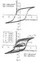
- Fig. 14 depicts the hysteresis loop of such a PGO thin film, which is square, symmetrical and well saturated, at an applied voltage of 5 V.
- the 2Pr is 3.98 ⁇ C/cm 2
- the 2Ec is 128 KV/cm.
- Fig. 15 depicts the hysteresis loops of the PGO thin films at IV, trace 68, 2V, trace 70, 3V, trace 72, 4V, trace 74, and 5V, trace 76.
- the hysteresis loops of the PGO thin film were nearly saturated above 3V.
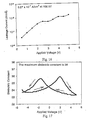
- Fig. 16 depicts the I-V curve of a 300-nm thick MOCVD PGO film. Excellent I-V characteristics were observed.
- the leakage current density of the Pb 5 Ge 3 O 11 thin film increased with increasing applied voltage, and is about 5.07x10 -7 A/cm 2 at 100 KV/cm.
- the dielectric constant is another important issue for memory devices, especially in one-transistor memory applications.
- the dielectric constant of Pb 5 Ge 3 O 11 thin films shows behavior similar to most ferroelectric materials, that is, the dielectric constant changes with applied voltage.
- the maximum dielectric constant of the Pb 5 Ge 3 O 11 thin film is about 36, as shown in Fig. 17.
- the BST films were prepared on Pt/Ti/SiO 2 /Si substrates by MOCVD. Typical process conditions are as shown in Table 2. Bis(2,2,6,6-tetramethyl-3, 5-heptanedionate)strontium hydrate [Sr(TMHD) 2 ], Bis(2,2,6,6-tetramethyl-3, 5-heptanedionate)barium hydrate [Ba(TMHD) 2 ], and Titanium i -propoxide [Ti(OPr)4] (TIP) were used as starting materials.
- the Ba(TMHD) 2 , Sr(TMHD) 2 and TIP were dissolved in a solution of tetrahydrofuran, 2-ethyl-1-hexanol, and tetraglyme with the molar ratio 6-9:1-3:1, a variation of solvent I, to form a source solution with a concentration of 0.1 M - 0.3 M.
- the source solution was pumped into a heated vaporizer at 220°C - 250°C at a rate of 0.2 ml/min - 0.6 ml/min.
- the mixed precursor vapors were carried into the reactor with preheated nitrogen at 220°C - 250°C. After deposition, the BST films were cooled to room 'temperature in an oxygen atmosphere. Smooth and specular BST films were obtained.
- the composition of the BST thin films was analyzed by using energy dispersion X-ray analysis (EDX) and Rutherford back scattering (RBS). The BST thickness and thickness uniformity were measured by a UV/VIS spectrometer. The phases of the films were identified using X-ray diffraction (XRD).
- the surface morphologies and surface roughness of BST films on Pt/Ti/SiO 2 /Si substrates were measured by Atomic Force Microscopy (AFM).
- the optical properties of the BST films on Pt/Ti/SiO 2 /Si substrates were measured by both UV-VIS-NIR. spectrophotometry, and variable angle spectroscopic ellipsometry.
- the ferroelectric properties were measured using a standardized RT66A tester.
- the top electrodes were sputtered platinum using a shadow mask. The area of the top electrode was 2.1 ⁇ 10 -4 cm 2 . Leakage currents were measured using Keithley 617 programmable electrometer.
- the current was measured once by applying the field, such that the top electrode is the higher potential (Top-High) and then by reversing the field (Top-Low).
- the dielectric constant was measured as a function of frequency and also bias voltage, using a HP 4192A LF impedance analyzer.
- the films were deposited at temperatures ranging from 500°C to 750°C. As-deposited films were specular, crack-free, uniform, and adhered well to the substrates. These films showed very smooth surfaces as viewed by both optical microscopy and atomic force microscopy.
- the experimental results demonstrate that BST crystalline phase formation was initiated at 600°C - 650°C and was complete at a temperature of 700°C.
- the microstructure of the films was found to be dense and homogenous. Under AFM examination, the film's surface morphology appeared uniformly distributed, fine grained and crack-free. The average grain size was approximately 100 nm for films deposited at 700°C. The refractive index of the films was near 2.2, at a wavelength of 640 nm, measured by variable angle spectroscopic ellipsometry. This value is very close to that of bulk BST samples, which indicates formation of a highly dense film.
- the dielectric constant is a critical parameter.
- the frequency dependence of the dielectric constant exhibits a monotonic decrease with increasing frequency. From 200 kHz to 1000 kHz, the dielectric constant value tends to be stable at about 600.
- Low leakage current density is another important consideration for memory device applications. Excellent I-V characteristics were observed.
- the leakage current density at 100 kv/cm was approximately 2.0 ⁇ 10 -7 A/cm 2 . Under the same conditions of an applied electric field, the leakage current resulting from random polycrystalline BST thin films are similar to those from heteroepitaxial BST thin films.
- the SBT films were prepared on Pt/Ti/Si0 2 /Si substrates by MOCVD.
- the films were deposited at the desired temperature directly, or were deposited at low temperature for nucleation, and then post-annealed at a higher temperature for crystallization.
- the organic precursors were mixed and dissolved in the solvents to form a source solution with a concentration of 0.1 - 0.5 M/L of SBT.
- the source solution was injected at a rate of 0.1 ml/min - 0.5 ml/min by a liquid pump into the heated vaporization chamber at a temperature of about 220°C - 250°C, to form a precursor gas.
- the mixed precursor gases were brought into reactor chamber at temperature of 550 - 650°C using preheated nitrogen flow at 220 - 250°C.
- the oxygen was separately fed into the reactor chamber.
- the precursor gas went through a by-pass line for approximately three minutes before starting deposition. After deposition, the SBT films were cooled to room temperature in a oxygen atmosphere.
- the thickness of the SBT films was about 100 nm - 200 nm.
- the top electrodes were sputtered platinum using a shadow mask.
- the area of the top electrode was 2.1 x 10 -4 cm 2 . It was found that nucleation of SBT started at a deposition temperature close to 500°C and grain growth dominated at 700°C or above. With increasing deposition temperature, the grain size of SBT thin films increased from 100 nm 200 nm. High quality SBT thin films were obtained.
- the SBT thin films with grain size about 100 nm exhibit the following properties: thickness of about 16 nm - 190 nm; 2Pr of about 7.8 mC/cm 2 - 11.4 mC/cm 2 at 5V; EC of about 50 kv/cm - 65 kv/cm; leakage current of about 8.0 ⁇ 10 -9 A/cm 2 -9.5 ⁇ 10 -9 A/cm 2 at 150 kv/cm; dielectric constant of about 100 - 200; and fatigue rate of about 0.94 - 0.98 after 1O 9 cycles at 5 V.
Landscapes
- Chemical & Material Sciences (AREA)
- Inorganic Chemistry (AREA)
- General Chemical & Material Sciences (AREA)
- Chemical Kinetics & Catalysis (AREA)
- Engineering & Computer Science (AREA)
- Materials Engineering (AREA)
- Mechanical Engineering (AREA)
- Metallurgy (AREA)
- Organic Chemistry (AREA)
- Chemical Vapour Deposition (AREA)
- Formation Of Insulating Films (AREA)
- Semiconductor Memories (AREA)
Abstract
Description
- This invention relates to MOCVD precursor solutions in mixed solvents which find use in depositing ferroelectric and dielectric thin films, such as PbZrxTi1-xO3 (PZT), SrBi2Ta2O9 (SBT), Ba1-xSrxTiO3 (BST) and Pb5Ge3O11 (PGO).
- Liquid delivery MOCVD processes have been used for deposition of ferroelectric and dielectric thin films. Compared with solid source techniques, the advantages of using liquid source for MOCVD are well known and include achieving homogeneity at an atomic level in a solution, which leads to accurate control of the stoichiometry of the deposited films, which have, when using single source techniques, complex compositions. Because the chemical reactants for a liquid source may be purified conveniently by distillation and crystallization, films of high purity may be fabricated by liquid-delivery MOCVD processing. Another advantage of liquid source delivery is that liquid source materials are easy to transport from a source container to a vaporizer, and may be accurately infused into the reaction chamber using a liquid flow meter. Liquid source materials may be atomized to increase evaporation area, which will increase evaporation amount and promote the complete evaporation of the liquid source material. However, because liquid-delivery MOCVD techniques are relatively new commercial technologies, there are still many problems to be dealt with, including those related to surface roughness, surface morphologies and properties of ferroelectric and dielectric thin films deposited by the liquid-delivery MOCVD techniques. In liquid-delivery MOCVD processes, solvents are used to dissolve precursors, to transport the precursors from a source container to a vaporizer, and to promote atomization of the precursors, resulting in complete evaporation of the precursor.
- Because the solvents are introduced into a MOCVD reactor, and join in the precursor reactions and film depositions, the solvents have a significant effect on the film qualities, such as surface roughness, morphology and other properties. Selection of solvents is an important decision when using MOCVD techniques for ferroelectric and dielectric thin film deposition. In spite of the importance of solvent selection, most known research has been directed towards selection of precursors, with only a minor amount of research being directed towards solvents selection for MOCVD processes.
- The challenge of preparing PZT ferroelectric metal oxide thin films via MOCVD methods are described in G.-R. Bai, A. Wang, I.-F. Tsu, C. M. Foster, and 0. Auciello, Integrated Ferroelectrics, Vol. 21, 291(1998); M. Shimizu, H. Fujisawa and T. Shiosaki, Integrated Ferroelectrics, Vol. 14, 69(1997); and U.S. Patent No. 5,453,494 to Kirlin et al., for Metal complex source reagents for MOCVD, granted September 26, 1995.
- U.S. Patent No. 5,820,664 to Gardiner et al., for Precursor compositions for chemical vapor deposition, and ligand exchange resistant metal-organic precursor solutions comprising same, granted October 13, 1998, describes the difficulties in this area related to the various precursors which must be used.
- Currently, Pb(TMHD)2 is an accepted lead precursor, however, its low volatility and poor stability renders its application in MOCVD difficult, as described in I.-S. Chen, J. F. Roeder, T. E. Glassman, and T. H. Baum, Chem. Mater., 11 No. 2, 209 (1999). With the introduction of a liquid-delivery system, the delivery of precursors is greatly improved, but there are still many problems, as described in J. F. Roeder, B. A. Vaartstra, P. C. Van Buskirk, and H. R. Beratan, Mater. Res. Soc. Symp. Proc. 415, 123 (1996).
- The key problems are the precursor's stability and volatility, the solution reactions in PZT precursor solutions, the precursor's solubility, the precursor's decomposition tendency in the heated delivery line, the purity of the precursor solutions, and the block of the delivery line and the vaporizer. To solve these problems, the use of different precursors is necessary. The existing precursor solution is the combination of tetrahydrofunan (THF) and tetraglyme and iso-propanol, in which the solid ferroelectric precursors are dissolved.
- In accordance with the invention, there is now provided a ferroelectric and dielectric source solution for use in chemical vapor deposition, the solution including ferroelectric and dielectric chemical vapor deposition precursors, and a solvent for carrying the ferroelectric/dielectric chemical vapor deposition precursors taken from the group of solvents consisting essentially of type A solvents, including tetraglyme, triglyme, triethylenetetramine, N,N,N',N'-tetramethylethylenediamine; N,N,N',N',N",N"-pentamethyldiethylenetriamine; and 2,2'-bipyridine; type B solvents including tetrahydrofuran, butyl ethyl ether, tert-butyl ethyl ether, butyl ether, and pentyl ether; and type C solvents including iso-propanol, 2-butanol, 2-ethyl-1-hexanol, 2-pentanol, toluene, xylene and butyl acetate; and mixtures of solvent types A, B and C.
- Such a solution permits optimum liquid-delivery MOCVD processes for ferroelectric and dielectric thin film deposition, enables the achievement of improved surface roughness, surface morphology and ferroelectric/dielectric properties of the deposited film and provides a precursor in a form which is stable, i.e., does not precipitate, when stored for an extended period of time.
- The invention is described below in greater detail by way of example only with reference to the accompanying drawings, in which
- Fig. 1 depicts the surface roughness of PZT thin films using mixed solvents;
- Fig. 2 depicts X-ray patterns of PZT thin films on Pt/Ir electrodes using mixed solvents;
- Fig. 3 depicts the microstructures of PZT thin films on Pt/Ir electrodes using mixed solvents;
- Fig. 4a,b are the hysteresis loops of PZT thin film on Pt/Ir electrodes using solvent I ;
- Fig. 5a,b are the hysteresis loops of PZT thin film on Pt/Ir electrodes using solvent II ;
- Fig. 6a,b are the hysteresis loops of PZT thin film on Pt/Ir electrodes using solvent III ;
- Fig. 7 depicts the obtained polarization and coercive field values of PZT thin films on Pt/Ir electrodes using mixed solvents ;
- Fig. 8 depicts the leakage currents of PZT on Pt/Ir electrodes using mixed solvents ;
- Fig. 9 depicts a hysteresis loop of a PZT thin film, formed using solvent IV, measured under 5V applied voltage ;
- Fig. 10 depicts the X-ray patterns of PGO thin films obtained by the method of the invention ;
- Fig. 11 depicts the composition of PGO thin films;
- Fig. 12 depicts the X-ray pattern of PGO thin films made with multiple MOCVD and annealing;
- Fig. 13 depicts the microstructure of c-axis oriented PGO thin films made using multiple MOCVD and annealing ;
- Fig. 14 depicts the hysteresis loop of a PGO thin film at 5V ;
- Fig. 15 depicts the hysteresis loop of a PGO thin film at various voltages ;
- Fig. 16 depicts the leakage current of a PGO thin film ; and
- Fig. 17 depicts the dielectric constant of a PGO thin film.
-
- The invention provides the means which permits smoothing the surface roughness, surface morphology and properties of ferroelectric and dielectric, such as oxide, thin films using mixed solvents. In liquid-delivery metal organic chemical vapor deposition (MOCVD) systems, solvents are used to dissolve precursors, transport the precursors from a source container to a vaporizer, to assist in the atomization of precursors and make them complete evaporation. The solvents are also introduced into a MOCVD reactor and join the precursor reactions and film depositions.
- In general, a solvent should have following properties: high solubility power; no interaction between precursor and solvent when they are mixed, i.e., long term stability; they should not participate in a reaction, other than to provide a dilution effect; they should have an appropriate boiling point, close to the vaporization temperature of the precursors; they should have low viscosity; and they should be inexpensive.
- The solvents which may be used during deposition of typical thin films are listed in Table 1. The precursors are listed in Table 2.
Solvent Properties and Classification Organic Stabilizer Boiling Point (°C) Formula Type A Solvent: strong coordinated to the metal center, stabilize the metal organic precursors in their gas phases. Tetraglyme 275 CH3(OCH2CH2)4OCH3 Triglyme 216 CH3(OCH2CH2)3OCH3 Triethylenetetramine 266 H2N(CH2CH2NH)2CH2CH2NH2 N,N,N',N'- tetramethylethylenediamine 121 (CH3)2NCH2CH2N(CH3)2 N,N,N',N',N",N"- pentamethyldiethylenetriamine 198 [(CH3)2NCH2CH2]2NCH3 2,2'-bipyridine 273 (NC5H4)2 Type B Solvent: dissolves metal organic precursors to give liquid precursors which can be applied in liquid-delivery system for MOCVD metal oxide thin film deposition Tetrahydrofuran 65-67 C4H8O Butyl ethyl ether 92 CH3(CH2)3OC2H5 tert-butyl ethyl ether 73 (CH3)3COC2H5 Butyl ether 142-143 [CH3(CH2)3]O Pentyl ether 187 [CH3(CH2)4]O Type C Solvent: alcohols for liquid precursor property adjustment iso-propanol 97 (CH3)2CHOH 2-butanol 98 C2H5CH(OH)CH3 2-ethyl-1-hexanol 183-186 CH3(CH2)3CH(C2H5)CH2OH 2-pentanol 118 CH3CH2CH2CH(OH)CH3 Toluene 111 C6H5CH3 Xylene 137-144 C6H4(CH3)2 Butyl Acetate 124-126 C6H1202 The properties of precursors for ferroelectric and dielectric (oxide) thin films Precursor Formula Appearance at Room Temperature Moisture stability Vapor Pressure (mm Hg) Decompos ition Temp (°C) Ba(TMHD)2 Ba(C11H19O2)2 white powder sensitive 225°C/0.05 285°C Bi Triphenyl Bi(C6H5)3 white crystal stable 100°C/0.2 310°C Ge(OEt)4 Ge(OC2H5)4 colorless liquid sensitive 185°C La(TMHD)3 La(C11H19O2)3 white powder 210°C/0.2 370°C Nb(OEt)5 Nb(OC2H5)5 yellow liquid sensitive 145°C/0.1 350°C Pb Tetraphenyl Pb(C6H5)4 white powder 230°C/0.05 325°C Pb(TMHD)2 Pb(C11H19O2)2 white powder 180°C/0.05 325°C Sr(TMHD)2 Sr(C11H19O2)2 light yellow powder stable 230°C/0.05 250°C Ta(OEt)4 Ta(OC2H5)5 yellow liquid sensitive 145°C/0.1 350°C Ti(OEt)4 Ti(OC2H5)4 colorless crystal sensitive 138°C/5 Ti(POr')4 Ti(OC3H7)4 colorless liquid sensitive 58°C/1 Zr(TMHD)4 Zr(C11H19O2)4 white crystal 180°C/0.1 Zr(OBu')4 Z(OC4H9)4 yellow liquid sensitive 90°C/5 - Liquid solvents for metal organic precursor may be obtained using combinations of the three different organic solvent types, selected from each type A, type B and type C, respectively. From Tables 1 and 2, it may be seen that most solvents have boiling points which are lower than the vaporization temperature of the precursors to be dissolved in the solvents; therefore, in order to obtain appropriate boiling points, mixtures of various solvents must be used. This invention describes the use of mixed solvents. Exemplary compositions of the kinds of solvents are as follows:
- Solvent I: Molar ratio of tetrahydrofuran, iso-propanol and tetraglyme of about 6-10:1-4:1, preferably of about 8:2:1.
- Solvent II: Molar ratio of butyl ether, iso-propanol and tetraglyme of about 6-10:1-4:1, preferably of about 8:2:1.
- Solvent III: Molar ratio of butyl ether, tetrahydrofuran, iso-propanol and tetraglyme of about 3-5:3-5:1-4:1, preferably of about 4:4:2:1.
- Solvent IV: Molar ratio of butyl ether and tetraglyme: 8:1.
-
- The general solvent composition is a mixture of a solvent of type B, type C and type A in a molar ration of about 6-10:1-4:1, and preferably about 8:2:1; or a mixture of a solvent of type B and type A in a molar ration of about 6-10:1-3, and preferably about 8:1.
- An Emcore oxide MOCVD reactor, having a liquid-delivery system, is used for the growth of PZT thin films. The precursors for ferroelectric and dielectric thin films are as listed in Table 2. Pb(TMHD)2, Zr(TMHD)4 and Ti(OPr i )4, where THMD is 2,2,6,6-tetramethyl-3,5-heptanedionate and OPr' is iso-protoxide, in a molar ratio of about 1.2 : 0.5 : 0.5 are dissolved into mixed solvents I-III. The precursor solutions have a concentration of 0.1 M/L of PZT. The solution is injected into a vaporizer at a temperature of about 200°C - 250°C and a pump at a rate of 0.1 - 0.5 ml/min, to form precursor gases. The precursor gases are brought into the MOCVD reactor using a preheated argon flow at 200°C - 250°C. The deposition temperatures and pressure are 500°C - 650°C and 10 Torr, respectively. The shroud flow; Ar at 4000 sccm, with oxygen at 1000 - 2500 sccm, is fed into the reactor. After deposition, the PZT thin films are cooled to room temperature in a oxygen atmosphere. In order to improve the ferroelectric properties of PZT thin films, the as-deposited PZT thin films may be annealed at 600°C - 700°C, in an oxygen atmosphere before and after top electrode deposition.
- Fig.1 depicts the surface roughness of PZT thin films at various deposition temperatures using the mixed solvents I-III, generally at 10, Using solvent I, trace 12, lower surface roughness was found at lower deposition temperature, while the surface roughness increased as deposition temperatures increased. Solvent II, trace 14, produced a PZT layer wherein the surface roughness was higher at lower deposition temperature, and smoothed as deposition temperatures increased. Solvent III,
trace 16, is a mixed solvent of solvent I and solvent II. As shown in Fig. 1, the surface roughness may be controlled by using solvent III, and adjusting the ratio of solvent I : solvent II. Therefore, the surface roughness of ferroelectric and dielectric thin films deposited at different temperatures may be improved by selection and mixing of various solvents. - Fig. 2 depicts X-ray patterns of PZT thin films on Pt/Ir electrodes using mixed solvents, wherein trace 18 is obtained using solvent I, trace 20 is obtained using solvent II, and trace 22 is obtained using solvent III. The preferred orientation of PZT thin films may be adjusted using various mixtures of solvents. The X-ray patterns show that the (100) orientation of PZT thin films tend to be strongest using solvent III, as trace 22 has a broader 2-theta value for the 100 orientation.
- Fig. 3 depicts the microstructures of PZT thin films on Pt/Ir electrodes using mixed solvents I-III. The surface morphologies may also be changed using various mixed solvents of the invention. Smaller grains are found in PZT thin films deposited using solvents I and III. Dense PZT thin films, with large plate shape grains, are obtained using solvent II, which thin film subsequently demonstrated excellent ferroelectric properties.
- Figs 4-6 depict the hysteresis loops of PZT thin films deposited by various solvents. The PZT thin films made using all of the solvents identified herein have very good ferroelectric properties. Fig. 4 depicts the hysteresis loops of PZT thin film on Pt/Ir electrodes using solvent I; Fig. 5 depicts the hysteresis loops of PZT thin film on Pt/Ir electrodes using solvent II; and Fig. 6 depicts the hysteresis loops of PZT thin film on Pt/Ir electrodes using solvent III
- Fig. 4a depicts the hysteresis loop at 5V for a PZT film deposited using solvent I, with annealing before and after top electrode deposition (TE), at 24. The obtained polarization (2Pr) is 43.3µC/cm2, and the coercive field (2Ec) is 107 kv/cm. Fig. 4b depicts the hysteresis loop for the PZT layer with annealing before and after TE, at various applied voltages, wherein trace 26 is the loop for IV,
trace 28 is the loop for 2V,trace 30 is the loop for 3V,trace 32 is the loop for 4V, and trace 34 is the loop for 5V. - Fig. 5a depicts the hysteresis loop for a PZT film deposited using solvent II, with annealing before and after TE, at 36. The 2Pr is 39.8 µC/cm2, and the 2Ec is 73.2 kv/cm. Fig. 5b depicts the hysteresis loop for the PZT layer with annealing before and after TE, at various applied voltages, wherein
trace 38 is the loop for 1V,trace 40 is the loop for 2V,trace 42 is the loop for 3V, trace 44 is the loop for 4V, and trace 46 is the loop for 5V. - Fig. 6a depicts the hysteresis loop for a PZT film deposited using solvent III, with annealing before and after TE, at 48. The 2Pr is 42.1 µC/cm2, and the 2Ec is 105 kv/cm. Fig. 6b depicts the hysteresis loop for the PZT layer with annealing before and after TE, at various applied voltages, wherein
trace 50 is the loop for 1V,trace 52 is the loop for 2V; trace 54 is the loop for 3V,trace 56 is the loop for 4V, and trace 58 is the loop for 5V. - Compared with solvent I and III, the best ferroelectric properties are found in the PZT thin film deposited using solvent II. The hysteresis loops with 2Pr value of 39.8 µC/cm2 and 2Ec value of 73.2 kv/cm were square and symmetric and almost saturated from a 2V applied voltage.
- Fig. 7 depicts the 2Pr,
trace 60, and 2Ec,trace 62, values of PZT thin films on Pt/Ir electrodes using solvents I, II and III. The PZT thin films made by solvent II had the smallest coercive field, 73 kv/cm, and also smallest leakage current, as shown in Fig. 8, which depicts theleakage currents 64 of PZT thin films made using solvents I, II and III. - Although the previously described solvent and precursor combinations provide a PZT film having good ferroelectric characteristics, to be commercially viable, the precursor/solvent combination must have a reasonable shelf life to facilitate manufacture, mixing, transportation and storage prior to use in a MOCVD process. As previously noted, an object of the invention is to provide a stable metal β-diketone precursor. Butyl ether may be used for this purpose. The solid precursors used are Pb(TMHD)2, Zr(OPr')4H(OPr'), Zr(TMHD)2, Ti(OPr')4 or Ti(OPr')2(TMHD)2, where OPr' is iso-propoxide (OCH(CH3)2), and Ge(OEt)4, where OEt is ethoxide (OC2H5), for the preparation of ferroelectric precursors for PZT and PGO ferroelectric and dielectric thin film deposition via MOCVD. The solid precursors are stoichiometrically mixed and dissolved in a mixture of butyl ether and tetraglyme organic solution, solvent IV. This precursor solution may be used as MOCVD source for the ferroelectric and dielectric thin films deposition.
- The precursor solution is stable at room temperature under inert atmosphere over a long time, which means the volatility of solid compounds does not degrade even when they are dissolved in this organic solution over a long time. The precursor solution of the invention did not block the vaporizer over a long time for the PZT thin film deposition, and gave the PZT thin film with good ferroelectric properties, as shown in the Fig. 9.
- In this example, the solid precursors, Pb(TMHD)2 [3.13 g], Zr(OPr')4H(OPr') [0.88 g] and Ti(OPr')4 [0.65 g], were used at a molar ratio of 1-1.2:0.3-0.7:0.2-0.7, and preferably at a molar ratio of 1.1:0.5:0.5, and dissolved in a mixture of butyl ether [36.36 g[ and tetraglyme [2.42 g], at a molar ratio of 8:1. All of the solid precursors are sublimed before solution preparation. The butyl ether and tetraglyme are used as received from Aldrich. A clear solution is obtained after all of the solid precursors dissolved. The precursor solution was kept in a closed glass bottle for more than one month. The organic solvents, butyl ether and tetraglyme, were then removed by dynamic vacuum at 100°C. The dried solid mixture precursor was heated to about 170°C, for sublimation. More than 95% of the dried solid mixture precursor was found to be volatile. This result indicates that the solid mixture precursor is stable in the organic solution mixture for over one month.
- A PZT thin film was formed using the precursor solution described in Example One, via MOCVD. The PZT precursor solution was delivered into the vaporizer at the flow rate of 0.1 ml/min - 0.5 ml/min, and the vaporizer temperature was set between 200°C - 250°C The reactor pressure was between about 5 Torr - 10 Torr, and the deposition temperature was between 550°C - 700°C. High quality PZT thin films were obtained. Fig. 9 depicts a
hysteresis loop 66 of the PZT thin film, which was measured under 5V applied voltage, and which achieved a 2Pr of 53.8 µC/cm2 and 2Ec of 87 kv/cm. - An oxide MOCVD reactor was used for the growth of c-axis oriented Pb5Ge3O11 thin films. Pb(TMHD) and Ge(OEt)4 with a molar ratio of 4-6:2-4, and preferably of about 5:3, were dissolved in a mixed solvent of butyl ether, iso-propanol and tetraglyme in the molar ratio of about 6-9:1-3:1, and preferably of about 8:2:1, solvent II. The precursor solutions had a concentration of 0.1 M/L of PGO. The solution was injected into a vaporizer at 140°C - 180°C by a pump at a rate of 0.1 ml/min. - 0.2 ml/min to form precursor gases. The growth line was 165°C - 245°C. The deposition temperatures and pressure were 300°C - 600°C and 5 Torr - 10 Torr, respectively. The shroud flow,
Ar 1000 sccm - 6000 sccm, with an oxygen partial pressure of 20% - 50%, was led into the reactor. Substrates of Si, SiO2, Pt/Ti/SiO2/Si, Pt-Ir alloy/Ti/SiO2/Si and Ir/Ti/SiO2/Si were used for growth of PGO thin films at various deposition times. After PGO film deposition, rapid thermal annealing (RTA) processes were used to improve the ferroelectric and electrical properties of the PGO thin films. - The experimental results show that c-axis PGO thin films had excellent ferroelectric properties. Fig. 10 depicts the X-ray patterns of Pb5Ge3O11 films deposited on Ir substrates from 400°C to 550°C. The nucleation of c-axis oriented PGO phase began at a deposition temperature below 400°C. As the substrate temperature increased, the grain growth and c-axis oriented PGO film occurred. The very sharp peaks, (001), (002), (003), (004), (005), and (006), were observed from PGO thin films at a substrate temperature of about 500°C, which indicated the formation of a well-crystallized Pb5Ge3O11 film having the preferred c-axis orientation. At temperatures in excess of 500°C, a small second phase Pb3GeO5 layer was formed, which increased as the substrate temperature increased. The intensity of the c- axis peaks decreased with increasing this phase of Pb3GeO5. From the composition analysis shown in Fig. 11, the Pb content increased and the Ge content decreased as the substrate temperature increased during MOCVD.
- The stoichiometrical Pb5Ge3O11 thin films were obtained at substrate temperature of about 500°C, which is consistent with X-ray analysis results, shown in Fig. 12. The PGO thin film has a high c-axis orientation of Pb5Ge3O11, with a little of the second phase Pb3GeO5. Fig. 13 depicts the microstructure of c-axis oriented PGO thin films using the multiple MOCVD arid annealing processes. The average grain size of the PGO film is about 0.8 mm. The layered structure confirmed that the c-axis oriented PGO thin films grew layer-by-layer along the c-axis direction. The thickness of PGO thin film was measured to be about 300 nm.
- PGO thin films made by MOCVD and annealing processes exhibited very good ferroelectric and electrical properties. Fig. 14 depicts the hysteresis loop of such a PGO thin film, which is square, symmetrical and well saturated, at an applied voltage of 5 V. The 2Pr is 3.98 µC/cm2, and the 2Ec is 128 KV/cm. Fig. 15 depicts the hysteresis loops of the PGO thin films at IV,
trace trace trace trace 74, and 5V, trace 76. The hysteresis loops of the PGO thin film were nearly saturated above 3V. - Low leakage current density is an important consideration for memory device applications. Fig. 16 depicts the I-V curve of a 300-nm thick MOCVD PGO film. Excellent I-V characteristics were observed. The leakage current density of the Pb5Ge3O11 thin film increased with increasing applied voltage, and is about 5.07x10⁻⁷ A/cm2 at 100 KV/cm.
- 'The dielectric constant is another important issue for memory devices, especially in one-transistor memory applications. The dielectric constant of Pb5Ge3O11 thin films shows behavior similar to most ferroelectric materials, that is, the dielectric constant changes with applied voltage. The maximum dielectric constant of the Pb5Ge3O11 thin film is about 36, as shown in Fig. 17.
- The BST films were prepared on Pt/Ti/SiO2/Si substrates by MOCVD. Typical process conditions are as shown in Table 2. Bis(2,2,6,6-tetramethyl-3, 5-heptanedionate)strontium hydrate [Sr(TMHD)2], Bis(2,2,6,6-tetramethyl-3, 5-heptanedionate)barium hydrate [Ba(TMHD)2], and Titanium i-propoxide [Ti(OPr)4] (TIP) were used as starting materials. For the liquid-delivery system, the Ba(TMHD)2, Sr(TMHD)2 and TIP were dissolved in a solution of tetrahydrofuran, 2-ethyl-1-hexanol, and tetraglyme with the molar ratio 6-9:1-3:1, a variation of solvent I, to form a source solution with a concentration of 0.1 M - 0.3 M. The source solution was pumped into a heated vaporizer at 220°C - 250°C at a rate of 0.2 ml/min - 0.6 ml/min.
- The mixed precursor vapors were carried into the reactor with preheated nitrogen at 220°C - 250°C. After deposition, the BST films were cooled to room 'temperature in an oxygen atmosphere. Smooth and specular BST films were obtained. The composition of the BST thin films was analyzed by using energy dispersion X-ray analysis (EDX) and Rutherford back scattering (RBS). The BST thickness and thickness uniformity were measured by a UV/VIS spectrometer. The phases of the films were identified using X-ray diffraction (XRD).
- The surface morphologies and surface roughness of BST films on Pt/Ti/SiO2/Si substrates were measured by Atomic Force Microscopy (AFM). The optical properties of the BST films on Pt/Ti/SiO2/Si substrates were measured by both UV-VIS-NIR. spectrophotometry, and variable angle spectroscopic ellipsometry. The ferroelectric properties were measured using a standardized RT66A tester. The top electrodes were sputtered platinum using a shadow mask. The area of the top electrode was 2.1·10-4cm2. Leakage currents were measured using Keithley 617 programmable electrometer. At each stage, the current was measured once by applying the field, such that the top electrode is the higher potential (Top-High) and then by reversing the field (Top-Low). The dielectric constant was measured as a function of frequency and also bias voltage, using a HP 4192A LF impedance analyzer.
- The films were deposited at temperatures ranging from 500°C to 750°C. As-deposited films were specular, crack-free, uniform, and adhered well to the substrates. These films showed very smooth surfaces as viewed by both optical microscopy and atomic force microscopy. The experimental results demonstrate that BST crystalline phase formation was initiated at 600°C - 650°C and was complete at a temperature of 700°C. The XRD patterns of the as-deposited BST films on Pt/Ti/SiO2/Si substrates at 700°C were measured. The major XRD peaks corresponding to (100), (200), (110), (210), (211) planes, were observed and demonstrate that the single BST phase is formed. The microstructure of the films was found to be dense and homogenous. Under AFM examination, the film's surface morphology appeared uniformly distributed, fine grained and crack-free. The average grain size was approximately 100 nm for films deposited at 700°C. The refractive index of the films was near 2.2, at a wavelength of 640 nm, measured by variable angle spectroscopic ellipsometry. This value is very close to that of bulk BST samples, which indicates formation of a highly dense film.
- For high density DRAM application, the dielectric constant is a critical parameter. The frequency dependence of the dielectric constant exhibits a monotonic decrease with increasing frequency. From 200 kHz to 1000 kHz, the dielectric constant value tends to be stable at about 600. Low leakage current density is another important consideration for memory device applications. Excellent I-V characteristics were observed. The leakage current density at 100 kv/cm was approximately 2.0·10-7 A/cm2. Under the same conditions of an applied electric field, the leakage current resulting from random polycrystalline BST thin films are similar to those from heteroepitaxial BST thin films.
- The SBT films were prepared on Pt/Ti/Si02/Si substrates by MOCVD. The films were deposited at the desired temperature directly, or were deposited at low temperature for nucleation, and then post-annealed at a higher temperature for crystallization. For SBT thin films, Bis(2,2,6,6-tetramethyl-3, 5- heptanedionate) strontium hydrate [Sr(TMHD)2], triphenylbismuth [Bi(C6H5)3], tantalum ethoxide [Ta(OC2H5)5] were used as starting materials with mixture of molar ratio of tetrahydrofuran (6 - 10), toluene, xylene, butyl acetate or iso-propanol (1 - 4) and tetraglyme (1 - 2), as the solvents. The organic precursors were mixed and dissolved in the solvents to form a source solution with a concentration of 0.1 - 0.5 M/L of SBT. The source solution was injected at a rate of 0.1 ml/min - 0.5 ml/min by a liquid pump into the heated vaporization chamber at a temperature of about 220°C - 250°C, to form a precursor gas. The mixed precursor gases were brought into reactor chamber at temperature of 550 - 650°C using preheated nitrogen flow at 220 - 250°C. The oxygen was separately fed into the reactor chamber. The precursor gas went through a by-pass line for approximately three minutes before starting deposition. After deposition, the SBT films were cooled to room temperature in a oxygen atmosphere. The thickness of the SBT films was about 100 nm - 200 nm. The top electrodes were sputtered platinum using a shadow mask. The area of the top electrode was 2.1 x 10⁻⁴ cm2. It was found that nucleation of SBT started at a deposition temperature close to 500°C and grain growth dominated at 700°C or above. With increasing deposition temperature, the grain size of SBT thin films increased from 100
nm 200 nm. High quality SBT thin films were obtained. - The SBT thin films with grain size about 100 nm exhibit the following properties: thickness of about 16 nm - 190 nm; 2Pr of about 7.8 mC/cm2 - 11.4 mC/cm2 at 5V; EC of about 50 kv/cm - 65 kv/cm; leakage current of about 8.0 ·10-9 A/cm2-9.5·10-9 A/cm2 at 150 kv/cm; dielectric constant of about 100 - 200; and fatigue rate of about 0.94 - 0.98 after 1O9 cycles at 5 V.
Claims (11)
- A source solution for use in chemical vapor deposition, the solution comprising:a chemical vapor deposition precursor; anda solvent for the chemical vapor deposition precursor selected from type A solvents including tetraglyme, triglyme, triethylenetetramine, N,N,N',N'-tetramethylethylenediamine, N,N,N',N',N",N"-pentamethyldiethylenetriamine, and 2,2'-bipyridine; type B solvents including tetrahydrofuran, butyl ethyl ether, tert-butyl ethyl ether, butyl ether and pentyl ether; type C solvents including iso-propanol, 2-butanol, 2-ethyl-1-hexanol, 2-pentanol, toluene, xylene and butyl acetate; and mixtures of types A, B and C solvents.
- A solution according to claim 1, wherein the solvent is a mixture of types A, B and C solvents in molar ratios of 1:6-10:1-4.
- A solution according to claim 2, wherein the molar ratios are about 1:8:2.
- A solution according to any one of claims 1 to 3, wherein the type A solvent is tetraglyme, the type B solvent is tetrahydrofuran and/or butyl ether and the type C solvent is isopropanol.
- A solution according to claim 1, wherein the solvent is a mixture of types A and B solvents in a molar ratio of 1-3:6-10.
- A solution according to claim 5, wherein the molar ratio is about 1:8.
- A solution according to any one of claims 1, 5 and 6, wherein the type A solvent is tetraglyme and the type B solvent is butyl ether.
- A solution according to any one of claims 1 to 7, wherein the chemical vapor deposition precursor is selected from Pb(TMHD)2, Zr(TMHD)4, Ti(OPr')4, Sr(TMHD)2, Bi(C6H5)3, Ta(OC2H5)5, Ba(TMHD)2 and Ge(OEt)4.
- A solution according to claim 8, wherein the chemical vapor deposition precursor is a combination of Pb(TMHD)2, Zr(TMHD)4 and (Ti(OPr')4 in molar ratios of about 1.2:0.5:0.5.
- A solution according to claim 8, wherein the chemical vapor deposition precursor is a combination of Pb(TMHD)2 and Ge(OEt)4 in a molar ratio of about 5:3.
- A solution according to any one of claims 1 to 10, wherein the chemical vapor deposition precursor has a concentration of about 0.1 m/ℓ in the solvent.
Applications Claiming Priority (2)
| Application Number | Priority Date | Filing Date | Title |
|---|---|---|---|
| US649381 | 1976-01-15 | ||
| US09/649,381 US6503314B1 (en) | 2000-08-28 | 2000-08-28 | MOCVD ferroelectric and dielectric thin films depositions using mixed solvents |
Publications (2)
| Publication Number | Publication Date |
|---|---|
| EP1184485A1 true EP1184485A1 (en) | 2002-03-06 |
| EP1184485B1 EP1184485B1 (en) | 2008-08-06 |
Family
ID=24604536
Family Applications (1)
| Application Number | Title | Priority Date | Filing Date |
|---|---|---|---|
| EP01307249A Expired - Lifetime EP1184485B1 (en) | 2000-08-28 | 2001-08-24 | MOCVD precursors in mixed solvents |
Country Status (6)
| Country | Link |
|---|---|
| US (1) | US6503314B1 (en) |
| EP (1) | EP1184485B1 (en) |
| JP (1) | JP4007573B2 (en) |
| KR (1) | KR100441549B1 (en) |
| DE (1) | DE60135191D1 (en) |
| TW (1) | TWI257435B (en) |
Cited By (3)
| Publication number | Priority date | Publication date | Assignee | Title |
|---|---|---|---|---|
| EP1433874A3 (en) * | 2002-12-20 | 2004-08-11 | Sharp Kabushiki Kaisha | Method for metal oxide thin film deposition via MOCVD |
| US7722926B2 (en) | 2005-08-02 | 2010-05-25 | Samsung Electronics Co., Ltd. | Organometallic compounds and methods of forming thin films including the use of the same |
| US7771913B2 (en) | 2006-04-04 | 2010-08-10 | Shin-Etsu Chemical Co., Ltd. | Resist composition and patterning process using the same |
Families Citing this family (8)
| Publication number | Priority date | Publication date | Assignee | Title |
|---|---|---|---|---|
| US6664116B2 (en) * | 2001-12-12 | 2003-12-16 | Sharp Laboratories Of America, Inc. | Seed layer processes for MOCVD of ferroelectric thin films on high-k gate oxides |
| JP4643196B2 (en) * | 2003-07-25 | 2011-03-02 | 三星電子株式会社 | Deposition method of metal compound film |
| KR101001741B1 (en) * | 2003-08-18 | 2010-12-15 | 삼성전자주식회사 | A capacitor of a semiconductor device, a method of manufacturing the same, and a memory device having a capacitor |
| US7157111B2 (en) * | 2003-09-30 | 2007-01-02 | Sharp Laboratories Of America, Inc. | MOCVD selective deposition of C-axis oriented PB5GE3O11 thin films on In2O3 oxides |
| KR20070026658A (en) * | 2004-06-10 | 2007-03-08 | 미츠비시 마테리알 가부시키가이샤 | Solution raw material for organometallic chemical vapor deposition and composite oxide-based dielectric thin film manufactured using the raw material |
| JP5514437B2 (en) * | 2007-12-28 | 2014-06-04 | 三菱マテリアル株式会社 | A method for manufacturing a dielectric thin film. |
| JP6225544B2 (en) * | 2013-07-31 | 2017-11-08 | 株式会社デンソー | Method for manufacturing piezoelectric element |
| EP3759550A1 (en) * | 2018-03-02 | 2021-01-06 | ASML Netherlands B.V. | Method and apparatus for forming a patterned layer of material |
Citations (1)
| Publication number | Priority date | Publication date | Assignee | Title |
|---|---|---|---|---|
| US5820664A (en) * | 1990-07-06 | 1998-10-13 | Advanced Technology Materials, Inc. | Precursor compositions for chemical vapor deposition, and ligand exchange resistant metal-organic precursor solutions comprising same |
Family Cites Families (7)
| Publication number | Priority date | Publication date | Assignee | Title |
|---|---|---|---|---|
| US5453494A (en) | 1990-07-06 | 1995-09-26 | Advanced Technology Materials, Inc. | Metal complex source reagents for MOCVD |
| US5225561A (en) | 1990-07-06 | 1993-07-06 | Advanced Technology Materials, Inc. | Source reagent compounds for MOCVD of refractory films containing group IIA elements |
| US5783716A (en) * | 1996-06-28 | 1998-07-21 | Advanced Technology Materials, Inc. | Platinum source compositions for chemical vapor deposition of platinum |
| US6010744A (en) * | 1997-12-23 | 2000-01-04 | Advanced Technology Materials, Inc. | Method for nucleation controlled chemical vapor deposition of metal oxide ferroelectric thin films |
| US6410343B1 (en) * | 1999-04-28 | 2002-06-25 | Sharp Laboratories Of America, Inc. | C-axis oriented lead germanate film and deposition method |
| US6590243B2 (en) * | 1999-04-28 | 2003-07-08 | Sharp Laboratories Of America, Inc. | Ferroelastic lead germanate thin film and deposition method |
| US6190925B1 (en) * | 1999-04-28 | 2001-02-20 | Sharp Laboratories Of America, Inc. | Epitaxially grown lead germanate film and deposition method |
-
2000
- 2000-08-28 US US09/649,381 patent/US6503314B1/en not_active Expired - Fee Related
-
2001
- 2001-07-24 JP JP2001223659A patent/JP4007573B2/en not_active Expired - Fee Related
- 2001-08-22 KR KR10-2001-0050722A patent/KR100441549B1/en not_active Expired - Fee Related
- 2001-08-24 TW TW090120891A patent/TWI257435B/en not_active IP Right Cessation
- 2001-08-24 EP EP01307249A patent/EP1184485B1/en not_active Expired - Lifetime
- 2001-08-24 DE DE60135191T patent/DE60135191D1/en not_active Expired - Lifetime
Patent Citations (1)
| Publication number | Priority date | Publication date | Assignee | Title |
|---|---|---|---|---|
| US5820664A (en) * | 1990-07-06 | 1998-10-13 | Advanced Technology Materials, Inc. | Precursor compositions for chemical vapor deposition, and ligand exchange resistant metal-organic precursor solutions comprising same |
Non-Patent Citations (3)
| Title |
|---|
| LI T K ET AL: "MFMOS CAPACITOR WITH PB5GE3O11 THIN FILM FOR ONE TRANSISTOR FERROELECTRIC MEMORY APPLICATIONS", MATERIALS RESEARCH SOCIETY SYMPOSIUM PROCEEDINGS, MATERIALS RESEARCH SOCIETY, PITTSBURG, PA, US, vol. 596, 29 November 1999 (1999-11-29), pages 443 - 448, XP001001349, ISSN: 0272-9172 * |
| LI TINGKAI ET AL: "Microstructure, phase and ferroelectric properties of PZT thin films on oriented multilayer electrodes", FERROELECTRIC THIN FILMS VIII;BOSTON, MA, USA NOV 29-DEC 2 1999, vol. 596, 29 November 1999 (1999-11-29), Mater Res Soc Symp Proc;Materials Research Society Symposium - Proceedings 2000 Materials Research Society, Warrendale, PA, USA, pages 199 - 204, XP001035017 * |
| ZHUANG W ET AL: "STUDIES ON PZT PRECURSOR SOLUTIONS", INTEGRATED FERROELECTRICS, NEW YORK, NY, US, vol. 26, no. 1, 7 March 1998 (1998-03-07), pages 277 - 284, XP000997100, ISSN: 1058-4587 * |
Cited By (3)
| Publication number | Priority date | Publication date | Assignee | Title |
|---|---|---|---|---|
| EP1433874A3 (en) * | 2002-12-20 | 2004-08-11 | Sharp Kabushiki Kaisha | Method for metal oxide thin film deposition via MOCVD |
| US7722926B2 (en) | 2005-08-02 | 2010-05-25 | Samsung Electronics Co., Ltd. | Organometallic compounds and methods of forming thin films including the use of the same |
| US7771913B2 (en) | 2006-04-04 | 2010-08-10 | Shin-Etsu Chemical Co., Ltd. | Resist composition and patterning process using the same |
Also Published As
| Publication number | Publication date |
|---|---|
| EP1184485B1 (en) | 2008-08-06 |
| JP4007573B2 (en) | 2007-11-14 |
| DE60135191D1 (en) | 2008-09-18 |
| TWI257435B (en) | 2006-07-01 |
| KR100441549B1 (en) | 2004-07-23 |
| JP2002121675A (en) | 2002-04-26 |
| US6503314B1 (en) | 2003-01-07 |
| KR20020017984A (en) | 2002-03-07 |
Similar Documents
| Publication | Publication Date | Title |
|---|---|---|
| EP0990059B1 (en) | Low temperature chemical vapor deposition process for forming bismuth-containing ceramic thin films useful in ferroelectric memory devices | |
| US6277436B1 (en) | Liquid delivery MOCVD process for deposition of high frequency dielectric materials | |
| EP0630424B1 (en) | Ferroelectric thin films made by metalorganic chemical vapor deposition | |
| US6110531A (en) | Method and apparatus for preparing integrated circuit thin films by chemical vapor deposition | |
| EP0792383B1 (en) | Tantalum and niobium reagents useful in chemical vapor deposition processes, and process for depositing coatings using the same | |
| US6511718B1 (en) | Method and apparatus for fabrication of thin films by chemical vapor deposition | |
| EP0807965B1 (en) | Method of manufacturing layered ferroelectric Bi containing film | |
| EP1184485B1 (en) | MOCVD precursors in mixed solvents | |
| Zhu et al. | SrBi2Ta2O9 thin films made by liquid source metal-organic chemical vapor deposition | |
| US6500489B1 (en) | Low temperature CVD processes for preparing ferroelectric films using Bi alcoxides | |
| US6274195B1 (en) | Organometallic complex process for the preparation thereof and metal organic chemical vapor deposition using same | |
| US6348705B1 (en) | Low temperature process for high density thin film integrated capacitors and amorphously frustrated ferroelectric materials therefor | |
| Dubourdieu et al. | Pulsed liquid-injection MOCVD of high-K oxides for advanced semiconductor technologies | |
| Weber et al. | Low Temperature Deposition of TiN Using Tetrakis (dimethylamido)‐Titanium in an Electron Cyclotron Resonance Plasma Process | |
| Lee et al. | Metalorganic chemical vapor deposition of barium strontium titanate thin films with a more coordinatively saturated Ti precursor, Ti (dmae) 4 (dmae= dimethylaminoethoxide) | |
| Chae et al. | Preparation of SrBi 2 Ta 2 O 9 thin films with a single alkoxide sol–gel precursor | |
| EP0963458B1 (en) | Process for low temperature cvd using bi-carboxylates | |
| Lee et al. | Chemical Vapor Deposition of Barium Strontium Titanate Films with Direct Liquid Injection of Single‐Mixture Solution | |
| KR100338196B1 (en) | Organometallic complex, process for the preparation thereof and metal organic chemical vapor deposition using same | |
| US20010050028A1 (en) | Novel organic titanium compound suitable for MOCVD | |
| Kang et al. | Deposition of Bi 4− x La x Ti 3 O 12 films by direct liquid injection-metalorganic chemical vapor deposition | |
| KR100480501B1 (en) | Process for the formation of pzt thin film by metal-organic chemical vapor deposition | |
| Potter et al. | Liquid injection MOCVD and ALD studies of “single source” Sr-Nb and Sr-Ta precursors | |
| Kim et al. | An optimized process for fabrication of SrBi2Ta2O9 thin films using a novel chemical solution deposition technique | |
| Park et al. | Effect of seed layer on electrical properties of Pb (Zr, Ti) O3 films grown by metalorganic chemical vapor deposition |
Legal Events
| Date | Code | Title | Description |
|---|---|---|---|
| PUAI | Public reference made under article 153(3) epc to a published international application that has entered the european phase |
Free format text: ORIGINAL CODE: 0009012 |
|
| AK | Designated contracting states |
Kind code of ref document: A1 Designated state(s): DE FR GB Kind code of ref document: A1 Designated state(s): AT BE CH CY DE DK ES FI FR GB GR IE IT LI LU MC NL PT SE TR |
|
| AX | Request for extension of the european patent |
Free format text: AL;LT;LV;MK;RO;SI |
|
| 17P | Request for examination filed |
Effective date: 20020814 |
|
| AKX | Designation fees paid |
Free format text: DE FR GB |
|
| 17Q | First examination report despatched |
Effective date: 20060505 |
|
| GRAP | Despatch of communication of intention to grant a patent |
Free format text: ORIGINAL CODE: EPIDOSNIGR1 |
|
| GRAS | Grant fee paid |
Free format text: ORIGINAL CODE: EPIDOSNIGR3 |
|
| GRAA | (expected) grant |
Free format text: ORIGINAL CODE: 0009210 |
|
| AK | Designated contracting states |
Kind code of ref document: B1 Designated state(s): DE FR GB |
|
| REG | Reference to a national code |
Ref country code: GB Ref legal event code: FG4D |
|
| REF | Corresponds to: |
Ref document number: 60135191 Country of ref document: DE Date of ref document: 20080918 Kind code of ref document: P |
|
| PLBE | No opposition filed within time limit |
Free format text: ORIGINAL CODE: 0009261 |
|
| STAA | Information on the status of an ep patent application or granted ep patent |
Free format text: STATUS: NO OPPOSITION FILED WITHIN TIME LIMIT |
|
| 26N | No opposition filed |
Effective date: 20090507 |
|
| PGFP | Annual fee paid to national office [announced via postgrant information from national office to epo] |
Ref country code: FR Payment date: 20110818 Year of fee payment: 11 Ref country code: GB Payment date: 20110824 Year of fee payment: 11 Ref country code: DE Payment date: 20110817 Year of fee payment: 11 |
|
| GBPC | Gb: european patent ceased through non-payment of renewal fee |
Effective date: 20120824 |
|
| REG | Reference to a national code |
Ref country code: FR Ref legal event code: ST Effective date: 20130430 |
|
| PG25 | Lapsed in a contracting state [announced via postgrant information from national office to epo] |
Ref country code: DE Free format text: LAPSE BECAUSE OF NON-PAYMENT OF DUE FEES Effective date: 20130301 Ref country code: GB Free format text: LAPSE BECAUSE OF NON-PAYMENT OF DUE FEES Effective date: 20120824 |
|
| PG25 | Lapsed in a contracting state [announced via postgrant information from national office to epo] |
Ref country code: FR Free format text: LAPSE BECAUSE OF NON-PAYMENT OF DUE FEES Effective date: 20120831 |
|
| REG | Reference to a national code |
Ref country code: DE Ref legal event code: R119 Ref document number: 60135191 Country of ref document: DE Effective date: 20130301 |