EP1182802A2 - Triple data buffer system for high data rate communication systems - Google Patents
Triple data buffer system for high data rate communication systems Download PDFInfo
- Publication number
- EP1182802A2 EP1182802A2 EP01000399A EP01000399A EP1182802A2 EP 1182802 A2 EP1182802 A2 EP 1182802A2 EP 01000399 A EP01000399 A EP 01000399A EP 01000399 A EP01000399 A EP 01000399A EP 1182802 A2 EP1182802 A2 EP 1182802A2
- Authority
- EP
- European Patent Office
- Prior art keywords
- data
- slot
- aligned
- multiplexer
- data buffer
- Prior art date
- Legal status (The legal status is an assumption and is not a legal conclusion. Google has not performed a legal analysis and makes no representation as to the accuracy of the status listed.)
- Granted
Links
- 239000007853 buffer solution Substances 0.000 title claims description 18
- 230000006854 communication Effects 0.000 title claims description 18
- 238000004891 communication Methods 0.000 title claims description 17
- 239000000872 buffer Substances 0.000 claims abstract description 81
- 239000012536 storage buffer Substances 0.000 claims 5
- 238000012545 processing Methods 0.000 abstract description 18
- 238000009432 framing Methods 0.000 abstract description 2
- 238000010586 diagram Methods 0.000 description 10
- 241001442055 Vipera berus Species 0.000 description 7
- 238000000034 method Methods 0.000 description 7
- 230000010365 information processing Effects 0.000 description 5
- 230000008859 change Effects 0.000 description 3
- 238000012986 modification Methods 0.000 description 2
- 230000004048 modification Effects 0.000 description 2
- 238000012360 testing method Methods 0.000 description 2
- 230000035508 accumulation Effects 0.000 description 1
- 238000009825 accumulation Methods 0.000 description 1
- 230000004075 alteration Effects 0.000 description 1
- 230000005540 biological transmission Effects 0.000 description 1
- 230000001427 coherent effect Effects 0.000 description 1
- 238000010276 construction Methods 0.000 description 1
- 238000013461 design Methods 0.000 description 1
- 238000001514 detection method Methods 0.000 description 1
- 230000008569 process Effects 0.000 description 1
- 238000009877 rendering Methods 0.000 description 1
- 239000000243 solution Substances 0.000 description 1
- 238000006467 substitution reaction Methods 0.000 description 1
Images


Classifications
-
- H—ELECTRICITY
- H04—ELECTRIC COMMUNICATION TECHNIQUE
- H04B—TRANSMISSION
- H04B7/00—Radio transmission systems, i.e. using radiation field
- H04B7/24—Radio transmission systems, i.e. using radiation field for communication between two or more posts
- H04B7/26—Radio transmission systems, i.e. using radiation field for communication between two or more posts at least one of which is mobile
- H04B7/2628—Radio transmission systems, i.e. using radiation field for communication between two or more posts at least one of which is mobile using code-division multiple access [CDMA] or spread spectrum multiple access [SSMA]
-
- H—ELECTRICITY
- H04—ELECTRIC COMMUNICATION TECHNIQUE
- H04B—TRANSMISSION
- H04B1/00—Details of transmission systems, not covered by a single one of groups H04B3/00 - H04B13/00; Details of transmission systems not characterised by the medium used for transmission
- H04B1/69—Spread spectrum techniques
- H04B1/707—Spread spectrum techniques using direct sequence modulation
-
- H—ELECTRICITY
- H04—ELECTRIC COMMUNICATION TECHNIQUE
- H04B—TRANSMISSION
- H04B1/00—Details of transmission systems, not covered by a single one of groups H04B3/00 - H04B13/00; Details of transmission systems not characterised by the medium used for transmission
- H04B1/69—Spread spectrum techniques
- H04B1/707—Spread spectrum techniques using direct sequence modulation
- H04B1/7097—Interference-related aspects
- H04B1/711—Interference-related aspects the interference being multi-path interference
- H04B1/7115—Constructive combining of multi-path signals, i.e. RAKE receivers
Definitions
- This invention relates generally to data communication systems and methods, and more particularly to a minimally sized data buffer that allows vector processing of simultaneous frames of overlaying data in which the frames do not have the same starting position.
- the generic format of a frame consists of a preamble at the beginning of each burst.
- Some communication protocols additionally include data and end-of-frame.
- the preamble is used to signify (recognize) the start of transmission.
- All nodes on a network traditionally use the same preamble and the same end-of-frame. Each node, therefore, is required to decode at least the beginning of the data to identify if this message is addressed to itself. Decoding efforts importantly require a real-time computational complexity. Further, traditional data communication processes are made even more complex and time consuming due to the necessity to utilize collision detection and resolve techniques.
- CDMA code division multiple access
- the present invention is directed to a triple data buffer for supporting high bit rate data communication systems such as the correlator co-processor (CCP) disclosed in U.S. Patent Application Serial Number 09/607,410 entitled “Correlator Co-Processor For CDMA RAKE Receiver Operations", and filed on June 30, 2000, by Katherine G. Brown et al.
- CCP correlator co-processor
- the CCP is capable of receiving multiple in-phase (I) and quadrature (Q) signal samples from multiple sources to accommodate antenna diversity wherein I and Q samples may be 6-bits or more.
- the I and Q samples further represent multiple overlaying channels, each of which have several multi-path elements, the aggregate data rate being possibly greater than the chip rate.
- the triple data buffer is a slot-aligned IQ buffer comprising three 16-chip buffers which are filled circularly.
- each of the 16-chip buffers contains 64 (4x oversampled) samples of 12-bits (6 for I and 6 for Q). When one of these 16-chip buffers is being processed, the one that holds the next 16 chips is used to access extra chips which are not in the current buffer.
- the alignment of the task's frame determines the starting chip to be processed and then the next 15 chips are required to do the correlator vector processing which is 16 chips wide. At most, 15 more chips might be required from the next buffer.
- Frame alignment is accomplished using three leve'ls of multiplexing.
- the first level selects a pair of buffers to be processed.
- the second level selects the sample number (0, 1, 2, 3 of the 4x oversamples) required.
- the third level selects the correct chips for the alignment of the slot and is implemented using a barrel shifter to provide a smaller configuration than necessary when using brute-force multiplexing techniques.
- an IQ data buffer is implemented to accommodate selection of IQ data bits which align to the frame/slot timing of each task.
- an IQ data buffer is implemented to more easily accommodate compressed mode and change of service requirements when receiving data.
- an IQ data buffer is implemented that provides a simple control logic capable of rendering improved testing features over known architectures.
- Still another aspect of the invention is associated with an IQ data buffer that maximizes power efficiency when executing correlations.
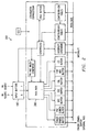
- FIG. 1 is a block diagram illustrating a slot-aligned IQ buffer 100 according to one embodiment of the present invention.
- the slot-aligned IQ buffer 100 is a triple data buffer system that allows vector processing of simultaneous frames of overlaying data in which the frames do not have the same starting position.
- a first data buffer 102, second data buffer 104 and third data buffer 106 allow the processing engine, such as a DSP associated with the CCP discussed herein above, to slide the selection of the vector to be processed so that it aligns with the framing of the data.
- CDMA and WCDMA communications employ overlaying coded data streams, each having its own frame timing.
- the slot-aligned IQ buffer 100 is particularly advantageous for CDMA and WCDMA systems because it allows for vastly simplified processing hardware.
- a WCDMA vector chip processor would require significant additional hardware just to support the compressed mode of operation in WCDMA.
- the slot-aligned IQ buffer 100 therefore allows for changing the way data is processed cleanly at boundaries in the data without requiring additional hardware to accommodate such changes.
- the slot-aligned IQ buffer 100 can be seen to include three 16-chip buffers 102, 104, 106.
- the buffers 102, 104, 106 are filled circularly; and each buffer 102, 104, 106 contains 64 (4x oversampled) samples of 12-bits (6 for I and 6 for Q).
- the one which holds the next 16 chips is used to access the extra chips which are not in the current buffer.
- the alignment of the task's frame determines the starting chip to be processed.
- the next 15 chips are then required to implement the correlator vector processing which is 16 chips wide. At most, 15 more chips might be required from the next buffer.
- There are three buffers 102, 104, 106 such that when the data in one buffer is processed, the next buffer can be used to access extra chips for processing while the third can be filled with incoming data.
- the first level of multiplexing 108 selects two of the three buffers 102, 104, 106, in order to select chips for processing.
- the second level of multiplexing 110a, b selects the sample number (0, 1, 2, 3 of the 4x oversamples) required.
- the third level of multiplexing 112a, b selects the correct chips for the alignment of the slot from two buffers. This last stage of multiplexing 112a, b, is done with a barrel shifter to achieve a smaller implementation than that which can be provided when using simple brute-force multiplexing techniques.
- Figure 2 is a top-level block diagram illustrating a correlator co-processor system 200 in communication with a pair of slot-aligned IQ buffers 100 while Figure 3 illustrates a more detailed block diagram for the data path portion 300 of the correlator co-processor system 200 depicted in Figure 2.
- the CCP system 200 when using single or even double data buffers, the CCP system 200 requires four adder trees 302 (2 for on-time and 2 for late-time) for information processing.
- the CCP system 200 requires a single adder tree for on-time and a single adder tree for late-time information processing.
- triple data buffer 100 Without the triple data buffer 100, additional adder trees are necessary to accommodate information processing when the slot timing does not align with the 16-chip processing timing and there is a symbol boundary in the 16 chips.
- Use of triple data buffers was found to reduce overall power requirements associated with correlations over the double buffer feeding additional adder trees.
- the pseudo-noise (PN) generator 304 can also be simplified to one which produces offset spaced 16 apart rather than one which simply produces any offset. Further, logic generally necessary to wrap data around to the beginning of the PN sequence can be eliminated, along with the linear feedback shift register (LFSR) implementation of the PN generator 304, since a window of sequential search hypotheses (+1 advance) no longer requires a PN sequence with the +1 advance feature.
- LFSR linear feedback shift register
- the CCP system 100 hardware must be alerted as to the direction (+/-) and the new sample position. In the worst case condition, extra processing of another 16 chips must be accomplished at the same time as the current 16 chips. Because there is another tree 302 available since the late-time tree is not used for fingers, the number of trees 302 is adequate. Use of the present triple data buffer 100 scheme for the CCP system 100 will operate to retain the foregoing information processing characteristics, even when the first chip being processed is the first chip in the buffer 100 and the timing goes from 0 to 3 (earlier).
- CCP system 100 design is simplified when implemented using the present slot-aligned IQ buffer 100.
- the adder trees 302 can be easily split into one, two, and four results without worry about where the symbol boundary is located.
- coherent adder trees required for space-time transmit diversity (STTD) pilot accumulations was found to be simplified as was pilot de-rotation bit alignments since pilot symbols align within slot and 16-chip windows.
- STTD space-time transmit diversity
- Figure 4 is a diagram illustrating data flow through a series of shift registers 400, 402, 404, suitable to implement a slot-aligned IQ buffer system 100 according to one embodiment of the present invention. Twelve bits of IQ data are communicated to the first buffer 400 and are left shifted until the entire buffer 400 is full. The next IQ data received are then communicated into the next buffer 402 and so on.
- FIG. 5 is a diagram illustrating data flow through a group of load enabled registers 500, 502, 504, suitable to implement a slot-aligned IQ buffer system 100 according to yet another embodiment of the present invention. This embodiment is preferred over the embodiment shown in Figure 4 since this embodiment was found to require lower power to provide a working system. Twelve bits of IQ data are loaded into a desired buffer (register) location. Once loaded, the IQ data does not shift, but remains in its present location until it is read or overwritten. The twelve IQ data lines 510 are connected to each sample register 500, 502, 504 in parallel. A control block 520 enables the proper register 500, 502, 504 in which to load a sequence of data.
- the present invention presents a significant advancement in the art of CDMA and WCDMA information processing.
- a slot-aligned IQ buffer architecture has been implemented to accommodate easy and simple processing of data using minimal hardware resources, even when compressed mode and change of services occur at slot boundaries.
- this invention has been described in considerable detail in order to provide those skilled in the data communication art with the information needed to apply the novel principles and to construct and use such specialized components as are required.
- the present invention represents a significant departure from the prior art in construction and operation.
Landscapes
- Engineering & Computer Science (AREA)
- Computer Networks & Wireless Communication (AREA)
- Signal Processing (AREA)
- Time-Division Multiplex Systems (AREA)
Abstract
Description
- This invention relates generally to data communication systems and methods, and more particularly to a minimally sized data buffer that allows vector processing of simultaneous frames of overlaying data in which the frames do not have the same starting position.
- When using a data communication system based on bursts (packets), the generic format of a frame consists of a preamble at the beginning of each burst. Some communication protocols additionally include data and end-of-frame. The preamble is used to signify (recognize) the start of transmission. All nodes on a network traditionally use the same preamble and the same end-of-frame. Each node, therefore, is required to decode at least the beginning of the data to identify if this message is addressed to itself. Decoding efforts importantly require a real-time computational complexity. Further, traditional data communication processes are made even more complex and time consuming due to the necessity to utilize collision detection and resolve techniques.
- Further, in code division multiple access (CDMA) systems, as well as others, there are overlaying coded data streams, each having its own frame timing. In view of the foregoing, it is therefore desirable to provide a technique to minimize or even reduce communication system real-time computational complexity and hardware requirements associated with processing simultaneous frames of overlaying data in which the frames do not have the same starting position for such systems. One solution could include using a double buffer scheme, but such a scheme does not address the foregoing undesirable hardware complexity issues.
- The present invention is directed to a triple data buffer for supporting high bit rate data communication systems such as the correlator co-processor (CCP) disclosed in U.S. Patent Application Serial Number 09/607,410 entitled "Correlator Co-Processor For CDMA RAKE Receiver Operations", and filed on June 30, 2000, by Katherine G. Brown et al.
- The CCP is capable of receiving multiple in-phase (I) and quadrature (Q) signal samples from multiple sources to accommodate antenna diversity wherein I and Q samples may be 6-bits or more. The I and Q samples further represent multiple overlaying channels, each of which have several multi-path elements, the aggregate data rate being possibly greater than the chip rate. The triple data buffer is a slot-aligned IQ buffer comprising three 16-chip buffers which are filled circularly. According to one embodiment, each of the 16-chip buffers contains 64 (4x oversampled) samples of 12-bits (6 for I and 6 for Q). When one of these 16-chip buffers is being processed, the one that holds the next 16 chips is used to access extra chips which are not in the current buffer. The alignment of the task's frame determines the starting chip to be processed and then the next 15 chips are required to do the correlator vector processing which is 16 chips wide. At most, 15 more chips might be required from the next buffer. There are three 16-chip buffers, so that one buffer can be processed at any time while the next can be used to access extra chips for processing, and the third can be filled with incoming data. Frame alignment is accomplished using three leve'ls of multiplexing. The first level selects a pair of buffers to be processed. The second level selects the sample number (0, 1, 2, 3 of the 4x oversamples) required. The third level selects the correct chips for the alignment of the slot and is implemented using a barrel shifter to provide a smaller configuration than necessary when using brute-force multiplexing techniques.
- In one aspect of the invention, an IQ data buffer is implemented to accommodate selection of IQ data bits which align to the frame/slot timing of each task.
- In still another aspect of the invention, an IQ data buffer is implemented to more easily accommodate compressed mode and change of service requirements when receiving data.
- In yet another aspect of the invention, an IQ data buffer is implemented that provides a simple control logic capable of rendering improved testing features over known architectures.
- Still another aspect of the invention is associated with an IQ data buffer that maximizes power efficiency when executing correlations.
- For a more complete understanding of the present invention, and the advantages thereof, reference is now made to the following detailed description of certain particular and illustrative embodiments and the features and aspects thereof, by way of example only, and with reference to the figures of the accompanying drawings in which:
- Figure 1 is a block diagram illustrating a slot-aligned IQ buffer according to one embodiment of the present invention;
- Figure 2 is a top-level block diagram illustrating a correlator co-processor system in communication with a pair of slot-aligned IQ buffers;
- Figure 3 illustrates a more detailed block diagram for the data path portion of the correlator co-processor system depicted in Figure 2;
- Figure 4 is a diagram illustrating data flow through a series of shift registers to implement a slot-aligned IQ buffer system according to one embodiment of the present invention; and
- Figure 5 is a diagram illustrating data flow through a group of load enabled registers to implement a slot-aligned IQ buffer system according to yet another embodiment of the present invention.
-
- While the above-identified drawing figure sets forth a particular embodiment, other embodiments of the present invention are also contemplated, as noted in the discussion. In all cases, this disclosure presents illustrated embodiments of the present invention by way of representation and not limitation. Numerous other modifications and embodiments can be devised by those skilled in the art which fall within the scope and spirit of the principles of this invention.
- Figure 1 is a block diagram illustrating a slot-aligned
IQ buffer 100 according to one embodiment of the present invention. The slot-alignedIQ buffer 100 is a triple data buffer system that allows vector processing of simultaneous frames of overlaying data in which the frames do not have the same starting position. Afirst data buffer 102,second data buffer 104 andthird data buffer 106 allow the processing engine, such as a DSP associated with the CCP discussed herein above, to slide the selection of the vector to be processed so that it aligns with the framing of the data. CDMA and WCDMA communications employ overlaying coded data streams, each having its own frame timing. The slot-alignedIQ buffer 100 is particularly advantageous for CDMA and WCDMA systems because it allows for vastly simplified processing hardware. Without this feature, a WCDMA vector chip processor would require significant additional hardware just to support the compressed mode of operation in WCDMA. The slot-alignedIQ buffer 100 therefore allows for changing the way data is processed cleanly at boundaries in the data without requiring additional hardware to accommodate such changes. - Looking again at Figure 1, the slot-aligned
IQ buffer 100 can be seen to include three 16-chip buffers buffers buffer chip buffers buffers - A certain amount of multiplexing is necessary in order to accomplish the frame alignment. The first level of
multiplexing 108 selects two of the threebuffers - Figure 2 is a top-level block diagram illustrating a
correlator co-processor system 200 in communication with a pair of slot-alignedIQ buffers 100 while Figure 3 illustrates a more detailed block diagram for thedata path portion 300 of thecorrelator co-processor system 200 depicted in Figure 2. According to one embodiment, when using single or even double data buffers, theCCP system 200 requires four adder trees 302 (2 for on-time and 2 for late-time) for information processing. When using the present triple data buffer implementation, theCCP system 200 requires a single adder tree for on-time and a single adder tree for late-time information processing. Without thetriple data buffer 100, additional adder trees are necessary to accommodate information processing when the slot timing does not align with the 16-chip processing timing and there is a symbol boundary in the 16 chips. Use of triple data buffers was found to reduce overall power requirements associated with correlations over the double buffer feeding additional adder trees. - Since the present
triple data buffer 100 is capable of allowing a 16-chip vector being processed to be aligned to the slot, the pseudo-noise (PN)generator 304 can also be simplified to one which produces offset spaced 16 apart rather than one which simply produces any offset. Further, logic generally necessary to wrap data around to the beginning of the PN sequence can be eliminated, along with the linear feedback shift register (LFSR) implementation of thePN generator 304, since a window of sequential search hypotheses (+1 advance) no longer requires a PN sequence with the +1 advance feature. - Generally, when a finger timing change is required, the
CCP system 100 hardware must be alerted as to the direction (+/-) and the new sample position. In the worst case condition, extra processing of another 16 chips must be accomplished at the same time as the current 16 chips. Because there is anothertree 302 available since the late-time tree is not used for fingers, the number oftrees 302 is adequate. Use of the presenttriple data buffer 100 scheme for theCCP system 100 will operate to retain the foregoing information processing characteristics, even when the first chip being processed is the first chip in thebuffer 100 and the timing goes from 0 to 3 (earlier). - In view of the foregoing,
CCP system 100 design is simplified when implemented using the present slot-alignedIQ buffer 100. The present inventor found, for example, although the same control logic needed to find the first symbol boundary in the 16 chips being processed is still necessary to find the alignment for the input multiplexers when using the present slot-alignedIQ buffer 100, the intricacies involved in SF=4 or 8, where there are multiple boundaries are removed. Now, theadder trees 302 can be easily split into one, two, and four results without worry about where the symbol boundary is located. Further, coherent adder trees required for space-time transmit diversity (STTD) pilot accumulations was found to be simplified as was pilot de-rotation bit alignments since pilot symbols align within slot and 16-chip windows. In view of the above, it can be seen the logic requirements to dump results from a tree is advantageously simplified leading to reduced risks and test time requirements for aCCP system 100. - When a service is changed on a slot boundary, or when the symbol finger (SF) is changed on a slot boundary in the case of compressed mode, having the
CCP system 100 hardware react and process the data after the boundary in a different way than the data before the boundary is simple when the processing of each of these is in a different iteration, as it would be with a slot-alignedIQ buffer 100. Without use of the present slot-alignedIQ buffer 100, the slot boundary will generally appear in the middle of a 16-chip processing window; and both types of processing will be required on the same iteration, requiring double the hardware resources. - Figure 4 is a diagram illustrating data flow through a series of
shift registers IQ buffer system 100 according to one embodiment of the present invention. Twelve bits of IQ data are communicated to thefirst buffer 400 and are left shifted until theentire buffer 400 is full. The next IQ data received are then communicated into thenext buffer 402 and so on. - Figure 5 is a diagram illustrating data flow through a group of load enabled
registers IQ buffer system 100 according to yet another embodiment of the present invention. This embodiment is preferred over the embodiment shown in Figure 4 since this embodiment was found to require lower power to provide a working system. Twelve bits of IQ data are loaded into a desired buffer (register) location. Once loaded, the IQ data does not shift, but remains in its present location until it is read or overwritten. The twelveIQ data lines 510 are connected to eachsample register control block 520 enables theproper register - In view of the above, it can be seen the present invention presents a significant advancement in the art of CDMA and WCDMA information processing. A slot-aligned IQ buffer architecture has been implemented to accommodate easy and simple processing of data using minimal hardware resources, even when compressed mode and change of services occur at slot boundaries. Further, this invention has been described in considerable detail in order to provide those skilled in the data communication art with the information needed to apply the novel principles and to construct and use such specialized components as are required. In view of the foregoing descriptions, it should further be apparent that the present invention represents a significant departure from the prior art in construction and operation. However, while particular embodiments of the present invention have been described herein in detail, it is to be understood that various alterations, modifications and substitutions can be made therein without departing in any way from the spirit and scope of the present invention. For example, although various embodiments have been presented herein with reference to particular functional architectures and algorithmic characteristics, the present inventive structures and methods are not necessarily limited to such a particular architecture or set of characteristics as used herein. It shall be understood the embodiments described herein above can be implemented using either gates or memory elements. Implementing the invention using memory, for example, would provide the same results as when implementing the invention using gates.
Claims (18)
- A slot-aligned IQ data buffer for high bit rate communication systems comprising:a first data buffer;a second data buffer;a third data buffer;a first data multiplexer arranged for communication with the first data buffer, the second data buffer and the third data buffer and operable to select a pair of data buffers in response to a desired time window;a second data multiplexer arranged for communication with the first data multiplexer and operable to select a single on-time data sample in response to a desired sample number;a third data multiplexer arranged for communication with the first data multiplexer and operable to select a single late-time data sample in response to a desired sample number;a first barrel shifter arranged for communication with the second data multiplexer and operable to select chips that are slot-aligned with incoming frames of data to generate slot-aligned on-time data samples; anda second barrel shifter arranged for communication with the third data multiplexer and operable to select chips that are slot-aligned with incoming frames of data to generate slot-aligned late-time data samples.
- The slot-aligned IQ data buffer according to claim 1, wherein each data buffer is configured to store 64 samples of 6 in-phase bits and 64 samples of 6 quadrature bits.
- The slot-aligned IQ data buffer according to claim 1, wherein the first, second and third data buffers are configured to be circularly filled with incoming data.
- The slot-aligned IQ data buffer according to claim 1, wherein the first multiplexer is a 3 to 1 multiplexer.
- The slot-aligned IQ data buffer according to claim 4, wherein the second and third multiplexers are 4 to 1 multiplexers.
- The slot-aligned IQ data buffer according to claim 1, wherein two of the data buffers are configured to store 16-chip wide vector data that is capable of being accessed simultaneously during storage of incoming data in the remaining data buffer to provide on-time and late-time energy data.
- A triple data buffer system for high bit rate communication systems comprising:means for storing first signal samples associated with 16 chips of 4x oversampled in-phase bits and 4x oversampled quadrature bits;means for storing second signal samples associated with 16 chips of 4x oversampled in-phase bits and 4x oversampled quadrature bits;means for storing third signal samples associated with 16 chips of 4x oversampled in-phase bits and 4x oversampled quadrature bits;first multiplexing means for selecting signal samples from the stored signal samples in response to a desired time window;second multiplexing means for selecting on-time data samples from the signal samples selected in response to a desired time window;third multiplexing means for selecting late-time data samples from the signal samples selected in response to a desired time window;first barrel shifting means for selecting chips that are slot-aligned with incoming frames of data to generate slot-aligned on-time data samples; andsecond barrel shifting means for selecting chips that are slot-aligned with incoming frames of data to generate slot-aligned late-time data samples.
- The triple data buffer system according to claim 7, wherein each means for storing signal samples is capable of storing 64 samples of 6 in-phase bits and 64 samples of 6 quadrature bits.
- The triple data buffer system according to claim 7, wherein the first, second and third means for storing signal samples are configured to be circularly filled with incoming data.
- The triple data buffer system according to claim 7, wherein the first multiplexing means is a 3 to 1 multiplexer.
- The triple data buffer system according to claim 10, wherein the second and third multiplexing means are 4 to 1 multiplexers.
- The triple data buffer system according to claim 7, wherein two of the means for storing signal samples are configured to store 16-chip wide vector data that is capable of being accessed simultaneously during storage of incoming data in the remaining means for storing signal samples to provide on-time and late-time energy data.
- A triple data buffer system comprising:a first chip storage buffer;a second chip storage buffer;a third chip storage buffer, wherein the first, second and third chip storage buffers are configured to store in combination, forty-eight 4x oversampled contiguous chips;a first multiplexer configured to multiplex the first, second and third chip storage buffers to select thirty-one 4x oversampled ½-chips within a desired time window;a second multiplexer configured to multiplex the first multiplexer to select one sample of thirty-one ½-chips from the thirty-one 4x oversampled ½-chips;a third multiplexer configured to multiplex the first multiplexer to select one sample of thirty-one ½-chips from the thirty-one 4x oversampled ½-chips;a first barrel shifter configured to shift bits associated with the sample selected by the second multiplexer to generate 16 slot-aligned on-time samples; anda second barrel shifter configured to shift bits associated with the sample selected by the third multiplexer to generate 16 slot-aligned late-time samples.
- The triple data buffer system according to claim 13, wherein each chip storage buffer is configured to store 64 samples of 6 in-phase bits and 64 samples of 6 quadrature bits.
- The triple data buffer system according to claim 13, wherein the first, second and third chip storage buffers are configured to be circularly filled with incoming data.
- The triple data buffer system according to claim 13, wherein the first multiplexer is a 3 to 1 multiplexer.
- The triple data buffer system according to claim 13, wherein the second and third multiplexers are 4 to 1 multiplexers.
- The triple data buffer system according to claim 13, wherein two of the chip storage buffers are configured to store 16-chip wide vector data that is capable of being accessed simultaneously during storage of incoming data in the remaining chip storage buffer to provide on-time and late-time energy data.
Applications Claiming Priority (2)
| Application Number | Priority Date | Filing Date | Title |
|---|---|---|---|
| US648184 | 2000-08-25 | ||
| US09/648,184 US6721295B1 (en) | 2000-08-25 | 2000-08-25 | Triple data system for high data rate communication systems |
Publications (3)
| Publication Number | Publication Date |
|---|---|
| EP1182802A2 true EP1182802A2 (en) | 2002-02-27 |
| EP1182802A3 EP1182802A3 (en) | 2006-12-13 |
| EP1182802B1 EP1182802B1 (en) | 2017-04-19 |
Family
ID=24599747
Family Applications (1)
| Application Number | Title | Priority Date | Filing Date |
|---|---|---|---|
| EP01000399.4A Expired - Lifetime EP1182802B1 (en) | 2000-08-25 | 2001-08-22 | Triple data buffer system for high data rate communication systems |
Country Status (2)
| Country | Link |
|---|---|
| US (1) | US6721295B1 (en) |
| EP (1) | EP1182802B1 (en) |
Cited By (3)
| Publication number | Priority date | Publication date | Assignee | Title |
|---|---|---|---|---|
| US20110276736A1 (en) * | 2006-02-14 | 2011-11-10 | Broadcom Corporation | Method and system for a rfic master |
| CN111143514A (en) * | 2019-12-27 | 2020-05-12 | 北京百度网讯科技有限公司 | Method and apparatus for generating information |
| CN111290305A (en) * | 2018-12-06 | 2020-06-16 | 航天科工惯性技术有限公司 | Multi-channel digital quantity acquisition and processing anti-collision method and system for multiple sets of inertial navigation systems |
Families Citing this family (7)
| Publication number | Priority date | Publication date | Assignee | Title |
|---|---|---|---|---|
| JP2003069517A (en) * | 2001-08-29 | 2003-03-07 | Fujitsu Ltd | Signal processing device, signal processing method, and multiplexing device |
| US7463671B2 (en) * | 2002-02-19 | 2008-12-09 | Marvell World Trade Ltd. | Rake receiver interface |
| US7406102B2 (en) * | 2002-07-03 | 2008-07-29 | Freescale Semiconductor, Inc. | Multi-mode method and apparatus for performing digital modulation and demodulation |
| US7107014B2 (en) * | 2002-10-24 | 2006-09-12 | Nokia Corporation | Transporting power control information |
| US7656905B2 (en) * | 2002-12-24 | 2010-02-02 | Samir Sheth | Apparatus and method for aggregation and transportation of gigabit ethernet and other packet based data formats |
| US7782778B2 (en) * | 2002-12-24 | 2010-08-24 | Samir Satish Sheth | Apparatus and method for fibre channel distance extension embedded within an optical transport system |
| US7243209B2 (en) * | 2005-01-27 | 2007-07-10 | International Business Machines Corporation | Apparatus and method for speeding up access time of a large register file with wrap capability |
Citations (2)
| Publication number | Priority date | Publication date | Assignee | Title |
|---|---|---|---|---|
| US5867527A (en) | 1994-09-30 | 1999-02-02 | Qualcomm Incorporated | Method of searching for a bursty signal |
| EP1128565A2 (en) | 2000-02-18 | 2001-08-29 | Texas Instruments Incorporated | Correlator co-processor for CDMA rake receiver |
Family Cites Families (9)
| Publication number | Priority date | Publication date | Assignee | Title |
|---|---|---|---|---|
| KR100192269B1 (en) * | 1996-03-25 | 1999-06-15 | 구자홍 | Variable length code decoder |
| US6194950B1 (en) * | 1997-08-28 | 2001-02-27 | Lucent Technologies Inc. | High-speed CMOS multiplexer |
| EP0935204A3 (en) * | 1998-02-05 | 2001-02-28 | Texas Instruments Incorporated | Programmable correlator coprocessor |
| US6611512B1 (en) * | 1998-10-14 | 2003-08-26 | Agere Systems Inc. | Apparatus and method for scheduling correlation operations of a DS-CDMA shared correlator |
| US6405273B1 (en) * | 1998-11-13 | 2002-06-11 | Infineon Technologies North America Corp. | Data processing device with memory coupling unit |
| US6502152B1 (en) * | 1999-03-08 | 2002-12-31 | Texas Instruments Incorporated | Dual interrupt vector mapping |
| US6473442B1 (en) * | 1999-04-12 | 2002-10-29 | Telefonaktiebolaget Lm Ericsson (Publ) | Communications system and method for matching and balancing the bit rates of transport channels to the bit rate of a physical channel |
| US6404758B1 (en) * | 1999-04-19 | 2002-06-11 | Ericsson, Inc. | System and method for achieving slot synchronization in a wideband CDMA system in the presence of large initial frequency errors |
| KR100390242B1 (en) * | 1999-06-29 | 2003-07-07 | 주식회사 하이닉스반도체 | Input buffer |
-
2000
- 2000-08-25 US US09/648,184 patent/US6721295B1/en not_active Expired - Lifetime
-
2001
- 2001-08-22 EP EP01000399.4A patent/EP1182802B1/en not_active Expired - Lifetime
Patent Citations (2)
| Publication number | Priority date | Publication date | Assignee | Title |
|---|---|---|---|---|
| US5867527A (en) | 1994-09-30 | 1999-02-02 | Qualcomm Incorporated | Method of searching for a bursty signal |
| EP1128565A2 (en) | 2000-02-18 | 2001-08-29 | Texas Instruments Incorporated | Correlator co-processor for CDMA rake receiver |
Cited By (5)
| Publication number | Priority date | Publication date | Assignee | Title |
|---|---|---|---|---|
| US20110276736A1 (en) * | 2006-02-14 | 2011-11-10 | Broadcom Corporation | Method and system for a rfic master |
| US8161217B2 (en) * | 2006-02-14 | 2012-04-17 | Broadcom Corporation | Method and system for a RFIC master |
| CN111290305A (en) * | 2018-12-06 | 2020-06-16 | 航天科工惯性技术有限公司 | Multi-channel digital quantity acquisition and processing anti-collision method and system for multiple sets of inertial navigation systems |
| CN111290305B (en) * | 2018-12-06 | 2021-05-04 | 航天科工惯性技术有限公司 | Multi-channel digital quantity acquisition and processing anti-collision method and system for multiple sets of inertial navigation systems |
| CN111143514A (en) * | 2019-12-27 | 2020-05-12 | 北京百度网讯科技有限公司 | Method and apparatus for generating information |
Also Published As
| Publication number | Publication date |
|---|---|
| US6721295B1 (en) | 2004-04-13 |
| EP1182802B1 (en) | 2017-04-19 |
| EP1182802A3 (en) | 2006-12-13 |
Similar Documents
| Publication | Publication Date | Title |
|---|---|---|
| EP1338097B1 (en) | Method and apparatus for processing a received signal in a communications system | |
| US6721371B1 (en) | One sample per symbol high rate programmable parallel architecture for digital demodulation | |
| US7145938B2 (en) | Apparatus producing continuous stream of correlation values | |
| US6163563A (en) | Digital communication system for high-speed complex correlation | |
| US6721295B1 (en) | Triple data system for high data rate communication systems | |
| CN1650590B (en) | Flexible correlation and queuing in CDMA communication systems | |
| US7130331B2 (en) | Method and apparatus for searching time-division multiplexed synchronization sequences | |
| US6779009B1 (en) | Enhanced time-shared data correlator architecture and method | |
| CN1157074C (en) | Baseband signal demodulating apparatus and method in mobile radio communication system | |
| US6480527B1 (en) | CDMA demodulating method and demodulator | |
| US8027375B2 (en) | Shared filter design for pilot symbol averaging in rake fingers in WCDMA systems | |
| US6014405A (en) | Spread spectrum multipath receiver without a tracking loop | |
| US20050169353A1 (en) | Post despreading interpolation in CDMA systems | |
| CN101369823A (en) | Rake receiver, path searcher and combining device and mobile communication device | |
| JP2002135168A (en) | RACH receiver | |
| EP1561288B1 (en) | Memory based device and method for channel estimation in a digital communication receiver | |
| KR101157108B1 (en) | Correlator for primary cell search using memory architecture | |
| JP3869674B2 (en) | Sliding correlator for spread spectrum communication | |
| US20020094021A1 (en) | Symbol combining method for reducing the number of FIFO registers of finger, rake receiver and method for driving the rake receiver | |
| EP0945992A1 (en) | CDMA array processor | |
| KR100327143B1 (en) | Cdma receiver with a reduced number of required high speed adders | |
| US20020061057A1 (en) | Digital filter | |
| EP1408621A1 (en) | Cdma reception apparatus and cdma reception method | |
| KR100313924B1 (en) | Apparatus and Method for searching Signal in Mobile Communication System | |
| JPH1065575A (en) | Repetitive transmission signal synthesis circuit and symbol synthesizer |
Legal Events
| Date | Code | Title | Description |
|---|---|---|---|
| PUAI | Public reference made under article 153(3) epc to a published international application that has entered the european phase |
Free format text: ORIGINAL CODE: 0009012 |
|
| AK | Designated contracting states |
Kind code of ref document: A2 Designated state(s): AT BE CH CY DE DK ES FI FR GB GR IE IT LI LU MC NL PT SE TR |
|
| AX | Request for extension of the european patent |
Free format text: AL;LT;LV;MK;RO;SI |
|
| PUAL | Search report despatched |
Free format text: ORIGINAL CODE: 0009013 |
|
| AK | Designated contracting states |
Kind code of ref document: A3 Designated state(s): AT BE CH CY DE DK ES FI FR GB GR IE IT LI LU MC NL PT SE TR |
|
| AX | Request for extension of the european patent |
Extension state: AL LT LV MK RO SI |
|
| RIC1 | Information provided on ipc code assigned before grant |
Ipc: H04B 1/707 20060101ALI20061108BHEP Ipc: H04B 7/26 20060101AFI20011023BHEP |
|
| 17P | Request for examination filed |
Effective date: 20070613 |
|
| AKX | Designation fees paid |
Designated state(s): DE FR GB |
|
| 17Q | First examination report despatched |
Effective date: 20090407 |
|
| REG | Reference to a national code |
Ref country code: DE Ref legal event code: R079 Ref document number: 60150399 Country of ref document: DE Free format text: PREVIOUS MAIN CLASS: H04B0007260000 Ipc: H04B0001711500 |
|
| GRAP | Despatch of communication of intention to grant a patent |
Free format text: ORIGINAL CODE: EPIDOSNIGR1 |
|
| RIC1 | Information provided on ipc code assigned before grant |
Ipc: H04B 1/707 20060101ALI20161027BHEP Ipc: H04B 1/7115 20110101AFI20161027BHEP Ipc: H04B 7/26 20060101ALI20161027BHEP |
|
| INTG | Intention to grant announced |
Effective date: 20161123 |
|
| RAP1 | Party data changed (applicant data changed or rights of an application transferred) |
Owner name: TEXAS INSTRUMENTS INC. |
|
| GRAS | Grant fee paid |
Free format text: ORIGINAL CODE: EPIDOSNIGR3 |
|
| GRAA | (expected) grant |
Free format text: ORIGINAL CODE: 0009210 |
|
| AK | Designated contracting states |
Kind code of ref document: B1 Designated state(s): DE FR GB |
|
| REG | Reference to a national code |
Ref country code: GB Ref legal event code: FG4D |
|
| REG | Reference to a national code |
Ref country code: DE Ref legal event code: R096 Ref document number: 60150399 Country of ref document: DE |
|
| REG | Reference to a national code |
Ref country code: FR Ref legal event code: PLFP Year of fee payment: 17 |
|
| PGFP | Annual fee paid to national office [announced via postgrant information from national office to epo] |
Ref country code: GB Payment date: 20170725 Year of fee payment: 17 Ref country code: DE Payment date: 20170825 Year of fee payment: 17 Ref country code: FR Payment date: 20170720 Year of fee payment: 17 |
|
| REG | Reference to a national code |
Ref country code: DE Ref legal event code: R097 Ref document number: 60150399 Country of ref document: DE |
|
| PLBE | No opposition filed within time limit |
Free format text: ORIGINAL CODE: 0009261 |
|
| STAA | Information on the status of an ep patent application or granted ep patent |
Free format text: STATUS: NO OPPOSITION FILED WITHIN TIME LIMIT |
|
| 26N | No opposition filed |
Effective date: 20180122 |
|
| REG | Reference to a national code |
Ref country code: DE Ref legal event code: R119 Ref document number: 60150399 Country of ref document: DE |
|
| GBPC | Gb: european patent ceased through non-payment of renewal fee |
Effective date: 20180822 |
|
| PG25 | Lapsed in a contracting state [announced via postgrant information from national office to epo] |
Ref country code: DE Free format text: LAPSE BECAUSE OF NON-PAYMENT OF DUE FEES Effective date: 20190301 |
|
| PG25 | Lapsed in a contracting state [announced via postgrant information from national office to epo] |
Ref country code: FR Free format text: LAPSE BECAUSE OF NON-PAYMENT OF DUE FEES Effective date: 20180831 |
|
| PG25 | Lapsed in a contracting state [announced via postgrant information from national office to epo] |
Ref country code: GB Free format text: LAPSE BECAUSE OF NON-PAYMENT OF DUE FEES Effective date: 20180822 |