EP1182756A2 - Semiconductor laser device having lower threshold current - Google Patents
Semiconductor laser device having lower threshold current Download PDFInfo
- Publication number
- EP1182756A2 EP1182756A2 EP01118280A EP01118280A EP1182756A2 EP 1182756 A2 EP1182756 A2 EP 1182756A2 EP 01118280 A EP01118280 A EP 01118280A EP 01118280 A EP01118280 A EP 01118280A EP 1182756 A2 EP1182756 A2 EP 1182756A2
- Authority
- EP
- European Patent Office
- Prior art keywords
- semiconductor laser
- layer
- layers
- gaas
- active layer
- Prior art date
- Legal status (The legal status is an assumption and is not a legal conclusion. Google has not performed a legal analysis and makes no representation as to the accuracy of the status listed.)
- Granted
Links
- 239000004065 semiconductor Substances 0.000 title claims abstract description 90
- 229910001218 Gallium arsenide Inorganic materials 0.000 claims description 59
- 229910052757 nitrogen Inorganic materials 0.000 claims description 49
- 230000004888 barrier function Effects 0.000 claims description 45
- 239000000758 substrate Substances 0.000 claims description 28
- 238000000034 method Methods 0.000 claims description 26
- 238000004519 manufacturing process Methods 0.000 claims description 8
- 229910052787 antimony Inorganic materials 0.000 claims description 4
- 238000000151 deposition Methods 0.000 claims 10
- 229910052785 arsenic Inorganic materials 0.000 claims 5
- 229910052733 gallium Inorganic materials 0.000 claims 4
- 229910052738 indium Inorganic materials 0.000 claims 3
- 230000008021 deposition Effects 0.000 claims 1
- 230000003287 optical effect Effects 0.000 abstract description 20
- IJGRMHOSHXDMSA-UHFFFAOYSA-N Atomic nitrogen Chemical compound N#N IJGRMHOSHXDMSA-UHFFFAOYSA-N 0.000 description 91
- 238000005424 photoluminescence Methods 0.000 description 68
- 230000004907 flux Effects 0.000 description 31
- 238000002474 experimental method Methods 0.000 description 29
- 238000010438 heat treatment Methods 0.000 description 28
- 229910000530 Gallium indium arsenide Inorganic materials 0.000 description 13
- 238000005253 cladding Methods 0.000 description 13
- 239000004094 surface-active agent Substances 0.000 description 10
- 238000005259 measurement Methods 0.000 description 8
- 239000000203 mixture Substances 0.000 description 7
- RBFQJDQYXXHULB-UHFFFAOYSA-N arsane Chemical compound [AsH3] RBFQJDQYXXHULB-UHFFFAOYSA-N 0.000 description 6
- 229910000070 arsenic hydride Inorganic materials 0.000 description 6
- 125000004429 atom Chemical group 0.000 description 6
- 238000001451 molecular beam epitaxy Methods 0.000 description 6
- 239000000470 constituent Substances 0.000 description 4
- 239000013078 crystal Substances 0.000 description 4
- 230000005012 migration Effects 0.000 description 4
- 238000013508 migration Methods 0.000 description 4
- 229910004205 SiNX Inorganic materials 0.000 description 3
- 230000006870 function Effects 0.000 description 3
- 238000002488 metal-organic chemical vapour deposition Methods 0.000 description 3
- 238000012360 testing method Methods 0.000 description 3
- 230000007423 decrease Effects 0.000 description 2
- 230000007547 defect Effects 0.000 description 2
- 238000013461 design Methods 0.000 description 2
- 238000009792 diffusion process Methods 0.000 description 2
- 238000005530 etching Methods 0.000 description 2
- 238000000171 gas-source molecular beam epitaxy Methods 0.000 description 2
- 239000012535 impurity Substances 0.000 description 2
- 238000002347 injection Methods 0.000 description 2
- 239000007924 injection Substances 0.000 description 2
- 238000002156 mixing Methods 0.000 description 2
- 230000008569 process Effects 0.000 description 2
- 229910000980 Aluminium gallium arsenide Inorganic materials 0.000 description 1
- 229910017401 Au—Ge Inorganic materials 0.000 description 1
- 238000003917 TEM image Methods 0.000 description 1
- 238000005054 agglomeration Methods 0.000 description 1
- 230000002776 aggregation Effects 0.000 description 1
- 230000004075 alteration Effects 0.000 description 1
- 238000000137 annealing Methods 0.000 description 1
- 230000008901 benefit Effects 0.000 description 1
- 230000005540 biological transmission Effects 0.000 description 1
- 230000015556 catabolic process Effects 0.000 description 1
- 238000004891 communication Methods 0.000 description 1
- 238000007796 conventional method Methods 0.000 description 1
- 238000001816 cooling Methods 0.000 description 1
- 238000005336 cracking Methods 0.000 description 1
- 238000006731 degradation reaction Methods 0.000 description 1
- 230000000694 effects Effects 0.000 description 1
- 230000006872 improvement Effects 0.000 description 1
- 238000010348 incorporation Methods 0.000 description 1
- 238000009413 insulation Methods 0.000 description 1
- 238000011835 investigation Methods 0.000 description 1
- 239000000463 material Substances 0.000 description 1
- 238000012986 modification Methods 0.000 description 1
- 230000004048 modification Effects 0.000 description 1
- 150000002831 nitrogen free-radicals Chemical class 0.000 description 1
- 239000013307 optical fiber Substances 0.000 description 1
- 230000001590 oxidative effect Effects 0.000 description 1
- 125000004437 phosphorous atom Chemical group 0.000 description 1
- 230000009467 reduction Effects 0.000 description 1
- 238000005204 segregation Methods 0.000 description 1
- 239000000243 solution Substances 0.000 description 1
- 238000004227 thermal cracking Methods 0.000 description 1
- 238000005979 thermal decomposition reaction Methods 0.000 description 1
Images





Classifications
-
- H—ELECTRICITY
- H01—ELECTRIC ELEMENTS
- H01S—DEVICES USING THE PROCESS OF LIGHT AMPLIFICATION BY STIMULATED EMISSION OF RADIATION [LASER] TO AMPLIFY OR GENERATE LIGHT; DEVICES USING STIMULATED EMISSION OF ELECTROMAGNETIC RADIATION IN WAVE RANGES OTHER THAN OPTICAL
- H01S5/00—Semiconductor lasers
- H01S5/30—Structure or shape of the active region; Materials used for the active region
- H01S5/34—Structure or shape of the active region; Materials used for the active region comprising quantum well or superlattice structures, e.g. single quantum well [SQW] lasers, multiple quantum well [MQW] lasers or graded index separate confinement heterostructure [GRINSCH] lasers
- H01S5/343—Structure or shape of the active region; Materials used for the active region comprising quantum well or superlattice structures, e.g. single quantum well [SQW] lasers, multiple quantum well [MQW] lasers or graded index separate confinement heterostructure [GRINSCH] lasers in AIIIBV compounds, e.g. AlGaAs-laser, InP-based laser
-
- B—PERFORMING OPERATIONS; TRANSPORTING
- B82—NANOTECHNOLOGY
- B82Y—SPECIFIC USES OR APPLICATIONS OF NANOSTRUCTURES; MEASUREMENT OR ANALYSIS OF NANOSTRUCTURES; MANUFACTURE OR TREATMENT OF NANOSTRUCTURES
- B82Y20/00—Nanooptics, e.g. quantum optics or photonic crystals
-
- H—ELECTRICITY
- H01—ELECTRIC ELEMENTS
- H01S—DEVICES USING THE PROCESS OF LIGHT AMPLIFICATION BY STIMULATED EMISSION OF RADIATION [LASER] TO AMPLIFY OR GENERATE LIGHT; DEVICES USING STIMULATED EMISSION OF ELECTROMAGNETIC RADIATION IN WAVE RANGES OTHER THAN OPTICAL
- H01S5/00—Semiconductor lasers
- H01S5/10—Construction or shape of the optical resonator, e.g. extended or external cavity, coupled cavities, bent-guide, varying width, thickness or composition of the active region
- H01S5/18—Surface-emitting [SE] lasers, e.g. having both horizontal and vertical cavities
- H01S5/183—Surface-emitting [SE] lasers, e.g. having both horizontal and vertical cavities having only vertical cavities, e.g. vertical cavity surface-emitting lasers [VCSEL]
- H01S5/18308—Surface-emitting [SE] lasers, e.g. having both horizontal and vertical cavities having only vertical cavities, e.g. vertical cavity surface-emitting lasers [VCSEL] having a special structure for lateral current or light confinement
- H01S5/18311—Surface-emitting [SE] lasers, e.g. having both horizontal and vertical cavities having only vertical cavities, e.g. vertical cavity surface-emitting lasers [VCSEL] having a special structure for lateral current or light confinement using selective oxidation
-
- H—ELECTRICITY
- H01—ELECTRIC ELEMENTS
- H01S—DEVICES USING THE PROCESS OF LIGHT AMPLIFICATION BY STIMULATED EMISSION OF RADIATION [LASER] TO AMPLIFY OR GENERATE LIGHT; DEVICES USING STIMULATED EMISSION OF ELECTROMAGNETIC RADIATION IN WAVE RANGES OTHER THAN OPTICAL
- H01S5/00—Semiconductor lasers
- H01S5/30—Structure or shape of the active region; Materials used for the active region
- H01S5/32—Structure or shape of the active region; Materials used for the active region comprising PN junctions, e.g. hetero- or double- heterostructures
- H01S5/323—Structure or shape of the active region; Materials used for the active region comprising PN junctions, e.g. hetero- or double- heterostructures in AIIIBV compounds, e.g. AlGaAs-laser, InP-based laser
- H01S5/3235—Structure or shape of the active region; Materials used for the active region comprising PN junctions, e.g. hetero- or double- heterostructures in AIIIBV compounds, e.g. AlGaAs-laser, InP-based laser emitting light at a wavelength longer than 1000 nm, e.g. InP-based 1300 nm and 1500 nm lasers
- H01S5/32358—Structure or shape of the active region; Materials used for the active region comprising PN junctions, e.g. hetero- or double- heterostructures in AIIIBV compounds, e.g. AlGaAs-laser, InP-based laser emitting light at a wavelength longer than 1000 nm, e.g. InP-based 1300 nm and 1500 nm lasers containing very small amounts, usually less than 1%, of an additional III or V compound to decrease the bandgap strongly in a non-linear way by the bowing effect
-
- H—ELECTRICITY
- H01—ELECTRIC ELEMENTS
- H01S—DEVICES USING THE PROCESS OF LIGHT AMPLIFICATION BY STIMULATED EMISSION OF RADIATION [LASER] TO AMPLIFY OR GENERATE LIGHT; DEVICES USING STIMULATED EMISSION OF ELECTROMAGNETIC RADIATION IN WAVE RANGES OTHER THAN OPTICAL
- H01S5/00—Semiconductor lasers
- H01S5/30—Structure or shape of the active region; Materials used for the active region
- H01S5/32—Structure or shape of the active region; Materials used for the active region comprising PN junctions, e.g. hetero- or double- heterostructures
- H01S5/323—Structure or shape of the active region; Materials used for the active region comprising PN junctions, e.g. hetero- or double- heterostructures in AIIIBV compounds, e.g. AlGaAs-laser, InP-based laser
- H01S5/3235—Structure or shape of the active region; Materials used for the active region comprising PN junctions, e.g. hetero- or double- heterostructures in AIIIBV compounds, e.g. AlGaAs-laser, InP-based laser emitting light at a wavelength longer than 1000 nm, e.g. InP-based 1300 nm and 1500 nm lasers
- H01S5/32358—Structure or shape of the active region; Materials used for the active region comprising PN junctions, e.g. hetero- or double- heterostructures in AIIIBV compounds, e.g. AlGaAs-laser, InP-based laser emitting light at a wavelength longer than 1000 nm, e.g. InP-based 1300 nm and 1500 nm lasers containing very small amounts, usually less than 1%, of an additional III or V compound to decrease the bandgap strongly in a non-linear way by the bowing effect
- H01S5/32366—(In)GaAs with small amount of N
-
- H—ELECTRICITY
- H01—ELECTRIC ELEMENTS
- H01S—DEVICES USING THE PROCESS OF LIGHT AMPLIFICATION BY STIMULATED EMISSION OF RADIATION [LASER] TO AMPLIFY OR GENERATE LIGHT; DEVICES USING STIMULATED EMISSION OF ELECTROMAGNETIC RADIATION IN WAVE RANGES OTHER THAN OPTICAL
- H01S5/00—Semiconductor lasers
- H01S5/30—Structure or shape of the active region; Materials used for the active region
- H01S5/34—Structure or shape of the active region; Materials used for the active region comprising quantum well or superlattice structures, e.g. single quantum well [SQW] lasers, multiple quantum well [MQW] lasers or graded index separate confinement heterostructure [GRINSCH] lasers
- H01S5/343—Structure or shape of the active region; Materials used for the active region comprising quantum well or superlattice structures, e.g. single quantum well [SQW] lasers, multiple quantum well [MQW] lasers or graded index separate confinement heterostructure [GRINSCH] lasers in AIIIBV compounds, e.g. AlGaAs-laser, InP-based laser
- H01S5/34306—Structure or shape of the active region; Materials used for the active region comprising quantum well or superlattice structures, e.g. single quantum well [SQW] lasers, multiple quantum well [MQW] lasers or graded index separate confinement heterostructure [GRINSCH] lasers in AIIIBV compounds, e.g. AlGaAs-laser, InP-based laser emitting light at a wavelength longer than 1000nm, e.g. InP based 1300 and 1500nm lasers
Definitions
- the present invention relates to a semiconductor laser device having a lower threshold current.
- GaInAsP semiconductor laser device formed on an InP substrate is conventionally developed as a semiconductor laser device having an emission wavelength of 1.3 ⁇ m band, it has been a problem that the semiconductor materials used in the GaInAsP laser device has a poor characteristic temperature of the threshold current as low as 50K to 70K, which degrades the temperature characteristics of the laser device.
- the semiconductor laser module In order to dispose a semiconductor laser device in each of households as a light source, it is desired that the semiconductor laser module have a longer wavelength band and a superior temperature characteristic without using a cooling device, and also can be manufactured at a lower cost.
- the conventional high-strained semiconductor laser device as described above suffers from the higher amount of strain and a poor mixing capability of the constituent element, nitrogen (N), into the V-group elements due to the fact that nitrogen has a smaller radius of atoms. This involves an undesirable three-dimensional growth and a large number of crystal defects unless the growth temperature is lowered to a minimum, which however degrades the optical quality for the crystal structure.
- the high strained layer is difficult to grow with involving a longer-distance migration by using a molecular beam epitaxy (MBE) generally used for growing semiconductor layers.
- MBE molecular beam epitaxy
- the present invention provides a semiconductor laser device including a GaAs substrate and a laser structure overlying thereon and including a quantum well (QW) active layer structure, said QW active layer structure including a Ga x In 1-x As 1-y Sb y well layer wherein 0.3 ⁇ 1-x and 0.003 ⁇ y ⁇ 0.008 or a Ga x In 1-x A s1-y1-y2 N y1 Sb y2 well layer wherein 0.3 ⁇ 1-x, 0 ⁇ y1 ⁇ 0.03 and 0.002 ⁇ y2 ⁇ 0.06.
- QW quantum well
- the semiconductor laser device of the present invention it is preferable to suppress the migration of Group-III atoms to some extent because the Group-III atoms may grow in a three-dimensional structure due to agglomeration during growth of the same as a high-strained layer if the migration distance of the Group-III atoms is large.
- the present invention also provides a method for manufacturing the semiconductor device including the step of heat treating the layer structure of the laser structure at temperatures depending on the composition of the active layer, after epitaxial growth of the Ga x In 1-x A s1- y1-y2 N y1 Sb y2 well layer.
- the heat treatment is conducted at a temperature of 570 degrees C to 630 degrees C when 0 ⁇ y1 ⁇ 0.007 or at a temperature of 670 degrees C to 730 degrees C when 0.007 ⁇ y1 ⁇ 0.03.
- a conventional high-strained GaIn 0.39 As semiconductor laser device operates at an emission wavelength of 1.2 ⁇ m.
- the semiconductor laser device 40 includes a multi-layer structure formed on a (100) plane of an n-GaAs substrate and including an n-type GaAs (n-GaAs) buffer layer 44 having a thickness of 0.2 ⁇ m, an n-InGaP cladding layer 46 having a thickness of 1.5 ⁇ m, a GaAs optical confinement layer 48 having a thickness of 0.13 ⁇ m, a GaInAs active layer 50, a GaAs optical confinement layer 52 having a thickness of 0.13 ⁇ m, a p-InGaP cladding layer 54 having a thickness of 1.5 ⁇ m, and a p-GaAs contact layer 56 having a thickness of 0.35 ⁇ m.
- nitrogen (N) is generally added to a GaInAs layer, wherein In is about 40% in the Group-III elements, at about 0.6% in atomic ratio relative to the V-group elements, to obtain a strain of around 2.7% in the total strain of the GalnNAs semiconductor laser.
- This device suffers from the higher amount of strain and from poor mixing capability of the constituent element, nitrogen, into the V-group elements due to nitrogen having a smaller radius of atoms.
- This device thus involves a three-dimensional growth and a large number of crystal defects unless the epitaxial growth is conducted at a lower temperature, which degrades the optical quality for the crystal structure however.
- the techniques including (a) a lower-temperature growth, (b) a higher atomic ratio of V-group elements to Group-III elements, (c) a higher growth rate, and (d) using a surfactant.
- the technique using the surfactant is such that elements having a property of higher segregation feasibility, such as Sb, Te and Sn, are used in a MBE or MOCVD for reducing the surface energy and the surface diffusion length of the group-III atoms to thereby suppress the three-dimensional growth.
- This technique is described by M.Copel et al., in Phys.Rev.Lett.vol.63(1989) pp.632-635.
- the growth step is stopped or interrupted to dispose the surfactant on the underlying layer in an amount of 1 ML or less before growing the high-strained layer.
- the surfactant is not added, whereby the surfactant is floating on the surface of the high-strained layer without incorporating into the high-strained layer.
- the present inventor noticed the effectiveness of addition of Sb in a minute amount of about 0.2% to 2.5% with respect to the amount of V-group elements together with addition of a Group-III element during the growth of the high strained layer, without disposing the surfactant on the underlying layer before growing the high-strained layer.
- a GalnAsSb layer is formed in a 1.2- ⁇ m band GaInAs semiconductor laser device, whereas a GaInNAsSb layer is formed in a 1.3- ⁇ m band GaInNAs semiconductor laser device.
- Sb is added in a GaIn 0.39 As single quantum well (SQW) active layer, to thereby manufacture a 1.2- ⁇ m band semiconductor laser device.
- SQL single quantum well
- the MBE technique may be replaced by a MOCVD technique.
- a GaIn 0.39 As SQW layer has a higher compressive strain as high as 2.8%.
- the design thickness of the SQW layer structure is set at 7.3 nm, wherein the relationship between the critical thickness and the In content is calculated to obtain 4 nm for the critical thickness based on the theory presented by J.W.Matthews and A.E.Blakeslee for the GaInAs/GaAs semiconductor laser device.
- Sb is added only to a GaIn 0.39 As SQW layer to form a GaInAsSb SQW layer.
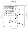
- the Sb flux (Torr) as a parameter, the photoluminescence (PL) dependency of the Sb flux was investigated.
- the results are shown in Fig. 5.
- amount of Sb flux or simply “Sb flux” as used herein means the intensity of the molecular beam of Sb incident onto the substrate and evaluated in terms of the partial pressure at the surface of the substrate.
- the growth conditions of the GaInAsSb layer in the experiments are as follows:
- PL photoluminescence
- GaAsSb layers were grown with different amounts of Sb flux, and the Sb contents (%) in the GaAsSb layers were measured. The results is shown in Fig. 6.
- the growth rate, the AsH 3 flux, and the growth temperature in the second experiments were identical to the epitaxial growth conditions of the GaInAsSb well layer of the first experiments.
- the composition of the GaInAsSb film resulted in Ga 0.61 In 0.39 As 0.9968 Sb 0.0032 , that means a minute amount of Sb was incorporated into the film.
- Sb does not act as a surfactant, and that Sb is incorporated in the GaInAs film to act as a quasi-surfactant.
- Sb has a function for lowering the surface energy, suppressing extension of the diffusion length, and suppressing the three-dimensional growth.
- the well layer had a compressive strain of 2.7% when the well layer had no Sb content (or made of GaIn 0.39 AsN 0.0044 ), and had a design thickness of 7.3 nm.
- the nitrogen radicals excited by a RF plasma source were used as the nitrogen source.
- a semi-insulating GaAs wafer is mounted on the GaInAsSb layer in a nitrogen ambient, in a face-to-face contact with the epitaxial layer side thereof, followed by an annealing step at a temperature of 650 degrees C for ten minutes.
- the semi-insulating GaAs wafer functions as a cap layer for preventing the escape of phosphorus atoms.
- Fig. 7 shows the Sb flux dependency of the PL intensity and the PL wavelength. It will be understood from Fig. 7 that a Sb flux of about 5x10 -7 to 1x10 -6 Torr is optimum for obtaining a higher PL intensity.
- a Sb flux of 1x10 -6 Torr provides a Sb content of 1.6% relative to the V-group elements, and the nitrogen content is calculated at 0.44% relative to the V-group elements based on the wavelength shift of the as-grown epitaxial layer occurring with the addition of nitrogen.
- Figs. 8A and 8B respectively show the TEM image photography of GaInNAsSb layers grown with the addition of Sb at amounts of Sb flux of 2x10 -7 Torr and 1x10 -6 Torr, respectively.
- the critical thickness between the two-dimensional structure and the three-dimensional structure can be improved by the Sb content due to the Sb acting as a quasi-surfactant in a GaInNAs/GaAs based semiconductor laser.
- the nitrogen content should be increased to some extent, which necessitates increase of the Sb content.
- the optimum Sb content depends on the composition of the layer, a larger N content generally increases the optimum Sb content.
- the emission wavelength is desirable to be increased up to 1.35 ⁇ m in consideration that WDM (wavelength division multiplexing) system is expected to develop into a 1.3 ⁇ m band wavelength. In such a case, the nitrogen content should be increased up to around 1.5% depending on the In content.
- the Sb content for allowing the semiconductor laser device to cover the 1.3 ⁇ m range should be between 0.2% and 6%.
- the fourth experiments are such that the wavelength is increased up to 1.3 ⁇ m by using a GaInNAsSb well layer.
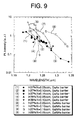
- the use of both GaInNAsSb well layer and GaAs barrier layer involved a problem in that the PL intensity in the vicinity of 1.3 ⁇ m decreases down to 1/20 compared to the PL intensity in the vicinity of 1.2 ⁇ m, as shown by the graphs (1) to (5) in Fig. 9.
- Fig. 9 shows the results of the present experiments wherein the well layers were formed for a variety of In contents and nitrogen contents for the GaInNAsSb layer. The results exhibited the tendency of reduction in the PL intensity along a specific curve for the different contents in the well layer so long as GaAs is used as the barrier layers.
- a plurality of laser structures were formed each including an n-GaAs buffer layer having a thickness of 0.2 ⁇ m, an n-In 0.47 Ga 0.53 P cladding layer having a thickness of 0.25 ⁇ m, a GaAs optical confinement layer having a thickness of 0.1 ⁇ m, a SQW active layer structure including a GaAs barrier layer having a thickness of 0.03 ⁇ m, a SQW layer having a thickness of 7.3 nm, and a GaAs barrier layer having a thickness of 0.03 ⁇ m, a GaAs optical confinement layer having a thickness of 0.1 ⁇ m, and a p-In 0.47 Ga 0.53 P cladding layer having thickness of 0.25 ⁇ m, which were consecutively formed in this order on a (100) plane of an n-GaAs substrate.
- the SQW layer is made of Ga x In 1-x N 1-y-0.016 As y Sb 0.016 .
- Some samples of the laser structures were formed at a growth temperature of 460 degrees C for the well layers and the barrier layers, with the In content in the GaInNAsSb well layer being 37%, the nitrogen flow rate being varied at 0.05 sccm, 0.10 sccm and 0.15 sccm.
- the other samples of the laser structures were also formed with the In content in the GaInNAsSb well layer being 39%, and the nitrogen flow rate at 0.05 sccm and 0.10 sccm, with the other conditions being maintained similar to the some samples.
- These samples of the laser structures were subjected to a heat treatment at a temperature of 500 to 700 degrees C in a nitrogen ambient for ten minutes for improvement of the crystallinity after the epitaxial growth.
- the resultant laser structures having those well layers and barrier layers are subjected to measurements of the PL wavelength and the PL intensity thereof.
- the results of the measurements are by the graphs (1) to (5) shown in Fig. 9, with the PL wavelength and the PL intensity (%) being plotted on abscissa and ordinate, respectively, for showing the PL wavelength dependency of the PL intensity.
- the PL intensity is plotted on arbitrary unit for showing the relative intensity between the samples.
- Tables 1 to 5 show the measured values plotted on the graphs (1) to (5), respectively.
- PL intensity increases by several times compared to the as-grown epitaxial layer without the high-temperature heat treatment, with an effect of decrease of the GaInNAs(Sb) layer, however, in the bandgap wavelength.
- the relationship between the PL wavelength and the PL intensity for the case of an In content of 37% and a nitrogen flow rate of 0.05 sccm is such that shown by the graph (1) wherein the wavelength of the as-grown layer is 1.222 ⁇ m whereas the wavelengths of the epitaxial layers subjected to the heat treatments at 550 degrees C and 650 degrees C are 1.21 ⁇ m and 1.18 ⁇ m, respectively.
- the PL intensity of the laser structure having GaAs barrier layers and a PL wavelength of 1.3 ⁇ m is remarkably lower compared to a GaInNAsSb well layer having a PL wavelength of 1.2 ⁇ m regardless of the composition of the well layer.
- the PL intensity is lower by 1/20, as shown in the graph (3).
- the lower PL intensity results from the degradation in the crystallinity of the epitaxial layers.
- the inventor examined the solution of the lower PL intensity by using a GaNAs barrier layers having the structure as will be detailed below.
- An n-GaAs buffer layer having a thickness of 0.2 ⁇ m, an n-In 0.47 Ga 0.53 P cladding layer having a thickness of 0.25 ⁇ m, a GaAs optical confinement layer having a thickness 0.1 ⁇ m a GaNAs barrier layer having a thickness of 0.03 ⁇ m, a SQW layer having a thickness of 7.3 nm, a GaNAs barrier layer having a thickness of 0.03 ⁇ m, a GaAs optical confinement layer having a thickness of 0.1 ⁇ m and a p-InGaP cladding layer having thickness of 0.25 ⁇ m were consecutively grown on a (100) plane of an n-GaAs substrate to form a layer structure implementing a laser structure.
- a plurality of laser structures having the layer structure described above were formed.
- the SQW layer is made of Ga x In 1-x N 1-y-0.016 As y Sb 0.016 similarly to the laser structure having GaAs barrier layers. While changing the In content in the SQW layers, the nitrogen content is changed in accordance therewith between 0.66% and 1.8%, or between 0.05 sccm and 0.15 sccm in terms of the nitrogen flow rate, in the GaNAs barrier layer.
- Some laser structures were formed with the In content in the GaInNAsSb well layer being fixed at 37%, with the nitrogen content being changed from 0.33% to 1.8% (or the nitrogen (N 2 ) flow rate between 0.05 sccm and 0.15 sccm), and other laser structures were formed with the In content being fixed at 39% and with the nitrogen flow rate being fixed at 0.05 sccm.
- the layers of these laser structures were subjected to a heat treatment, and the PL intensity and the PL wavelength were measured before and after the heat treatment. The results of the measurements are shown by graphs (6) to (9) in Fig. 9.
- the PL intensity of the as-grown epitaxial layers including a pair of GaNAs barrier layers is lower, the PL intensity increases sharply after the heat treatment at 650°C or above.
- a heat treatment at 650 degrees C after the growth of a SQW structure including a Ga 0.63 In 0.37 N 0.009 As 0.975 Sb 0.016 well layer and a pair of GaN 0.018 As 0.982 barrier layers achieved a PL wavelength of 1.30 ⁇ m and a PL intensity which is comparable to the PL intensity of the SQW structure including GaAs barrier layers and having an emission wavelength around 1.20 ⁇ m, as shown by the graph (8) in Fig. 9.
- the graph (8) shows the data in the active layer structure having the described compositions after heat treatments at 550 degrees C, 600 degrees C, 650 degrees C and 700 degrees C consecutively from the right.
- the growth of the SQW structure including Ga 0.63 In 0.37 N 0.009 As 0.975 Sb 0.016 well layer and a pair of GaN 0.018 As 0.982 barrier layers and the subsequent heat treatment of the as-grown epitaxial structure at 650 degrees C achieved a PL wavelength of 1.30 ⁇ m and a PL intensity similar to the PL intensity of the laser structure having GaAs barrier lasers and emitting at a wavelength in the vicinity of 1.20 ⁇ m.
- the reason for the increase in the PL intensity due to the GaInNAsSb layer is considered to result from the fact that the presence of nitrogen both in the barrier layers and in the well layer achieves a quasi-homogeneous epitaxial growth to thereby improve the crystallinity of these layers.
- a laser structure including SQW active layer structure having Ga 0.63 In 0.37 N 0.009 As 0.975 Sb 0.016 /GaN 0.018 As 0.982 layers was fabricated as a broad contact laser, which exhibited a excellent lower threshold current as low as 570 A/cm 2 for a cavity length of 900 ⁇ m.
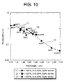
- the relationship between the PL wavelength and the PL intensity was investigated in the combination of Ga x In 1-x As 1-y1-y2 N y1 Sb y2 well layer and a pair of GaNAs barrier layers for an In content of 37% and the nitrogen contents of 0.35% and 0.90%, with the heat treatment temperature being a parameter.
- the results are shown in Fig. 11.
- the optical properties of the GaInAs semiconductor laser devices having an emission wavelength of 1.2 ⁇ m band, wherein In is included at an atomic ratio of 30% or more relative to Group-III elements can be improved remarkably by adding Sb as a constituent element at an atomic ratio of 0.3% to 0.8% relative V-group elements during the epitaxial growth of the GaInAs layer.
- Sb is added at an atomic ratio of 0.2% to 2.5% relative to the V-group elements during the epitaxial growth of the GaInNAs layer.
- a higher nitrogen content may degrade the crystallinity of the semiconductor laser, and thus the practical upper limit of the nitrogen content is preferably below 3% relative to V-group elements.
- GaNAs barrier layers assist for lasing with a lower threshold current at an emission wavelength of 1.3 ⁇ m.
- the GaNAs layer should be made of GaN y As 1-y (y ⁇ 0.05).
- a semiconductor laser device is implemented as a 1.2- ⁇ m band GaInAsSb semiconductor laser device of a facet emission type.
- the SQW active layer structure 20 includes a single well layer made of Ga 0.61 In 0.39 As 0.9968 Sb 0.0032 having a compressive strain of 2.82%, and the thickness of the well layer is 7.3 nm.
- the GaInAsSb well layer is grown under the following conditions in case of gas-source MBE growth:
- the semiconductor laser device of the present embodiment is formed as a ridge waveguide semiconductor laser device by mesa-etching of the above layers to have an active layer width of 3 ⁇ m.
- the semiconductor laser device also includes a p-side ohmix electrode made of metallic layers including Au-Zn or Ti/Pt/Au films on the contact layer 26, and an n-side ohmic electrode made of metallic layers including Au-Ge/Ni/Au films.
- the semiconductor laser device has a cavity length of 200 ⁇ m, and includes a high reflective (HR)-coat having a reflectance of 78% at the front facet and a HR-coat having a reflectance of 95% at the rear facet.
- HR high reflective
- a sample of the semiconductor laser device of the present embodiment was fabricated and subjected to measurements for characteristics of the optical output with respect to injected current after the bonding thereof.
- the results of the measurements were such that the threshold current at 20 degrees C was 6 mA, the characteristic temperature of the threshold current between 20 and 70 degrees C was 256K, and CW emission wavelength was 1.20 ⁇ m at a room temperature.
- the sample had a threshold current which is lowest among the high-strained GaInAs semiconductor laser devices reported heretofore and a characteristic temperature which is significantly higher than those of the conventional ones.
- a semiconductor laser device is implemented as a GaInAsN semiconductor laser device having an emission wavelength of 1.25 to 1.3 ⁇ m band.
- the semiconductor laser device 30 of the present embodiment is similar to the first embodiment except that a SQW active layer structure 32 including a single GaInAsNSb well layer is used in the present embodiment instead of the GaInAsSb SQW structure 20 in the first embodiment.
- the SQW active layer structure 32 includes a single Ga 0.61 In 0.39 As 0.9796 N 0.0044 Sb 0.016 well layer having a thickness of 7.3 nm.
- the GaInNAsSb well layer is grown under the following conditions:
- a sample of the semiconductor laser device of the present embodiment was fabricated and subjected to measurements for characteristics of the optical output with respect to injected current after the bonding thereof.
- the results of the measurements were such that the threshold current at 20 degrees C was 10 mA, the characteristic temperature of the threshold current between 20 and 85 degrees C was 157K, and the CW emission wavelength was 1.26 ⁇ m at a room temperature.
- the sample had a threshold current which is the lowest among the high-strained GaInNAs semiconductor laser devices reported heretofore and a characteristic temperature which is significantly higher than those of the conventional ones.
- the sample had a CW emission wavelength of 1.26 ⁇ m
- a variation of the configuration of the second embodiment provides a semiconductor laser device having an emission wavelength of 1.3 ⁇ m by adjusting the nitrogen content and the Sb content and by additionally using barrier layers each having a composition of GaN y AS 1-y (N ⁇ 0.05).
- the semiconductor laser device of the present invention may be a MQW laser device instead of the SQW laser devices as used in the first and second embodiments.
- the In content may be preferably in the range between 15% and 45% although the In content in the embodiments was exemplified at 39%.
- the GaAs or GaNAs barrier layers as used in the first or second embodiment may be GaInNAs(Sb) or GaInAsP layers, each of which may have a strain.
- the GaAs optical confinement layer having a SCH (Separate Confinement Heterostructure) configuration as used in the embodiments may be replaced by an Al x Ga 1-x As layer having a GRIN (Graded Refractive Index)-SCH configuration.
- the cladding layer may be made of AlGaAs.
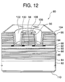
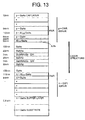
- a semiconductor laser device is implemented as a 1.3- ⁇ m band VCSELs device having a GaInNAsSb/GaNAs active layer structure.
- Each layer of the pair of layers in both the bottom DBR mirror and the top DBR mirror has a thickness corresponding to ⁇ /4n, given ⁇ and n being the emission wavelength of the laser device and the refractive index of the each layer, respectively.
- the pair of layers in the bottom DBR mirror includes a 94-nm-thick n-GaAs layer and a 110-nm-thick n-Al 0.9 Ga 0.1 As layer.
- the pair of layers in the top DBR mirror includes a 94-nm-thick p-GaAs layer and a 110-nm-thick p-Al 0.9 Ga 0.1 As layer.
- the SQW active layer structure 90 includes two wells each including a 7-nm-thick Ga 0.63 In 0.37 N 0.009 As 0.975 Sb 0.016 , and a pair of 20-nm-thick GaN 0.018 As 0.9812 barrier layer.
- the GaInNAsSb well layers were grown under the following conditions:
- Each pair in the top p-type DBR mirror includes a 110-nm-thick Al 0.9 Ga 0.1 As and a 94-nm-thick p-GaAs layer.
- the bottom of the top p-type DBR mirror is implemented by a 20-nm-thick AlAs layer 98 and a 90-nm-thick Al 0.9 Ga 0.1 As layer instead of the 110-nm-thick Al 0.9 Ga 0.1 As layer.
- the bottom layers form a current confinement structure implemented by a non-oxidized area of the AlAs layer 98 which functions as a current injection area 100, and an oxidized area of the AlAs layer 98 wherein Al in the AlAs layer 98 is oxidized.
- the top DBR mirror 94 is configured by a photolithographic etching technique to form a annular groove 102 having a width of, for example, 50 ⁇ m.
- the annular groove 102 defines a cylindrical mesa post having a diameter of 20 ⁇ m.
- a SiN x film 104 is formed as an insulation layer for the entire layer structure including the annular groove 102 and except for the top of the mesa post.
- An annular p-side electrode 106 is formed inside the SiNx film 104 in contact with the p-GaAs cap layer 96.
- An electrode pad 108 made of Ti/Pt/Au films is formed on the annular p-side electrode 106 and the SiNx film 104.
- the bottom of the GaAs substrate 82 is polished for allowing the GaAs substrate 82 to have a thickness of 100 ⁇ m.
- An n-side electrode 110 is formed on the bottom surface of the GaAs substrate 82.
- the semiconductor laser device lased with a CW mode at a threshold current of 2 mA and at a temperature of 100 degrees C or above.
- the semiconductor laser devices had emission wavelengths of 1200 nm and 1250 to 1300 nm.
- the present invention can be applied to a semiconductor laser device or VCSEL having emission wavelengths of 980 nm, 1480 nm, 1550 nm, 1650 nm etc. by modifying the nitrogen content and the Sb content.
Landscapes
- Physics & Mathematics (AREA)
- Optics & Photonics (AREA)
- Condensed Matter Physics & Semiconductors (AREA)
- General Physics & Mathematics (AREA)
- Electromagnetism (AREA)
- Chemical & Material Sciences (AREA)
- Engineering & Computer Science (AREA)
- Nanotechnology (AREA)
- Life Sciences & Earth Sciences (AREA)
- Biophysics (AREA)
- Crystallography & Structural Chemistry (AREA)
- Semiconductor Lasers (AREA)
Abstract
Description
Although a GaInAsP semiconductor laser device formed on an InP substrate is conventionally developed as a semiconductor laser device having an emission wavelength of 1.3 ìm band, it has been a problem that the semiconductor materials used in the GaInAsP laser device has a poor characteristic temperature of the threshold current as low as 50K to 70K, which degrades the temperature characteristics of the laser device. In order to dispose a semiconductor laser device in each of households as a light source, it is desired that the semiconductor laser module have a longer wavelength band and a superior temperature characteristic without using a cooling device, and also can be manufactured at a lower cost.
Thus, a variety of semiconductor laser devices having improved temperature characteristics and longer emission wavelengths have been developed. It is reported in "Jpn.J.Appl.Phys., vol.35(1996)", pp.1273-1275 by M. Kondow et al. that one of the semiconductor laser devices thus developed may have a temperature characteristic as high as about 180K. Also it is assured therein by an experiments that a prototype semiconductor laser device achieved a higher temperature characteristic around 130K to 270K.
It is another object of the present invention to provide a method for manufacturing such a GaInNAs semiconductor device.
The present inventor noticed the effectiveness of addition of Sb in a minute amount of about 0.2% to 2.5% with respect to the amount of V-group elements together with addition of a Group-III element during the growth of the high strained layer, without disposing the surfactant on the underlying layer before growing the high-strained layer.
More specifically, a GalnAsSb layer is formed in a 1.2-ìm band GaInAs semiconductor laser device, whereas a GaInNAsSb layer is formed in a 1.3-ìm band GaInNAs semiconductor laser device. The experiments as detailed below and conducted by the inventor revealed the superiority of this technique to the conventional technique.
A GaIn0.39As SQW layer has a higher compressive strain as high as 2.8%. The design thickness of the SQW layer structure is set at 7.3 nm, wherein the relationship between the critical thickness and the In content is calculated to obtain 4 nm for the critical thickness based on the theory presented by J.W.Matthews and A.E.Blakeslee for the GaInAs/GaAs semiconductor laser device.
In these experiments, Sb is added only to a GaIn0.39As SQW layer to form a GaInAsSb SQW layer. By changing the Sb flux (Torr) as a parameter, the photoluminescence (PL) dependency of the Sb flux was investigated. The results are shown in Fig. 5. The term "amount of Sb flux" or simply "Sb flux" as used herein means the intensity of the molecular beam of Sb incident onto the substrate and evaluated in terms of the partial pressure at the surface of the substrate.
The growth conditions of the GaInAsSb layer in the experiments are as follows:
The PL wavelength indicated relatively good coincidence to the calculation up to a Sb flux of 2x10⁻⁶Torr.
Figs. 8A and 8B respectively show the TEM image photography of GaInNAsSb layers grown with the addition of Sb at amounts of Sb flux of 2x10⁻⁷ Torr and 1x10⁻⁶ Torr, respectively.
In the third experiments, although the PL wavelength after the heat treatment is 1.24 ìm for a nitrogen content of 0.44% and a Sb flux of 1x10⁻⁶ Torr, the emission wavelength is desirable to be increased up to 1.35 ìm in consideration that WDM (wavelength division multiplexing) system is expected to develop into a 1.3 ìm band wavelength. In such a case, the nitrogen content should be increased up to around 1.5% depending on the In content.
| temperature of heat treatment | wavelength | PL intensity |
| degrees C | ìm | (a.u.) |
| 500 | 1.223 | 0.69 |
| 550 | 1.212 | 0.99 |
| 600 | 1.192 | 1.7 |
| 650 | 1.181 | 1.58 |
| 700 |
| temperature of heat treatment | wavelength | PL intensity |
| degrees C | ìm | (a.u.) |
| 500 - | 1.263 | 0.43 |
| 550 | 1.252 | 0.47 |
| 600 | 1.232 | 0.9 |
| 650 | 1.211 | 0.81 |
| 700 |
| temperature of heat treatment | wavelength | PL intensity |
| degrees C | ìm | (a.u.) |
| 500 | 1.338 | 0.04 |
| 550 | 1.312 | 0.06 |
| 600 | 1.280 | 0.17 |
| 650 | 1.266 | 0.28 |
| 700 | 1.248 | 0.56 |
| temperature of heat treatment | wavelength | PL intensity |
| degrees C | ìm | (a.u.) |
| 500 | 1.255 | 0.54 |
| 550 - | 1.249 | 0.54 |
| 600 | 1.230 | 0.74 |
| 650 | 1.218 | 0.49 |
| 700 |
| temperature of heat treatment | wavelength | PL intensity |
| degrees C | ìm | (a.u.) |
| 500 | 1.286 | 0.28 |
| 550 | 1.281 | 0.20 |
| 600 | 1.257 | 0.44 |
| 650 | 1.238 | 0.54 |
| 700 |
For example, the relationship between the PL wavelength and the PL intensity for the case of an In content of 37% and a nitrogen flow rate of 0.05 sccm is such that shown by the graph (1) wherein the wavelength of the as-grown layer is 1.222 ìm whereas the wavelengths of the epitaxial layers subjected to the heat treatments at 550 degrees C and 650 degrees C are 1.21 ìm and 1.18 ìm, respectively.
| temperature of heat treatment | wavelength | PL intensity |
| degrees C | ìm | (a.u.) |
| 500 | 1.243 | 0.52 |
| 550 | 1.240 | 0.96 |
| 600 | 1.219 | 2.2 |
| 650 | 1.206 | 2.7 |
| 700 | 1.198 | 5.5 |
| temperature of heat treatment | wavelength | PL intensity |
| degrees C | ìm | (a.u.) |
| 500 | 1.279 | 0.24 |
| 550 | 1.274 | 0.45 |
| 600 | 1.253 | 1.4 |
| 650 | 1.234 | 2.0 |
| 700 | 1.226 | 2.4 |
| temperature of heat treatment | wavelength | PL intensity |
| degrees C | ìm | (a.u.) |
| 500 | 1.348 | 0.03 |
| 550 | 1.336 | 0.29 |
| 600 | 1.328 | 0.38 |
| 650 | 1.296 | 1.23 |
| 700 | 1.262 | 1.83 |
| temperature of heat treatment | wavelength | PL intensity |
| degrees C | ìm | (a.u.) |
| 500 | ||
| 550 | 1.240 | 0.09 |
| 600 | 1.226 | 3.7 |
| 650 | 1.221 | 3.9 |
| 700 |
Although the PL intensity of the as-grown epitaxial layers including a pair of GaNAs barrier layers is lower, the PL intensity increases sharply after the heat treatment at 650°C or above.
Thus, a laser structure including SQW active layer structure having Ga0.63In0.37N0.009As0.975Sb0.016/GaN0.018As0.982 layers was fabricated as a broad contact laser, which exhibited a excellent lower threshold current as low as 570 A/cm2 for a cavity length of 900 ìm.
The GaInAsSb well layer is grown under the following conditions in case of gas-source MBE growth:
Although the sample had a CW emission wavelength of 1.26 ìm, a variation of the configuration of the second embodiment provides a semiconductor laser device having an emission wavelength of 1.3 ìm by adjusting the nitrogen content and the Sb content and by additionally using barrier layers each having a composition of GaNyAS1-y (N<0.05). The semiconductor laser device of the present invention may be a MQW laser device instead of the SQW laser devices as used in the first and second embodiments. The In content may be preferably in the range between 15% and 45% although the In content in the embodiments was exemplified at 39%.
Each layer of the pair of layers in both the bottom DBR mirror and the top DBR mirror has a thickness corresponding to λ/4n, given λ and n being the emission wavelength of the laser device and the refractive index of the each layer, respectively.
More specifically, the pair of layers in the bottom DBR mirror includes a 94-nm-thick n-GaAs layer and a 110-nm-thick n-Al0.9Ga0.1As layer. The pair of layers in the top DBR mirror includes a 94-nm-thick p-GaAs layer and a 110-nm-thick p-Al0.9Ga0.1As layer.
The bottom layers form a current confinement structure implemented by a non-oxidized area of the AlAs
Claims (28)
- A semiconductor laser comprising:a substrate;a QW active layer structure formed over said substrate, wherein said QW active layer structure includes at least one QW active layer comprising GaxIn1-xAsySb1-y, and wherein 0.3 ≦ 1-x and wherein 0.003 ≦ 1-y ≦ 0.008.
- The semiconductor laser of Claim 1, wherein said substrate comprises GaAs.
- The semiconductor laser of Claim 1, wherein said laser emits laser light having a wavelength of at least about 1.18 ìm.
- The semiconductor laser of Claim 3 comprising at least two active layers of GaxIn1-xAsySb1-y.
- The semiconductor laser of Claim 1, wherein said semiconductor laser comprises a VCSEL.
- The semiconductor laser of Claim 1, wherein said semiconductor laser comprises an edge emitting laser.
- A method of making a QW active layer for a semiconductor laser comprising depositing a layer of Ga, In, As, and Sb onto a GaAs substrate, wherein said depositing is performed with a partial pressure of Sb that is sufficient to form an active layer of about 0.3% to about 0.8% in atomic ratio of Sb relative to the amount of As.
- A method of making a QW active layer for a semiconductor laser comprising depositing a layer of Ga, In, N, As, and Sb onto a GaAs substrate, wherein said depositing is performed with a partial pressure of Sb that is sufficient to form an active layer of about 0.2% to about 6% in atomic ratio of Sb relative to the combined amounts of As and N.
- The method of Claim 8, wherein said active layer is deposited between barrier layers of GaNzAs1-z.
- The method of Claim 9, additionally comprising heat treating said active layer after deposition at a temperature of about 675 to 725 degrees C.
- A semiconductor laser comprising:a substrate;one or more QW active layers formed over said substrate, wherein at least one of said one or more QW active layers comprises GaxIn1-xAs1-y1-y2Ny1Sby2, wherein 0.3 ≦ 1-x, wherein 0 < y1 < 0.03, and wherein 0.002 ≦ y2 ≦ 0.06.
- The semiconductor laser of Claim 11, wherein said substrate comprises GaAs.
- The semiconductor laser of Claim 11, wherein said laser emits laser light having a wavelength of at least about 1.24 ìm.
- The semiconductor laser of Claim 13 comprising at least two active layers of GaxIn1-xAs1-y1-y2Ny1Sby2.
- The semiconductor laser of Claim 11, wherein said semiconductor laser comprises a VCSEL.
- The semiconductor laser of Claim 11, wherein said semiconductor laser comprises an edge emitting laser.
- The semiconductor laser of Claim 11, wherein at least one of said active layers is placed between barrier layers of GaNzAs1-z.
- The semiconductor laser of Claim 17, wherein 0 ≦ z ≦ 0.05.
- A semiconductor laser comprising:an active layer comprising co-deposited Ga, As, In, N, and Sb; and a pair of barrier layers, one on each side of said active layer, said barrier layers comprising Ga, As, and N.
- The semiconductor laser of Claim 19, wherein said substrate comprises GaAs.
- The semiconductor laser of Claim 19, wherein said semiconductor laser has a lasing wavelength of at least about 1.24 ìm.
- A method of making a semiconductor laser comprising:depositing a first barrier layer of GaNzAs1-z onto a substrate;depositing an active layer of GaxIn1-xAs1-y1-y2Ny1Sby2 over said first barrier layer; and depositing a second barrier layer of GaNzAs1-z over said active layer.
- The method of Claim 22, wherein said substrate comprises GaAs.
- The method of Claim 22, wherein 0.3 ≦ 1-x, wherein 0 ≦y1 ≦ 0.03, and wherein 0.002 ≦ y2 ≦ 0.06.
- The method of Claim 22 wherein 0 < z ≦ 0.05.
- The method of Claim 22, additionally comprising heat treating said layers at a temperature of about 675 to about 725 degrees C.
- A method for manufacturing a semiconductor laser device comprising:forming a laser structure by depositing one or more QW active layers over a substrate, wherein at least one of said one or more QW active layers comprises GaxIn1-xAs1-y1-y2Ny1Sby2, wherein 0.3 ≤ 1-x, wherein 0 ≦ y1 ≦ 0.007, and wherein 0.002 ≦ y2 ≦ 0.06, and heat treating said laser structure, after growth of said one or more layers at a temperature of about 570 to 630 degrees C.
- A method for manufacturing a semiconductor laser device comprising:forming a laser structure by depositing one or more QW active layers over a substrate, wherein at least one of said one or more QW active layers comprises GaxIn1-xAs1-y1-y2Ny1Sby2, wherein 0.3 ≦ 1-x, wherein 0.007 ≦ y1 ≦ 0.03, and wherein 0.002 ≦ y2 ≦ 0.06, and heat treating said laser structure, after growth of said one or more layers at a temperature of about 670 to 730 degrees C.
Applications Claiming Priority (4)
| Application Number | Priority Date | Filing Date | Title |
|---|---|---|---|
| JP2000230553 | 2000-07-31 | ||
| JP2000230553 | 2000-07-31 | ||
| JP2001124300 | 2001-04-23 | ||
| JP2001124300A JP3735047B2 (en) | 2000-07-31 | 2001-04-23 | Semiconductor laser device and manufacturing method thereof |
Publications (3)
| Publication Number | Publication Date |
|---|---|
| EP1182756A2 true EP1182756A2 (en) | 2002-02-27 |
| EP1182756A3 EP1182756A3 (en) | 2003-07-16 |
| EP1182756B1 EP1182756B1 (en) | 2006-09-20 |
Family
ID=26597005
Family Applications (1)
| Application Number | Title | Priority Date | Filing Date |
|---|---|---|---|
| EP01118280A Expired - Lifetime EP1182756B1 (en) | 2000-07-31 | 2001-07-30 | Semiconductor laser device having lower threshold current |
Country Status (5)
| Country | Link |
|---|---|
| US (2) | US6912236B2 (en) |
| EP (1) | EP1182756B1 (en) |
| JP (1) | JP3735047B2 (en) |
| CA (1) | CA2354420A1 (en) |
| DE (1) | DE60123185T2 (en) |
Cited By (5)
| Publication number | Priority date | Publication date | Assignee | Title |
|---|---|---|---|---|
| WO2003058770A3 (en) * | 2001-12-20 | 2004-02-12 | Honeywell Int Inc | Vertical cavity surface emitting laser including indium and nitrogen in the active region |
| WO2003058771A3 (en) * | 2001-12-27 | 2004-03-18 | Honeywell Int Inc | Vertical cavity surface emitting laser including indium and antimony in the active region |
| WO2004070900A1 (en) * | 2003-01-27 | 2004-08-19 | Finisar Corporation | System and methods using migration enhanced epitaxy for flattening active layers and the mechanical stabilization of quantum wells associated with vertical cavity surface emitting lasers |
| EP1349246A3 (en) * | 2002-03-25 | 2005-06-29 | Agilent Technologies, Inc. | Asymmetric InGaAsN vertical cavity surface emitting lasers |
| US8168456B2 (en) | 2004-10-01 | 2012-05-01 | Finisar Corporation | Vertical cavity surface emitting laser with undoped top mirror |
Families Citing this family (30)
| Publication number | Priority date | Publication date | Assignee | Title |
|---|---|---|---|---|
| US7257143B2 (en) * | 1998-12-21 | 2007-08-14 | Finisar Corporation | Multicomponent barrier layers in quantum well active regions to enhance confinement and speed |
| US7058112B2 (en) * | 2001-12-27 | 2006-06-06 | Finisar Corporation | Indium free vertical cavity surface emitting laser |
| US7435660B2 (en) | 1998-12-21 | 2008-10-14 | Finisar Corporation | Migration enhanced epitaxy fabrication of active regions having quantum wells |
| US7286585B2 (en) * | 1998-12-21 | 2007-10-23 | Finisar Corporation | Low temperature grown layers with migration enhanced epitaxy adjacent to an InGaAsN(Sb) based active region |
| US7167495B2 (en) * | 1998-12-21 | 2007-01-23 | Finisar Corporation | Use of GaAs extended barrier layers between active regions containing nitrogen and AlGaAs confining layers |
| JP2003017812A (en) * | 2001-04-25 | 2003-01-17 | Furukawa Electric Co Ltd:The | Semiconductor laser device |
| JP4025227B2 (en) * | 2002-03-29 | 2007-12-19 | 株式会社東芝 | Semiconductor laminated substrate and optical semiconductor element |
| US7656924B2 (en) | 2002-04-05 | 2010-02-02 | The Furukawa Electric Co., Ltd. | Surface emitting laser, and transceiver, optical transceiver, and optical communication system employing the surface emitting laser |
| JP3966067B2 (en) * | 2002-04-26 | 2007-08-29 | 富士ゼロックス株式会社 | Surface emitting semiconductor laser device and method for manufacturing the same |
| JP4615179B2 (en) * | 2002-06-27 | 2011-01-19 | 古河電気工業株式会社 | Semiconductor laser device, semiconductor laser module, and optical fiber amplifier |
| JP2004063969A (en) * | 2002-07-31 | 2004-02-26 | Victor Co Of Japan Ltd | Surface-emitting laser |
| US6927412B2 (en) | 2002-11-21 | 2005-08-09 | Ricoh Company, Ltd. | Semiconductor light emitter |
| DE10331586B4 (en) * | 2003-07-09 | 2006-08-31 | Universität Kassel | Microlaser device and method for its production |
| GB2407700A (en) * | 2003-10-28 | 2005-05-04 | Sharp Kk | MBE growth of nitride semiconductor lasers |
| JP4579526B2 (en) * | 2003-11-10 | 2010-11-10 | 古河電気工業株式会社 | Surface emitting laser |
| WO2005086243A1 (en) * | 2004-03-08 | 2005-09-15 | Showa Denko K.K. | Pn junction type croup iii nitride semiconductor light-emitting device |
| JP4639649B2 (en) * | 2004-03-26 | 2011-02-23 | 住友電気工業株式会社 | Method for growing III-V compound semiconductor layer, epitaxial wafer, and semiconductor device |
| JP4643184B2 (en) * | 2004-06-29 | 2011-03-02 | シャープ株式会社 | Semiconductor device, system, and method of manufacturing semiconductor device |
| CA2581614A1 (en) | 2004-10-01 | 2006-04-13 | Finisar Corporation | Vertical cavity surface emitting laser having multiple top-side contacts |
| US7720323B2 (en) * | 2004-12-20 | 2010-05-18 | Schlumberger Technology Corporation | High-temperature downhole devices |
| JP4575173B2 (en) * | 2005-01-07 | 2010-11-04 | 日本電信電話株式会社 | Manufacturing method of quantum well structure |
| JP4662345B2 (en) * | 2005-03-28 | 2011-03-30 | 日本電信電話株式会社 | Multiple strain quantum well structure and manufacturing method thereof |
| JP2007251089A (en) * | 2006-03-20 | 2007-09-27 | Nippon Telegr & Teleph Corp <Ntt> | Manufacturing method of semiconductor multilayer structure and manufacturing method of semiconductor quantum dot structure |
| JP5397929B2 (en) * | 2008-01-22 | 2014-01-22 | 独立行政法人情報通信研究機構 | Semiconductor optical device, semiconductor device for optical communication, and manufacturing method thereof |
| JP5274038B2 (en) * | 2008-02-06 | 2013-08-28 | キヤノン株式会社 | Manufacturing method of vertical cavity surface emitting laser and manufacturing method of laser array |
| JP4963301B2 (en) * | 2008-05-15 | 2012-06-27 | シャープ株式会社 | Manufacturing method of nitride semiconductor light emitting device |
| JP2012156562A (en) * | 2012-05-21 | 2012-08-16 | Nec Corp | Surface emitting laser |
| US10043941B1 (en) | 2017-01-31 | 2018-08-07 | International Business Machines Corporation | Light emitting diode having improved quantum efficiency at low injection current |
| CN110600996B (en) * | 2019-09-26 | 2024-05-14 | 苏州矩阵光电有限公司 | Quantum well layer structure, semiconductor laser and preparation method |
| WO2021133827A2 (en) * | 2019-12-24 | 2021-07-01 | Array Photonics, Inc. | Stacked semiconductor lasers with controlled spectral emission |
Family Cites Families (15)
| Publication number | Priority date | Publication date | Assignee | Title |
|---|---|---|---|---|
| US5383211A (en) * | 1993-11-02 | 1995-01-17 | Xerox Corporation | TM-polarized laser emitter using III-V alloy with nitrogen |
| US5689123A (en) | 1994-04-07 | 1997-11-18 | Sdl, Inc. | III-V aresenide-nitride semiconductor materials and devices |
| US5451552A (en) * | 1994-05-13 | 1995-09-19 | Hughes Aircraft Company | Method for improvement of optical quality and reduction of background doping in gainSB/INAS superlattices |
| US5719894A (en) | 1996-09-25 | 1998-02-17 | Picolight Incorporated | Extended wavelength strained layer lasers having nitrogen disposed therein |
| US5825796A (en) * | 1996-09-25 | 1998-10-20 | Picolight Incorporated | Extended wavelength strained layer lasers having strain compensated layers |
| US5719895A (en) | 1996-09-25 | 1998-02-17 | Picolight Incorporated | Extended wavelength strained layer lasers having short period superlattices |
| JP3854693B2 (en) * | 1996-09-30 | 2006-12-06 | キヤノン株式会社 | Manufacturing method of semiconductor laser |
| US6330263B1 (en) * | 1998-05-06 | 2001-12-11 | Sarnoff Corporation | Laser diode having separated, highly-strained quantum wells |
| DE69921189T2 (en) * | 1998-12-03 | 2006-02-02 | Arizona Board Of Regents, Tempe | CONNECTING SEMICONDUCTOR STRUCTURE FOR OPTOELECTRONIC COMPONENTS |
| US6603784B1 (en) | 1998-12-21 | 2003-08-05 | Honeywell International Inc. | Mechanical stabilization of lattice mismatched quantum wells |
| US7095770B2 (en) * | 2001-12-20 | 2006-08-22 | Finisar Corporation | Vertical cavity surface emitting laser including indium, antimony and nitrogen in the active region |
| US6424669B1 (en) * | 1999-10-29 | 2002-07-23 | E20 Communications, Inc. | Integrated optically pumped vertical cavity surface emitting laser |
| EP1228557A2 (en) | 1999-11-01 | 2002-08-07 | Arizona Board of Regents | Long wavelength pseudomorphic inganpassb type-i and type-ii active layers for the gas material system |
| US6859474B1 (en) * | 1999-11-01 | 2005-02-22 | Arizona Board Of Regents | Long wavelength pseudomorphic InGaNPAsSb type-I and type-II active layers for the gaas material system |
| US20020075920A1 (en) * | 2000-12-15 | 2002-06-20 | Sylvia Spruytte | Laser diode device with nitrogen incorporating barrier |
-
2001
- 2001-04-23 JP JP2001124300A patent/JP3735047B2/en not_active Expired - Fee Related
- 2001-07-30 DE DE60123185T patent/DE60123185T2/en not_active Expired - Lifetime
- 2001-07-30 EP EP01118280A patent/EP1182756B1/en not_active Expired - Lifetime
- 2001-07-30 US US09/918,018 patent/US6912236B2/en not_active Expired - Fee Related
- 2001-07-30 CA CA002354420A patent/CA2354420A1/en not_active Abandoned
-
2005
- 2005-04-18 US US11/107,871 patent/US20050180485A1/en not_active Abandoned
Cited By (7)
| Publication number | Priority date | Publication date | Assignee | Title |
|---|---|---|---|---|
| WO2003058770A3 (en) * | 2001-12-20 | 2004-02-12 | Honeywell Int Inc | Vertical cavity surface emitting laser including indium and nitrogen in the active region |
| US7408964B2 (en) | 2001-12-20 | 2008-08-05 | Finisar Corporation | Vertical cavity surface emitting laser including indium and nitrogen in the active region |
| WO2003058771A3 (en) * | 2001-12-27 | 2004-03-18 | Honeywell Int Inc | Vertical cavity surface emitting laser including indium and antimony in the active region |
| US6975660B2 (en) | 2001-12-27 | 2005-12-13 | Finisar Corporation | Vertical cavity surface emitting laser including indium and antimony in the active region |
| EP1349246A3 (en) * | 2002-03-25 | 2005-06-29 | Agilent Technologies, Inc. | Asymmetric InGaAsN vertical cavity surface emitting lasers |
| WO2004070900A1 (en) * | 2003-01-27 | 2004-08-19 | Finisar Corporation | System and methods using migration enhanced epitaxy for flattening active layers and the mechanical stabilization of quantum wells associated with vertical cavity surface emitting lasers |
| US8168456B2 (en) | 2004-10-01 | 2012-05-01 | Finisar Corporation | Vertical cavity surface emitting laser with undoped top mirror |
Also Published As
| Publication number | Publication date |
|---|---|
| DE60123185T2 (en) | 2007-10-11 |
| DE60123185D1 (en) | 2006-11-02 |
| CA2354420A1 (en) | 2002-01-31 |
| US6912236B2 (en) | 2005-06-28 |
| US20050180485A1 (en) | 2005-08-18 |
| US20020034203A1 (en) | 2002-03-21 |
| EP1182756A3 (en) | 2003-07-16 |
| JP3735047B2 (en) | 2006-01-11 |
| JP2002118329A (en) | 2002-04-19 |
| EP1182756B1 (en) | 2006-09-20 |
Similar Documents
| Publication | Publication Date | Title |
|---|---|---|
| US6912236B2 (en) | Semiconductor laser device having lower threshold current | |
| US6207973B1 (en) | Light emitting devices with layered III-V semiconductor structures | |
| US6782021B2 (en) | Quantum dot vertical cavity surface emitting laser | |
| EP1145395B1 (en) | Compound semiconductor structures for optoelectronic devices | |
| JP4663964B2 (en) | Long wavelength photonics device comprising a GaAsSb quantum well layer | |
| US6657233B2 (en) | Light emitting devices with layered III-V semiconductor structures, and modules and systems for computer, network and optical communication, using such device | |
| US20020131462A1 (en) | Intracavity contacted long wavelength VCSELs with buried antimony layers | |
| US20040161006A1 (en) | Method and apparatus for improving wavelength stability for InGaAsN devices | |
| JP3189791B2 (en) | Semiconductor laser | |
| US6858863B2 (en) | Semiconductor laser device having a high characteristic temperature | |
| US6931044B2 (en) | Method and apparatus for improving temperature performance for GaAsSb/GaAs devices | |
| US20020014674A1 (en) | Light emitting device and light emitting device module | |
| Taniguchi et al. | 25-W 915-nm lasers with window structure fabricated by impurity-free vacancy disordering (IFVD) | |
| US20060193361A1 (en) | Vertical cavity surface emitting laser device having a higher optical output power | |
| JP4084506B2 (en) | Manufacturing method of semiconductor light emitting device | |
| US7459719B2 (en) | Superlattice optical semiconductor device where each barrier layer has high content of group III elements in center portion and low content near well layer | |
| US20020167985A1 (en) | Surface emitting semiconductor laser device | |
| US20050243889A1 (en) | Digital alloy oxidation layers | |
| US20050243881A1 (en) | InAlAs having enhanced oxidation rate grown under very low V/III ratio | |
| JP4957355B2 (en) | Semiconductor light emitting device | |
| Watanabe et al. | High-temperature operation (70/spl deg/C, 50 mW) of 660-nm-band InGaAlP Zn-diffused window lasers fabricated using highly Zn-doped GaAs layers | |
| Lai et al. | MBE-grown 1.3 micron InGaAsN/GaAs double QW VCSELs with very low-threshold current density under room temperature CW operation | |
| Shimizu et al. | 1.26/spl mu/m GaInNAsSb-SQW lasers grown by gas-source MBE | |
| JP2008098682A (en) | Semiconductor light emitting device | |
| Tränkle et al. | Visible (Red) Vertical-Cavity Surface-Emitting Lasers |
Legal Events
| Date | Code | Title | Description |
|---|---|---|---|
| PUAI | Public reference made under article 153(3) epc to a published international application that has entered the european phase |
Free format text: ORIGINAL CODE: 0009012 |
|
| AK | Designated contracting states |
Kind code of ref document: A2 Designated state(s): AT BE CH CY DE DK ES FI FR GB GR IE IT LI LU MC NL PT SE TR |
|
| AX | Request for extension of the european patent |
Free format text: AL;LT;LV;MK;RO;SI |
|
| PUAL | Search report despatched |
Free format text: ORIGINAL CODE: 0009013 |
|
| AK | Designated contracting states |
Designated state(s): AT BE CH CY DE DK ES FI FR GB GR IE IT LI LU MC NL PT SE TR |
|
| AX | Request for extension of the european patent |
Extension state: AL LT LV MK RO SI |
|
| 17P | Request for examination filed |
Effective date: 20031218 |
|
| AKX | Designation fees paid |
Designated state(s): DE FR GB |
|
| 17Q | First examination report despatched |
Effective date: 20041208 |
|
| GRAP | Despatch of communication of intention to grant a patent |
Free format text: ORIGINAL CODE: EPIDOSNIGR1 |
|
| GRAS | Grant fee paid |
Free format text: ORIGINAL CODE: EPIDOSNIGR3 |
|
| GRAA | (expected) grant |
Free format text: ORIGINAL CODE: 0009210 |
|
| AK | Designated contracting states |
Kind code of ref document: B1 Designated state(s): DE FR GB |
|
| REG | Reference to a national code |
Ref country code: GB Ref legal event code: FG4D |
|
| REF | Corresponds to: |
Ref document number: 60123185 Country of ref document: DE Date of ref document: 20061102 Kind code of ref document: P |
|
| EN | Fr: translation not filed | ||
| PLBE | No opposition filed within time limit |
Free format text: ORIGINAL CODE: 0009261 |
|
| STAA | Information on the status of an ep patent application or granted ep patent |
Free format text: STATUS: NO OPPOSITION FILED WITHIN TIME LIMIT |
|
| 26N | No opposition filed |
Effective date: 20070621 |
|
| PG25 | Lapsed in a contracting state [announced via postgrant information from national office to epo] |
Ref country code: FR Free format text: LAPSE BECAUSE OF FAILURE TO SUBMIT A TRANSLATION OF THE DESCRIPTION OR TO PAY THE FEE WITHIN THE PRESCRIBED TIME-LIMIT Effective date: 20070518 |
|
| PG25 | Lapsed in a contracting state [announced via postgrant information from national office to epo] |
Ref country code: FR Free format text: LAPSE BECAUSE OF FAILURE TO SUBMIT A TRANSLATION OF THE DESCRIPTION OR TO PAY THE FEE WITHIN THE PRESCRIBED TIME-LIMIT Effective date: 20060920 |
|
| PGFP | Annual fee paid to national office [announced via postgrant information from national office to epo] |
Ref country code: DE Payment date: 20100728 Year of fee payment: 10 |
|
| PGFP | Annual fee paid to national office [announced via postgrant information from national office to epo] |
Ref country code: GB Payment date: 20100728 Year of fee payment: 10 |
|
| GBPC | Gb: european patent ceased through non-payment of renewal fee |
Effective date: 20110730 |
|
| PG25 | Lapsed in a contracting state [announced via postgrant information from national office to epo] |
Ref country code: DE Free format text: LAPSE BECAUSE OF FAILURE TO SUBMIT A TRANSLATION OF THE DESCRIPTION OR TO PAY THE FEE WITHIN THE PRESCRIBED TIME-LIMIT Effective date: 20120201 |
|
| REG | Reference to a national code |
Ref country code: DE Ref legal event code: R119 Ref document number: 60123185 Country of ref document: DE Effective date: 20120201 |
|
| PG25 | Lapsed in a contracting state [announced via postgrant information from national office to epo] |
Ref country code: GB Free format text: LAPSE BECAUSE OF NON-PAYMENT OF DUE FEES Effective date: 20110730 |