EP1182665A2 - MRAM with an effective noise countermeasure - Google Patents
MRAM with an effective noise countermeasure Download PDFInfo
- Publication number
- EP1182665A2 EP1182665A2 EP01119925A EP01119925A EP1182665A2 EP 1182665 A2 EP1182665 A2 EP 1182665A2 EP 01119925 A EP01119925 A EP 01119925A EP 01119925 A EP01119925 A EP 01119925A EP 1182665 A2 EP1182665 A2 EP 1182665A2
- Authority
- EP
- European Patent Office
- Prior art keywords
- magnetic
- magnetic material
- frequency current
- device portion
- mram
- Prior art date
- Legal status (The legal status is an assumption and is not a legal conclusion. Google has not performed a legal analysis and makes no representation as to the accuracy of the status listed.)
- Granted
Links
Images


Classifications
-
- G—PHYSICS
- G11—INFORMATION STORAGE
- G11C—STATIC STORES
- G11C11/00—Digital stores characterised by the use of particular electric or magnetic storage elements; Storage elements therefor
- G11C11/02—Digital stores characterised by the use of particular electric or magnetic storage elements; Storage elements therefor using magnetic elements
- G11C11/14—Digital stores characterised by the use of particular electric or magnetic storage elements; Storage elements therefor using magnetic elements using thin-film elements
- G11C11/15—Digital stores characterised by the use of particular electric or magnetic storage elements; Storage elements therefor using magnetic elements using thin-film elements using multiple magnetic layers
-
- H—ELECTRICITY
- H10—SEMICONDUCTOR DEVICES; ELECTRIC SOLID-STATE DEVICES NOT OTHERWISE PROVIDED FOR
- H10D—INORGANIC ELECTRIC SEMICONDUCTOR DEVICES
- H10D84/00—Integrated devices formed in or on semiconductor substrates that comprise only semiconducting layers, e.g. on Si wafers or on GaAs-on-Si wafers
-
- B—PERFORMING OPERATIONS; TRANSPORTING
- B82—NANOTECHNOLOGY
- B82Y—SPECIFIC USES OR APPLICATIONS OF NANOSTRUCTURES; MEASUREMENT OR ANALYSIS OF NANOSTRUCTURES; MANUFACTURE OR TREATMENT OF NANOSTRUCTURES
- B82Y25/00—Nanomagnetism, e.g. magnetoimpedance, anisotropic magnetoresistance, giant magnetoresistance or tunneling magnetoresistance
-
- G—PHYSICS
- G11—INFORMATION STORAGE
- G11C—STATIC STORES
- G11C11/00—Digital stores characterised by the use of particular electric or magnetic storage elements; Storage elements therefor
- G11C11/02—Digital stores characterised by the use of particular electric or magnetic storage elements; Storage elements therefor using magnetic elements
- G11C11/16—Digital stores characterised by the use of particular electric or magnetic storage elements; Storage elements therefor using magnetic elements using elements in which the storage effect is based on magnetic spin effect
-
- H—ELECTRICITY
- H01—ELECTRIC ELEMENTS
- H01F—MAGNETS; INDUCTANCES; TRANSFORMERS; SELECTION OF MATERIALS FOR THEIR MAGNETIC PROPERTIES
- H01F10/00—Thin magnetic films, e.g. of one-domain structure
- H01F10/32—Spin-exchange-coupled multilayers, e.g. nanostructured superlattices
- H01F10/3227—Exchange coupling via one or more magnetisable ultrathin or granular films
-
- H—ELECTRICITY
- H10—SEMICONDUCTOR DEVICES; ELECTRIC SOLID-STATE DEVICES NOT OTHERWISE PROVIDED FOR
- H10W—GENERIC PACKAGES, INTERCONNECTIONS, CONNECTORS OR OTHER CONSTRUCTIONAL DETAILS OF DEVICES COVERED BY CLASS H10
- H10W42/00—Arrangements for protection of devices
- H10W42/20—Arrangements for protection of devices protecting against electromagnetic or particle radiation, e.g. light, X-rays, gamma-rays or electrons
-
- H—ELECTRICITY
- H10—SEMICONDUCTOR DEVICES; ELECTRIC SOLID-STATE DEVICES NOT OTHERWISE PROVIDED FOR
- H10W—GENERIC PACKAGES, INTERCONNECTIONS, CONNECTORS OR OTHER CONSTRUCTIONAL DETAILS OF DEVICES COVERED BY CLASS H10
- H10W42/00—Arrangements for protection of devices
- H10W42/20—Arrangements for protection of devices protecting against electromagnetic or particle radiation, e.g. light, X-rays, gamma-rays or electrons
- H10W42/281—Arrangements for protection of devices protecting against electromagnetic or particle radiation, e.g. light, X-rays, gamma-rays or electrons characterised by their materials
- H10W42/287—Arrangements for protection of devices protecting against electromagnetic or particle radiation, e.g. light, X-rays, gamma-rays or electrons characterised by their materials materials for magnetic shielding, e.g. ferromagnetic materials
-
- H—ELECTRICITY
- H10—SEMICONDUCTOR DEVICES; ELECTRIC SOLID-STATE DEVICES NOT OTHERWISE PROVIDED FOR
- H10W—GENERIC PACKAGES, INTERCONNECTIONS, CONNECTORS OR OTHER CONSTRUCTIONAL DETAILS OF DEVICES COVERED BY CLASS H10
- H10W72/00—Interconnections or connectors in packages
- H10W72/50—Bond wires
-
- H—ELECTRICITY
- H10—SEMICONDUCTOR DEVICES; ELECTRIC SOLID-STATE DEVICES NOT OTHERWISE PROVIDED FOR
- H10W—GENERIC PACKAGES, INTERCONNECTIONS, CONNECTORS OR OTHER CONSTRUCTIONAL DETAILS OF DEVICES COVERED BY CLASS H10
- H10W76/00—Containers; Fillings or auxiliary members therefor; Seals
- H10W76/40—Fillings or auxiliary members in containers, e.g. centering rings
-
- H—ELECTRICITY
- H10—SEMICONDUCTOR DEVICES; ELECTRIC SOLID-STATE DEVICES NOT OTHERWISE PROVIDED FOR
- H10W—GENERIC PACKAGES, INTERCONNECTIONS, CONNECTORS OR OTHER CONSTRUCTIONAL DETAILS OF DEVICES COVERED BY CLASS H10
- H10W72/00—Interconnections or connectors in packages
- H10W72/071—Connecting or disconnecting
- H10W72/075—Connecting or disconnecting of bond wires
-
- H—ELECTRICITY
- H10—SEMICONDUCTOR DEVICES; ELECTRIC SOLID-STATE DEVICES NOT OTHERWISE PROVIDED FOR
- H10W—GENERIC PACKAGES, INTERCONNECTIONS, CONNECTORS OR OTHER CONSTRUCTIONAL DETAILS OF DEVICES COVERED BY CLASS H10
- H10W72/00—Interconnections or connectors in packages
- H10W72/50—Bond wires
- H10W72/551—Materials of bond wires
-
- H—ELECTRICITY
- H10—SEMICONDUCTOR DEVICES; ELECTRIC SOLID-STATE DEVICES NOT OTHERWISE PROVIDED FOR
- H10W—GENERIC PACKAGES, INTERCONNECTIONS, CONNECTORS OR OTHER CONSTRUCTIONAL DETAILS OF DEVICES COVERED BY CLASS H10
- H10W72/00—Interconnections or connectors in packages
- H10W72/90—Bond pads, in general
- H10W72/951—Materials of bond pads
-
- H—ELECTRICITY
- H10—SEMICONDUCTOR DEVICES; ELECTRIC SOLID-STATE DEVICES NOT OTHERWISE PROVIDED FOR
- H10W—GENERIC PACKAGES, INTERCONNECTIONS, CONNECTORS OR OTHER CONSTRUCTIONAL DETAILS OF DEVICES COVERED BY CLASS H10
- H10W74/00—Encapsulations, e.g. protective coatings
-
- H—ELECTRICITY
- H10—SEMICONDUCTOR DEVICES; ELECTRIC SOLID-STATE DEVICES NOT OTHERWISE PROVIDED FOR
- H10W—GENERIC PACKAGES, INTERCONNECTIONS, CONNECTORS OR OTHER CONSTRUCTIONAL DETAILS OF DEVICES COVERED BY CLASS H10
- H10W90/00—Package configurations
- H10W90/701—Package configurations characterised by the relative positions of pads or connectors relative to package parts
- H10W90/731—Package configurations characterised by the relative positions of pads or connectors relative to package parts of die-attach connectors
- H10W90/736—Package configurations characterised by the relative positions of pads or connectors relative to package parts of die-attach connectors between a chip and a stacked lead frame, conducting package substrate or heat sink
-
- H—ELECTRICITY
- H10—SEMICONDUCTOR DEVICES; ELECTRIC SOLID-STATE DEVICES NOT OTHERWISE PROVIDED FOR
- H10W—GENERIC PACKAGES, INTERCONNECTIONS, CONNECTORS OR OTHER CONSTRUCTIONAL DETAILS OF DEVICES COVERED BY CLASS H10
- H10W90/00—Package configurations
- H10W90/701—Package configurations characterised by the relative positions of pads or connectors relative to package parts
- H10W90/751—Package configurations characterised by the relative positions of pads or connectors relative to package parts of bond wires
- H10W90/756—Package configurations characterised by the relative positions of pads or connectors relative to package parts of bond wires between a chip and a stacked lead frame, conducting package substrate or heat sink
Definitions
- This invention relates to a memory device and, in particular, to a magnetic random access memory (hereinafter abbreviated to MRAM) using a nonvolatile magnetic memory cell.
- MRAM magnetic random access memory
- MRAM memory random access memory
- use is predominantly made of a structure comprising a number of memory cells and utilizing so-called tunnel junction.
- the tunnel junction makes use of the fact that an electric resistance between two magnetic layers with a nonmagnetic film interposed therebetween is different depending upon whether spins known in the art are parallel or antiparallel to each other between the magnetic layers.
- the MRAM of the type includes a transistor for selecting a specific memory cell to be accessed.
- the MRAM illustrated in Fig. 1 comprises a substrate 1 and an integrated device portion 2 mounted on the substrate 1.
- the integrated device portion 2 is connected through lead wires 3 to lead terminals 4.
- the substrate 1, the integrated device portion 2, the lead wires 3, and the lead terminals 4 are molded by a resin mold 5.
- the integrated device portion 2 includes a number of transistor portions and a number of memory device portions. Each of the memory device portions serves as a memory cell. Each of the transistor portions serves to select a particular memory cell.
- the integrated device portion 2 comprises a first conductor 11 on the substrate 1, a first insulator layer 12 on the first conductor 11, a first ferromagnetic member or layer 13 on the first insulator layer 12, a second insulator layer 14 covering the first ferromagnetic member 13, a second ferromagnetic member 15 on the second insulator layer 14, a third insulator layer 16 covering the second ferromagnetic member 15, and a fourth insulator layer 17 and a second conductor 18 both of which are formed on the third insulator layer 16.
- a combination of the first ferromagnetic member 13, the second insulator layer 14, and the second ferromagnetic member 15 forms a magnetic tunnel function device as one of the memory device portions.
- Each of the first and the second conductors 11 and 18 is arranged so that the second ferromagnetic member 15 is applied with a magnetic field when an electric current is supplied thereto.
- magnetic fields are produced by the electric currents and combined into a composite magnetic field.
- magnetization of the second ferromagnetic member 15 is rotated and reversed.
- the first ferromagnetic member 13 is fixed in magnetization, for example, by the use a ferromagnetic material having high saturation magnetization.
- the first ferromagnetic member 13 is made of a CoPt alloy while the second ferromagnetic member 15 is made of a NiFe alloy.
- the second insulator layer 14 is made of Al 2 O 3 or the like.
- highly-integrated semiconductor devices capable of carrying out high-speed operations include not only the MRAM but also a dynamic random access memory (DRAM), a read-only memory (ROM), a microprocessor unit (MPU), and an image processor arithmetic logic unit (IPALU), and so on.
- DRAM dynamic random access memory
- ROM read-only memory
- MPU microprocessor unit
- IPALU image processor arithmetic logic unit
- the noise generated therefrom contains harmonics components so that the behavior of a signal path is similar to that of a distributed-constant circuit.
- the existing noise countermeasure assuming a lumped-constant circuit is no longer effective.
- limitation is imposed upon reduction of the noise by optimizing the arrangement of the electronic parts and the wiring.
- harmonic distortion produced upon high-speed change in electric current is a major factor causing the high-frequency radiation noise, like other types of semiconductor random access memories (RAM).
- the noise superposed on a writing current or a magnetic layer causes the fluctuation in magnitude of magnetization of the magnetic layer.
- an additional operation will be required upon writing. If the noise is mixed in a signal upon reading, an additional process such as repetition of a reading operation is required.
- the noise countermeasure is not effective, substantial writing and reading speeds are decreased upon writing and reading data. Therefore, in the operation of the MRAM, it is important not only to prevent the noise from being propagated to other components or portions but also to prevent reduction in substantial writing and reading speeds due to the noise.
- the present inventors have already invented a composite magnetic material having a high magnetic loss at a high frequency and found out a method of effectively suppressing extraneous emission or unnecessary radiation produced from a semiconductor device or an electronic circuit by arranging the composite magnetic material in the vicinity of an extraneous emission source. From the recent research, it has been found out that the effect of attenuating the extraneous emission utilizing the magnetic loss is based on a mechanism in which an equivalent resistance component is added to the electronic circuit as the extraneous emission source.
- the magnitude of the equivalent resistance component depends upon the magnitude of a magnetic loss term ⁇ " of a magnetic material.
- the magnitude of the resistance component equivalently inserted into the electronic circuit is substantially proportional to ⁇ " and the thickness of the magnetic material as far as the area of the magnetic material is fixed.
- the magnetic loss term ⁇ " is an imaginary part of the relative permeability of the magnetic material. Therefore, in order to achieve a desired level of attenuation of the extraneous emission by the use of a smaller or a thinner magnetic material, the value of ⁇ " must be greater. For example, in order to prevent the extraneous emission utilizing a magnetic loss material in a very small region such as an interior of a mold of the semiconductor device, the magnetic loss term ⁇ " must have a very large value.
- the present inventors have focused upon excellent permeability characteristics of a granular magnetic material uniformly distributed with fine magnetic metal particles or granules in a nonmagnetic material such as ceramics.
- a nonmagnetic material such as ceramics.
- the present inventors have found out that, in case where the ratio of the magnetic metal particles in the granular magnetic material fall within a specific range, excellent magnetic loss characteristics are achieved in a high-frequency band.
- a granular magnetic thin film is a magnetic thin film in which magnetic particles have a size as small as several nanometers to several tens nanometers and each particle has a fine structure bounded by a grain boundary comprising a ceramics component and which exhibits a very large magnetic loss in a high-frequency band between several tens MHz to several GHz.
- the granular magnetic thin film may be called a fine crystal thin film.
- M being a magnetic metal element
- Y being one element selected from oxygen, nitrogen, and fluorine
- X being an element other than M and Y
- the ratio of the component M in the M-X-Y granular magnetic material is limited to a range such that the saturation magnetization is equal to about 80% or more of the saturation magnetization of a bulk metal magnetic material comprising the component M alone.
- the present inventors investigated over a wide range of the ratio of the component M in the granular magnetic material having a composition represented by M-X-Y (M being a magnetic metal element, Y being one element selected from oxygen, nitrogen, and fluorine, X being an element other than M and Y).
- M being a magnetic metal element
- Y being one element selected from oxygen, nitrogen, and fluorine
- X being an element other than M and Y.
- a highest region of the ratio of the component M is such that the saturation magnetization is 80% or more of the saturation magnetization of a bulk metal magnetic material comprising the component M alone.
- This region corresponds to the M-X-Y granular magnetic material which has high saturation magnetization and low loss and which has been actively researched and developed.
- Those materials within the above-mentioned region are large in both of real part permeability ⁇ ' and saturation magnetization and are therefore used in high-frequency micromagnetic devices such as the above-mentioned high-frequency inductor.
- the ratio of each of the components X and Y determining electric resistance is small so that the electric resistance is small. Therefore, if the thickness of the film is increased, the permeability at the high-frequency is degraded following occurrence of eddy current loss at the high-frequency band. Thus, these materials are inappropriate as a magnetic film for a noise countermeasure.
- a next region of the ratio of the component M is such that the saturation magnetization is not greater than 80% and not smaller than 60% of the saturation magnetization of the bulk metal magnetic material comprising the component M alone.
- the electric resistance is equal to about 100 ⁇ • cm which is relatively large. Therefore, even if the thickness of the material is on the order or several ⁇ m, the eddy current loss is small and most of the magnetic loss results from natural resonance. As a consequence, the magnetic loss term ⁇ " has a narrow width of frequency distribution. Thus, this region is appropriate for the noise countermeasure (high-frequency current suppression) in a narrow frequency band.
- a third region of the ratio of the component M is such that the saturation magnetization is not greater than 60% and not smaller than 35% of the saturation magnetization of the bulk metal magnetic material comprising the component M alone.
- the electric resistance is equal to about 500 ⁇ • cm which is greater than that mentioned above. Therefore, the eddy current loss is extremely small and magnetic interaction between particles of the component M is small. Therefore, thermal disturbance of the spin is increased and the frequency causing the natural resonance is fluctuated. As a result, the magnetic loss term ⁇ " exhibits a large value over a wide frequency band.
- this region of the ratio is appropriate for suppression of the high-frequency current over a wide band.
- a region of a smaller ratio of the component M provides ultramagnetic characteristic because no substantial magnetic interaction between the particles of the component M is caused to occur.
- the standard of material design is given by a product ⁇ " • ⁇ of the magnetic loss term ⁇ " and the thickness ⁇ of the magnetic loss material.
- the thickness must be equal to 1 ⁇ m or more. Those material having a low electric resistance and easy to cause eddy current is not preferable.
- the composition such that the electric resistance is 100 ⁇ • cm or more is preferable.
- the region such that the saturation magnetization is equal to 35% or more of the saturation is a region where no ultramagnetism is exhibited.
- the present inventors has made this invention by applying the above-mentioned magnetic material to the MRAM.
- a magnetic random access memory which comprises a memory device portion using magnetic material and a high-frequency current suppressor arranged in the vicinity of the magnetic material for suppressing a high-frequency current which flows in the memory device portion.
- the MRAM illustrated in Fig. 3 comprises a substrate 21 and an integrated device portion 22 mounted on the substrate 21.
- the integrated device portion 22 is connected through lead wires 23 to lead terminals 24.
- the substrate 21, the integrated device portion 22, the lead wires 23, and the lead terminals 24 are collectively molded in mold body 25 made of a plastic resin.
- a high-frequency current suppressor 26 is arranged on a lower surface of the substrate 21.
- Another high-frequency current suppressor 27 is arranged above the integrated device portion 22 with a space kept therefrom. The high-frequency current suppressors 26 and 27 will later be described in detail.
- the integrated device portion 22 has a number of memory device portions which will later become clear. Each of the memory device portions serves as a memory cell.
- the integrated device portion 22 has a transistor portion (not shown) arranged between each memory device portion and the substrate 21 to select a particular memory cell.
- the integrated device portion 22 comprises a first conductor 31 on the substrate 21, a first insulator layer 32 on the first conductor 31, a first ferromagnetic member 33 on the first insulator layer 32, a second insulator layer 34 covering the first ferromagnetic member 33, a second ferromagnetic member 35 on the second insulator layer 34, a third insulator layer 36 covering the second ferromagnetic member 35, and a fourth insulator layer 37 and a second conductor 38 both of which are formed on the third insulator layer 36.
- a combination of the first ferromagnetic member 33, the second insulator layer 34, and the second ferromagnetic member 35 forms a magnetic tunnel function device as one of the above-mentioned memory device portions.
- Each of the first and the second conductors 31 and 38 is arranged so that the second ferromagnetic member 35 is applied with a magnetic field when an electric current is supplied thereto.
- magnetic fields are produced by the electric currents and combined into a composite magnetic field.
- magnetization of the second ferromagnetic member 35 is rotated and reversed.
- the first ferromagnetic member 33 is fixed in magnetization, for example, by the use a ferromagnetic material having high saturation magnetization.
- the first ferromagnetic member 33 is made of a CoPt alloy while the second ferromagnetic member 35 is made of a NiFe alloy.
- the second insulator layer 34 is made of Al 2 O 3 or the like.
- Each of the first and the second high-frequency current suppressors 26 and 27 serves to suppress harmonic distortion of a pulse current flowing through the first or the second conductor 31 or 37, to suppress high-frequency radiation noise, and to prevent the noise from being superposed upon a reading current flowing between the first and the second ferromagnetic members 33 and 35.
- Each of the high-frequency current suppressors 26 and 27 comprises a granular magnetic thin film containing Fe, Al, and O.
- a film was deposited on a polyimide plate by vapor deposition using a Fe 70 Al 30 alloy as a deposition material.
- the vacuum degree before deposition was 1.33 x 10 -4 Pa or less.
- the oxygen gas flow rate during deposition was 3.0 sccm.
- heat treatment was carried out in a vacuum magnetic field for two hours at 300°C. Thus, the granular magnetic thin film was obtained.
- the thin film had a thickness of 2.0 ⁇ m, a d.c. resistance of 530 ⁇ • cm, anisotropic magnetic field H k of 18 Oe (1422 A/m), saturation magnetization Ms of 16800 Gauss (1.68 T), and a relative bandwidth bwr of 148%.
- the relative bandwidth bwr is obtained by extracting a frequency bandwidth between two frequencies at which the value of ⁇ " is 50% of the maximum ⁇ " max and normalizing the frequency bandwidth at the center frequency thereof.
- the saturation magnetization of the thin film was 72.2% of the saturation magnetization of a bulk material comprising a magnetic metal alone.
- the magnetic loss term ⁇ " has a frequency characteristic illustrated in the figure.
- the abscissa and the ordinate represent the frequency and the magnetic loss term which is the imaginary part ⁇ " of the complex permeability.
- the formation of the film by the vacuum vapor deposition is described.
- the magnetic loss material is uniformly deposited, no limitation is imposed upon the technique of forming the thin film.
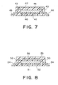
- the MRAM illustrated in Fig. 7 comprises a substrate 41 and an integrated device portion 42 mounted on the substrate 41.
- the integrated device portion 42 is connected through lead wires 43 to lead terminals 44.
- the substrate 41, the integrated device portion 42, the lead wires 43, and the lead terminals 44 are molded by a resin mold 45.
- a high-frequency current suppressor 46 is arranged on a lower surface of the substrate 41.
- the integrated device portion 42 is similar in structure to the integrated device portion 22 illustrated in Fig. 4.
- the high-frequency current suppressor 46 comprises a thin film of a granular magnetic material.
- the thin film can be formed in a manner substantially similar to that of the high-frequency current suppressor 26 in the MRAM described in conjunction with Figs. 3 and 4.
- the thin film is made of a material and has a composition such that no heat treatment is required after deposition by vapor deposition or the like.
- the MRAM illustrated in Fig. 8 comprises a substrate 51 and an integrated device portion 52 mounted on the substrate 51.
- the integrated device portion 52 is connected through lead wires 53 to lead terminals 54.
- the substrate 51, the integrated device portion 52, the lead wires 53, and the lead terminals 54 are molded by a resin mold 55.
- a high-frequency current suppressor 56 is arranged above the integrated device portion 52 with a space kept therefrom.
- the integrated device portion 52 is similar in structure to the integrated device portion 22 illustrated in Fig. 4.
- the high-frequency current suppressor 56 comprises a thin film of a granular magnetic material.
- the thin film can be formed on a polyimide plate in a manner substantially similar to that of the high-frequency current suppressor 27 in the MRAM described in conjunction with Figs. 3 and 4.
- the high-frequency current suppressor 56 thus obtained is arranged above the integrated device portion 52 by molding with the resin mold 55 such as polyimide.
- harmonic distortion of a signal pulse current is decreased and undesired emission or radiation can be reduced. Therefore, it is possible to avoid substantial decrease in data writing speed and in data reading speed.
Landscapes
- Engineering & Computer Science (AREA)
- Chemical & Material Sciences (AREA)
- Computer Hardware Design (AREA)
- Crystallography & Structural Chemistry (AREA)
- Nanotechnology (AREA)
- Power Engineering (AREA)
- Hall/Mr Elements (AREA)
- Thin Magnetic Films (AREA)
- Mram Or Spin Memory Techniques (AREA)
- Semiconductor Memories (AREA)
Abstract
Description
Claims (6)
- A magnetic random access memory comprising:a memory device portion using magnetic material; anda high-frequency current suppressor arranged in the vicinity of said magnetic material for suppressing a high-frequency current which flows in said memory device portion.
- The magnetic random access memory according to claim 1, further comprising a mold body in which said memory device portion and said high-frequency current suppressor are molded.
- The magnetic random access memory according to claim 1 or 2, wherein said high-frequency current suppressor comprises a thin film of a granular magnetic material.
- The magnetic random access memory according to claim 3, wherein said granular magnetic material has a composition represented by M-X-Y where M is a magnetic metal element, Y is one element selected from oxygen, nitrogen, and fluorine, and X is an element other than M and Y.
- The magnetic random access memory according to claim 3 or 4, wherein said granular magnetic material has saturation magnetization corresponding to 35% or more of saturation magnetization of a bulk material comprising M alone.
- The magnetic random access memory according to claim 3 or 4, wherein said granular magnetic material has an electric resistance of about 100µΩ·cm or more.
Applications Claiming Priority (2)
| Application Number | Priority Date | Filing Date | Title |
|---|---|---|---|
| JP2000249452A JP2002064189A (en) | 2000-08-21 | 2000-08-21 | Magnetic random access memory |
| JP2000249452 | 2000-08-21 |
Publications (3)
| Publication Number | Publication Date |
|---|---|
| EP1182665A2 true EP1182665A2 (en) | 2002-02-27 |
| EP1182665A3 EP1182665A3 (en) | 2002-03-06 |
| EP1182665B1 EP1182665B1 (en) | 2003-10-29 |
Family
ID=18739188
Family Applications (1)
| Application Number | Title | Priority Date | Filing Date |
|---|---|---|---|
| EP01119925A Expired - Lifetime EP1182665B1 (en) | 2000-08-21 | 2001-08-17 | MRAM with an effective noise countermeasure |
Country Status (9)
| Country | Link |
|---|---|
| US (1) | US6657246B2 (en) |
| EP (1) | EP1182665B1 (en) |
| JP (1) | JP2002064189A (en) |
| KR (1) | KR20020015293A (en) |
| CN (1) | CN1339800A (en) |
| DE (1) | DE60101074T2 (en) |
| NO (1) | NO20014004L (en) |
| SG (1) | SG100748A1 (en) |
| TW (1) | TW495969B (en) |
Families Citing this family (7)
| Publication number | Priority date | Publication date | Assignee | Title |
|---|---|---|---|---|
| US6903396B2 (en) * | 2002-04-12 | 2005-06-07 | Micron Technology, Inc. | Control of MTJ tunnel area |
| US6936763B2 (en) * | 2002-06-28 | 2005-08-30 | Freescale Semiconductor, Inc. | Magnetic shielding for electronic circuits which include magnetic materials |
| US6950577B2 (en) * | 2002-07-01 | 2005-09-27 | Intel Corporation | Waveguide-based Bragg gratings with spectral sidelobe suppression and method thereof |
| JP4424298B2 (en) * | 2005-10-26 | 2010-03-03 | Tdk株式会社 | Electronic components |
| US20090102015A1 (en) * | 2007-10-17 | 2009-04-23 | Ulrich Klostermann | Integrated Circuit, Memory Cell Array, Memory Cell, Memory Module, Method of Operating an Integrated Circuit, and Method of Manufacturing an Integrated Circuit |
| DE102007049786A1 (en) * | 2007-10-17 | 2009-04-23 | Qimonda Ag | Integrated circuit has multiple resistance change memory cells, where each memory cell has top electrode, bottom electrode and resistance changing material provided between top electrode and bottom electrode |
| KR102354370B1 (en) | 2015-04-29 | 2022-01-21 | 삼성전자주식회사 | Magneto-resistive chip package including a shielding structure |
Family Cites Families (10)
| Publication number | Priority date | Publication date | Assignee | Title |
|---|---|---|---|---|
| FI117224B (en) | 1994-01-20 | 2006-07-31 | Nec Tokin Corp | Electromagnetic piece for removing interference, as well as electronic device and hybrid microcircuit element in which it is used |
| AU2371795A (en) * | 1994-05-17 | 1995-12-05 | Olin Corporation | Electronic packages with improved electrical performance |
| JPH0935927A (en) | 1995-07-20 | 1997-02-07 | Tokin Corp | Composite magnetic material and electromagnetic interference suppressor using the same |
| US5741435A (en) * | 1995-08-08 | 1998-04-21 | Nano Systems, Inc. | Magnetic memory having shape anisotropic magnetic elements |
| US6001272A (en) * | 1996-03-18 | 1999-12-14 | Seiko Epson Corporation | Method for producing rare earth bond magnet, composition for rare earth bond magnet, and rare earth bond magnet |
| JPH10163400A (en) * | 1996-11-28 | 1998-06-19 | Nitto Denko Corp | Semiconductor device and two-layer lead frame used therefor |
| US5902690A (en) | 1997-02-25 | 1999-05-11 | Motorola, Inc. | Stray magnetic shielding for a non-volatile MRAM |
| JPH10307902A (en) | 1997-05-01 | 1998-11-17 | Tokin Corp | Protection device and protection method for IC card |
| SG100666A1 (en) * | 2000-04-04 | 2003-12-26 | Nec Tokin Corp | Wiring board comprising granular magnetic film |
| JP2001291989A (en) * | 2000-04-04 | 2001-10-19 | Tokin Corp | Electronic components with metal housing |
-
2000
- 2000-08-21 JP JP2000249452A patent/JP2002064189A/en active Pending
-
2001
- 2001-08-10 US US09/927,974 patent/US6657246B2/en not_active Expired - Fee Related
- 2001-08-16 TW TW090120078A patent/TW495969B/en not_active IP Right Cessation
- 2001-08-16 NO NO20014004A patent/NO20014004L/en unknown
- 2001-08-17 DE DE60101074T patent/DE60101074T2/en not_active Expired - Fee Related
- 2001-08-17 EP EP01119925A patent/EP1182665B1/en not_active Expired - Lifetime
- 2001-08-18 SG SG200105075A patent/SG100748A1/en unknown
- 2001-08-21 CN CN01125743A patent/CN1339800A/en active Pending
- 2001-08-21 KR KR1020010050200A patent/KR20020015293A/en not_active Withdrawn
Also Published As
| Publication number | Publication date |
|---|---|
| SG100748A1 (en) | 2003-12-26 |
| US6657246B2 (en) | 2003-12-02 |
| NO20014004L (en) | 2003-02-24 |
| TW495969B (en) | 2002-07-21 |
| CN1339800A (en) | 2002-03-13 |
| DE60101074T2 (en) | 2004-07-15 |
| JP2002064189A (en) | 2002-02-28 |
| KR20020015293A (en) | 2002-02-27 |
| NO20014004D0 (en) | 2001-08-16 |
| US20020020865A1 (en) | 2002-02-21 |
| EP1182665B1 (en) | 2003-10-29 |
| DE60101074D1 (en) | 2003-12-04 |
| EP1182665A3 (en) | 2002-03-06 |
Similar Documents
| Publication | Publication Date | Title |
|---|---|---|
| US6534708B2 (en) | Signal transmission cable with a noise absorbing high loss magnetic film formed on a sheath of the cable | |
| EP1518451B1 (en) | Magnetic shielding for electronic circuits which include magnetic materials | |
| Otani et al. | Magnetic and transport properties of sub-micron ferromagnetic wires | |
| JP4398056B2 (en) | Resin mold body | |
| EP1182665B1 (en) | MRAM with an effective noise countermeasure | |
| US6953899B1 (en) | Wiring board comprising granular magnetic film | |
| KR20010095254A (en) | Electronic component comprising a metallic case provided with a magnetic loss material | |
| US6635961B2 (en) | Electronic component of a high frequency current suppression type and bonding wire for the same | |
| JP4417521B2 (en) | Wiring board | |
| JP4287020B2 (en) | High frequency current suppression type heat sink | |
| KR100845370B1 (en) | Electromagnetic noise suppressing thin film | |
| EP1166288B1 (en) | Magnetic substance with maximum complex permeability in quasi-microwave band and method for production of the same | |
| JP4271825B2 (en) | Semiconductor bare chip and semiconductor wafer | |
| JP4398057B2 (en) | High frequency current suppression type electronic components | |
| JP4243000B2 (en) | High frequency current suppressing bonding wire for electronic components and electronic component including the same | |
| JP2001284755A (en) | Wiring board | |
| JP2001284132A (en) | Magnetic core | |
| JP2001284698A (en) | Light emitting element | |
| JP2001284947A (en) | Antenna using high frequency current suppressor |
Legal Events
| Date | Code | Title | Description |
|---|---|---|---|
| PUAI | Public reference made under article 153(3) epc to a published international application that has entered the european phase |
Free format text: ORIGINAL CODE: 0009012 |
|
| PUAL | Search report despatched |
Free format text: ORIGINAL CODE: 0009013 |
|
| AK | Designated contracting states |
Kind code of ref document: A2 Designated state(s): DE FI FR GB SE Kind code of ref document: A2 Designated state(s): AT BE CH CY DE DK ES FI FR GB GR IE IT LI LU MC NL PT SE TR |
|
| AX | Request for extension of the european patent |
Free format text: AL;LT;LV;MK;RO;SI |
|
| AK | Designated contracting states |
Kind code of ref document: A3 Designated state(s): AT BE CH CY DE DK ES FI FR GB GR IE IT LI LU MC NL PT SE TR |
|
| AX | Request for extension of the european patent |
Free format text: AL;LT;LV;MK;RO;SI |
|
| RAP1 | Party data changed (applicant data changed or rights of an application transferred) |
Owner name: NEC TOKIN CORPORATION |
|
| 17P | Request for examination filed |
Effective date: 20020830 |
|
| AKX | Designation fees paid |
Free format text: DE FI FR GB SE |
|
| 17Q | First examination report despatched |
Effective date: 20021023 |
|
| GRAH | Despatch of communication of intention to grant a patent |
Free format text: ORIGINAL CODE: EPIDOS IGRA |
|
| GRAS | Grant fee paid |
Free format text: ORIGINAL CODE: EPIDOSNIGR3 |
|
| GRAA | (expected) grant |
Free format text: ORIGINAL CODE: 0009210 |
|
| RIN1 | Information on inventor provided before grant (corrected) |
Inventor name: MASUMOTO, TOSHIAKI, C/O NEC TOKIN CORPORATION Inventor name: YOSHIDA, SHIGEYOSHI, C/O NEC TOKIN CORPORATION Inventor name: ONO, HIROSHI,C/O NEC TOKIN CORPORATION |
|
| AK | Designated contracting states |
Kind code of ref document: B1 Designated state(s): DE FI FR GB SE |
|
| REG | Reference to a national code |
Ref country code: GB Ref legal event code: FG4D |
|
| RTI1 | Title (correction) |
Free format text: MRAM WITH AN EFFECTIVE NOISE COUNTERMEASURE |
|
| REG | Reference to a national code |
Ref country code: IE Ref legal event code: FG4D |
|
| REF | Corresponds to: |
Ref document number: 60101074 Country of ref document: DE Date of ref document: 20031204 Kind code of ref document: P |
|
| REG | Reference to a national code |
Ref country code: SE Ref legal event code: TRGR |
|
| ET | Fr: translation filed | ||
| PGFP | Annual fee paid to national office [announced via postgrant information from national office to epo] |
Ref country code: FI Payment date: 20040819 Year of fee payment: 4 |
|
| PLBE | No opposition filed within time limit |
Free format text: ORIGINAL CODE: 0009261 |
|
| STAA | Information on the status of an ep patent application or granted ep patent |
Free format text: STATUS: NO OPPOSITION FILED WITHIN TIME LIMIT |
|
| 26N | No opposition filed |
Effective date: 20040730 |
|
| REG | Reference to a national code |
Ref country code: IE Ref legal event code: MM4A |
|
| PGFP | Annual fee paid to national office [announced via postgrant information from national office to epo] |
Ref country code: SE Payment date: 20050804 Year of fee payment: 5 |
|
| PGFP | Annual fee paid to national office [announced via postgrant information from national office to epo] |
Ref country code: FR Payment date: 20050809 Year of fee payment: 5 |
|
| PG25 | Lapsed in a contracting state [announced via postgrant information from national office to epo] |
Ref country code: FI Free format text: LAPSE BECAUSE OF NON-PAYMENT OF DUE FEES Effective date: 20050817 |
|
| PGFP | Annual fee paid to national office [announced via postgrant information from national office to epo] |
Ref country code: DE Payment date: 20060810 Year of fee payment: 6 |
|
| PGFP | Annual fee paid to national office [announced via postgrant information from national office to epo] |
Ref country code: GB Payment date: 20060816 Year of fee payment: 6 |
|
| PG25 | Lapsed in a contracting state [announced via postgrant information from national office to epo] |
Ref country code: SE Free format text: LAPSE BECAUSE OF NON-PAYMENT OF DUE FEES Effective date: 20060818 |
|
| EUG | Se: european patent has lapsed | ||
| REG | Reference to a national code |
Ref country code: FR Ref legal event code: ST Effective date: 20070430 |
|
| GBPC | Gb: european patent ceased through non-payment of renewal fee |
Effective date: 20070817 |
|
| PG25 | Lapsed in a contracting state [announced via postgrant information from national office to epo] |
Ref country code: FR Free format text: LAPSE BECAUSE OF NON-PAYMENT OF DUE FEES Effective date: 20060831 |
|
| PG25 | Lapsed in a contracting state [announced via postgrant information from national office to epo] |
Ref country code: DE Free format text: LAPSE BECAUSE OF NON-PAYMENT OF DUE FEES Effective date: 20080301 |
|
| PG25 | Lapsed in a contracting state [announced via postgrant information from national office to epo] |
Ref country code: GB Free format text: LAPSE BECAUSE OF NON-PAYMENT OF DUE FEES Effective date: 20070817 |