EP1182484A2 - Optical fiber separation and regrouping device - Google Patents
Optical fiber separation and regrouping device Download PDFInfo
- Publication number
- EP1182484A2 EP1182484A2 EP01117722A EP01117722A EP1182484A2 EP 1182484 A2 EP1182484 A2 EP 1182484A2 EP 01117722 A EP01117722 A EP 01117722A EP 01117722 A EP01117722 A EP 01117722A EP 1182484 A2 EP1182484 A2 EP 1182484A2
- Authority
- EP
- European Patent Office
- Prior art keywords
- housing
- optical fibers
- conductive elements
- input
- fibers
- Prior art date
- Legal status (The legal status is an assumption and is not a legal conclusion. Google has not performed a legal analysis and makes no representation as to the accuracy of the status listed.)
- Granted
Links
Images




Classifications
-
- C—CHEMISTRY; METALLURGY
- C03—GLASS; MINERAL OR SLAG WOOL
- C03B—MANUFACTURE, SHAPING, OR SUPPLEMENTARY PROCESSES
- C03B37/00—Manufacture or treatment of flakes, fibres, or filaments from softened glass, minerals, or slags
- C03B37/01—Manufacture of glass fibres or filaments
- C03B37/02—Manufacture of glass fibres or filaments by drawing or extruding, e.g. direct drawing of molten glass from nozzles; Cooling fins therefor
- C03B37/03—Drawing means, e.g. drawing drums ; Traction or tensioning devices
- C03B37/035—Drawing means, e.g. drawing drums ; Traction or tensioning devices having means for deflecting or stripping-off fibres or for removing defective parts
-
- G—PHYSICS
- G02—OPTICS
- G02B—OPTICAL ELEMENTS, SYSTEMS OR APPARATUS
- G02B6/00—Light guides; Structural details of arrangements comprising light guides and other optical elements, e.g. couplings
- G02B6/44—Mechanical structures for providing tensile strength and external protection for fibres, e.g. optical transmission cables
- G02B6/4439—Auxiliary devices
- G02B6/4471—Terminating devices ; Cable clamps
- G02B6/44715—Fan-out devices
-
- G—PHYSICS
- G02—OPTICS
- G02B—OPTICAL ELEMENTS, SYSTEMS OR APPARATUS
- G02B6/00—Light guides; Structural details of arrangements comprising light guides and other optical elements, e.g. couplings
- G02B6/44—Mechanical structures for providing tensile strength and external protection for fibres, e.g. optical transmission cables
- G02B6/4439—Auxiliary devices
- G02B6/4471—Terminating devices ; Cable clamps
- G02B6/44765—Terminating devices ; Cable clamps with means for strain-relieving to exterior cable layers
Definitions
- This invention relates generally to a shuffle device, and more particularly, to an optical fiber separation and regrouping device for an optical shuffle.
- the invention further relates to a method of organizing and managing optical fibers.
- Optical fibers provide a well-known medium for conveying information in data and communications systems, such as computer and telephone systems. It is well known, that optical fibers possess characteristics wherein their light transmission capability is greatest when the fiber is straight and devoid of bends, and that they are subject to signal attenuation due to bending. These bending losses can be characterized as losses due to larger, gradual bends (macrobends), and losses due to much smaller and sharper bends (microbends). Macrobends can result from winding the fiber, for example, while microbends arise because of random variations in direction of the core axis.
- Optical fibers are typically provided with protective coatings to preserve the inherent strength of the glass and to buffer the fiber from microbending induced attenuation.
- Individual optical fibers can be encapsulated in a polymer casing that protects the fiber from damage, or an optical fiber ribbon can be formed by aligning a plurality of optical fibers in a linear array and then encapsulating the fiber array in a polymer casing to form the ribbon.
- the first coating which is typically applied to the surface of the optical fiber, is generally referred to as the primary coating.
- the primary coating once cured, is a soft, rubbery material that serves as a buffer to protect the fiber by relieving the stress created when the fiber is bent.
- the primary coating usually has a low glass transition temperature to provide resistance to microbending.
- the primary coating must maintain adequate adhesion to the glass fiber during thermal and hydrolytic aging, yet be strippable for splicing purposes.
- the modulus of the primary coating must be low to cushion and to protect the fiber by relieving stress on the fiber, which can induce microbending and, consequently, inefficient signal transmission. It is desirable for the primary coating to have a low glass transition temperature to ensure that the coating remains in a rubbery state throughout a broad temperature range.
- the secondary or outer coating is applied over the primary coating.
- the secondary coating functions as a hard, protective layer that prevents damage to the glass fiber during processing and use by providing desired resistance to handling forces, such as those encountered when the coated fiber is cabled.
- optical shuffle in which one fiber output from each system is directed to a different system is known as a perfect shuffle.
- an optical shuffle can be formed in one way by which an optical shuffle can be formed. That is, the stripped fibers can be grouped differently, re-encapsulated, and then output from the shuffle. Thus, a discontinuity is created in the area of re-ribbonization, and the fibers can remain undesirably exposed in that region. Moreover, the fibers are prone to strain and bending in the area of the discontinuity.
- the present invention relates to a separation and regrouping device comprising a housing and a plurality of conductive elements, such as optical fibers, extending through an interior region of the housing.
- the optical fibers can be encapsulated individually as fiber optic cables, or grouped together and then encapsulated to form optical fiber ribbons.
- Each optical fiber has a first coating disposed along a first portion thereof, and a second coating disposed along a second portion thereof.
- An encapsulation discontinuity is formed on each optical fiber between the first coating and the second coating.
- the housing can be pre-assembled or molded over the optical fibers to contain the optical fibers and surround the encapsulation discontinuities.
- the interior region of the housing can include a guide channel that channels the optical fibers through the interior region of the housing.
- the guide channel can be a single channel, or can include a plurality of channels.
- the guide channel can also be twisted to rotate the fibers as they extend through the housing.
- the device can also include one or more strain relief elements within the interior region of the housing that contain the optical fibers and surround the encapsulation discontinuities.
- a single strain relief element can contain a plurality of fibers, or the device can include a plurality of strain relief elements, each of which contains a single fiber.
- the housing can also include one or more potting chambers in which the optical fibers can be potted to the housing.
- a method for organizing conductive elements includes providing a plurality of conductive elements arranged in first groups, separating the first groups into individual conductive elements, and rearranging the individual conductive elements into second groups.
- the first groups can be optical fiber ribbons, which are separated by unribbonizing the fibers ( e . g ., by stripping the encapsulation from the ribbon to expose the fibers).
- the unribbonized fibers can then be re-ribbonized ( i . e ., rearranged into a second group and encapsulated to form a second ribbon).
- a method for managing a plurality of conductive elements includes arranging a first section of the conductive elements in a first arrangement, arranging a second section of the conductive elements in a second arrangement, and enclosing a third section of the conductive elements located between the first and second sections.
- the third section of the elements can be enclosed by inserting the conductive elements in a pre-assembled shuffle device, or by encapsulating the conductive elements such as by overmolding a housing over the third section, or by potting the third section within a tubular structure.
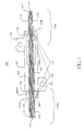
- a separation and regrouping device 100 for conductive elements such as optical fibers comprises a housing 102, and a plurality of optical fibers 110.
- Housing 102 has an input end 102A, an interior region 104, and an output end 102B through which optical fibers 110 extend.
- Each optical fiber 110 is coated with a respective first coating 110' disposed along a first, or input, portion 110A thereof.
- An individual optical fiber 110 can be coated along its input portion 110A to form an input cable 112, or a set of optical fibers 110 can be arrayed and coated together along their respective input portions to form an input ribbon 114.
- Device 100 can include any number of input cables 112 or input ribbons 114, or any combination of input cables 112 and input ribbons 114.
- the set of input cables 112 and input ribbons 114 can be configured as an input fiber matrix 116 as shown in cross section in Figure 2.
- input matrix 116 can include three input ribbons 114a-c, each having six optical fibers 110a-c, respectively, although input matrix 116 can comprise any number or combination of input ribbons 114 or input cables 112, and, in general, an input ribbon 114 can include any number of fibers from 1 to N.
- an input cable 112 can be said to be an input ribbon 114 having only one optical fiber 110.
- input matrix 116 is oriented so that the ribbons 114 are parallel to the direction indicated by arrow C.
- housing 102 is shown to include an input aperture 120 that receives the entire input fiber matrix 116.
- housing 102 can include a guide channel 142 that guides fibers 110 through interior region 104 of housing 102.
- guide channel 142 includes a plurality of channels 144 that extend through housing 102.
- Each channel 144 is sized and shaped to accommodate either a discrete cable 112 or a ribbon 114 of fibers.
- Each optical fiber 110 is coated with a respective second coating 110" disposed along a second, or output, portion 110B thereof.
- An individual optical fiber 110 can be coated along its output portion 110B to form an output cable 122, or a set of optical fibers 110 can be arrayed and coated together along their respective output portions to form an output ribbon 124.
- Device 100 can include any number of output cables 122 or output ribbons 124, or any combination of output cables 122 and output ribbons 124, although the total number of optical fibers 110 that extend through output end 102B of housing 102 should equal the number of optical fibers 110 that extend through input end 102A of housing 102.
- any or all of the input ribbons can extend through housing 102 and emerge from output end 102B in the same configuration (i.e ., the same fibers are grouped together on output as on input), device 100 can be used to separate the array of fibers that form an input ribbon 114, and then regroup and re-ribbonize a second array of fibers, on the output side of the device, to form an output ribbon 124.
- Figures 3A and 3B provide cross sectional views of an unrotated output fiber matrix 118 before and after re-ribbonization.
- output matrix 118 is oriented so that output ribbons 124 are parallel to the direction indicated by arrow C
- re-ribbonized output matrix 118' is oriented so that output ribbons 124' are perpendicular to the direction indicated by arrow C.
- Output matrix 118 can be re-ribbonized in any manner known to those in the art, although it is preferred that the encapsulation is removed from a distal portion of each ribbon by peeling, or through the use of chemicals or heat strippers, or by any other suitable technique known in the art, to expose optical fibers 110.
- the exposed fibers are preferably encapsulated to form a plurality of output ribbons 124a'-f'.
- each output ribbon 124a'-f' includes one fiber 110 from each input ribbon 114a-c.
- a respective encapsulation discontinuity 130 is formed on each optical fiber 110 where optical fiber 110 has no coating ( i . e ., the between its first, or input, coating 110', and its second, or output, coating 110").
- all the respective encapsulation discontinuities 130 are formed in the same general area, or region 132, within housing 102.
- fiber separation and regrouping device 100 can also include one or more optional strain relief elements.
- Device 100 can include a single strain relief element 134 that surrounds all the fibers 110 in region 132 at the output end of housing 102.
- strain relief element 134 is a small, plastic tube that contains a plurality of fibers (preferably, all of them) to keep them from bending in region 132.
- device 100 can include one or more individual strain relief elements 136 that surround the respective discontinuities 130 of individual optical fibers 110 or where the ribbons 114 have been separated into discrete cables 112 at the input end of housing 102.
- each strain relief element 136 is a small, plastic tube that contains an individual optical fiber 110 to keep it from bending at its encapsulation discontinuity 130.
- housing 102 can include an input potting chamber 140A for potting input cables 112 and input ribbons 114.
- housing 102 can include an output potting chamber 140B for potting output cables and ribbons.
- the potting chambers 140A, 140B can be filled with epoxy or other such potting material to hold the fibers in place. This stabilizes the fibers (and strain relief elements 134, 136, if present) and thereby reduces strain.
- device 100 can serve to enclose the fibers, without the need for any additional housing.
- output ribbons 124' are oriented in the same direction as input ribbons 112a-c (see Figure 2).
- output ribbons 124' can be oriented in any direction relative to input ribbons 112, it is preferred, for routing purposes, that output ribbons 124' are in the same orientation as input ribbons 112, that is, generally parallel to the direction of arrow C.
- a device according to the present invention can be used to rotate the ribbon matrix as it extends though the housing so that, after re-ribbonization, the output ribbons are oriented in the same direction as the input ribbons.
- Device 100 can also include one or more mounting members 146 that extend from housing 102.
- Mounting members 146 can be used to mount device 100 to one or more substrates, such as printed circuit boards (PCBs).
- PCBs printed circuit boards
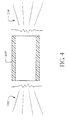
- housing 102 could be molded over the optical fibers at region 132 to contain the fibers and reduce the incidence of bending in region 132.
- housing 102 can be made of a polymer, such as plastic, and is molded over the optical fibers.
- housing 102' could be a generally tubular structure with open ends and an open interior. Once the fibers 110 are passed therethrough, housing 102' could then be potted with known materials, such as epoxy. The epoxy fills the remainder of the open interior of the housing not occupied by the fibers. The epoxy retains the fibers in position and provides strain relief.
- Figure 5 shows a cross-section of a device 200 for separating and regrouping optical fibers that includes twisted guide channels 144.
- Device 200 is similar to device 100, except that channels 144 are twisted.
- the fiber matrix is rotated from a first orientation at input end 102A (as shown in Figure 2) into a second orientation at output end 102B (as shown in Figure 6A) because of the twists.
- Output fiber matrix 118 can now be "re-ribbonized,” as described above, to form a rotated re-ribbonized output fiber matrix 118", a cross sectional view of which is depicted in Figure 6B. Note that output ribbons 124"a-f are once again parallel to the direction given by arrow C.
- the output fiber matrix can, in general, have any orientation relative to the orientation of the input fiber matrix, (i.e ., guide channel 144 can be twisted to rotate the fiber matrix any number of degrees), it is preferred that guide channel 144 is twisted to rotate the fiber matrix approximately 90 degrees so that the output ribbons after re-ribbonization can be made parallel to the input ribbons. This helps to reduce the overall size of the device.
- a fiber device according to the present invention can be sized for any application, although it is usually desirable that the device be as small as possible, especially for applications where available space is limited.
- device 100 can be about 50 mm long and have a cross section of about 10 mm x 10 mm.
Landscapes
- Physics & Mathematics (AREA)
- Chemical & Material Sciences (AREA)
- Optics & Photonics (AREA)
- General Physics & Mathematics (AREA)
- Engineering & Computer Science (AREA)
- Organic Chemistry (AREA)
- Geochemistry & Mineralogy (AREA)
- General Life Sciences & Earth Sciences (AREA)
- Manufacturing & Machinery (AREA)
- Materials Engineering (AREA)
- Life Sciences & Earth Sciences (AREA)
- Light Guides In General And Applications Therefor (AREA)
- Mechanical Coupling Of Light Guides (AREA)
- Laser Surgery Devices (AREA)
- Paper (AREA)
- Filtering Materials (AREA)
- External Artificial Organs (AREA)
Abstract
Description
Claims (20)
- A fiber separation and regrouping device (100, 200), comprising:wherein the housing (102) is molded over the optical fibers (110) to contain the optical fibers (110) and surround the respective encapsulation discontinuities (130).a housing (102) having an input end (102A), an output end (102B), and an interior region (104) extending between the input end (102A) and the output end (102B) thereof; anda plurality of optical fibers (110) extending through the interior region (104) of the housing (102), each said optical fiber (110) having a respective first coating (110') disposed along a first portion (110A) thereof and a respective second coating (110") disposed along a second portion (110B) thereof, wherein a respective encapsulation discontinuity (130) is formed on each said optical fiber (110) between the respective first coating (110') and the respective second coating (110"),
- The device (100, 200) of claim 1, further comprising:at least one strain relief element (134, 136) within the interior region (104) of the housing (102) that contains at least one of the optical fibers (110) and surrounds the respective encapsulation discontinuity (130) of the at least one optical fiber (110).
- The device (100, 200) of claim 1 or 2, wherein the strain relief element (134, 136) contains the plurality of fibers (110) and surrounds the respective encapsulation discontinuities (130).
- The device (100, 200) of claim 1, 2 or 3, further comprising a plurality of strain relief elements (134, 136) within the interior region (104) of the housing (102), each said strain relief element (134, 136) containing one of the optical fibers (110) and surrounding the respective encapsulation discontinuity (130) thereof.
- The device (100, 200) of claim 1, 2, 3 or 4, wherein the housing (102) comprises an input potting chamber (140A) proximate the input end (102A) thereof in which the optical fibers (110) are potted to the housing (102).
- The device (100, 200) of one of the foregoing claims, wherein the housing (102) comprises an output potting chamber (140B) proximate the output end (102B) thereof in which the optical fibers (110) are potted to the housing (102).
- The device (100, 200) of one of the foregoing claims, wherein the input end (102A) of the housing (102) includes a plurality of input apertures (120) through which optical fibers (110) extend into the interior region (104) thereof.
- The device (100, 200) of one of the foregoing claims, wherein at least a subset of the plurality of optical fibers (110) form an input fiber optic ribbon (114) extending through the input end (102A) of the housing (102).
- The device (100, 200) of one of the foregoing claims, wherein at least a subset of the plurality of optical fibers (110) form an output fiber optic ribbon (124) extending through the output end (102B) of the housing (102).
- The device (100, 200) of one of the foregoing claims, wherein the interior region (104) of the housing (102) includes a guide channel (142), in particular a plurality of guide channels, that channels the optical fibers (110) through the interior region (104) of the housing (102).
- The device of claim 1, wherein the interior region of the housing includes a twisted guide channel (144), in particular a plurality of guide channels, that rotates the optical fibers (110) as they extend through the housing (102).
- A method of organizing conductive elements, in particular optical fibers (110), comprising the steps ofproviding a plurality of conductive elements arranged in first groups (114a-c);separating said first groups into individual conductive elements; rearranging said individual conductive elements into second groups; andextending said conductive elements through a shuffle device (110, 200).
- The method as recited in claim 12, wherein said first groups comprise ribbons (114a-b), and said separating step comprises unribbonizing said first groups.
- The method as recited in claim 12 or 13, further comprising the step of placing said second group in ribbons (124a-c, 124a'-f', 124a"-f").
- The method as recited in claim 12, 13 or 14, wherein the rearranging step produces second groups different from said first groups.
- A method of managing a plurality of conductive elements, in particular optical fibers (110), comprising the steps of:arranging a first section (114) of said conductive elements in a first arrangement (116);arranging a second section (124) of said conductive elements in a second arrangement (118, 118', 118"); andenclosing a third section of said conductive elements located between said first section (116) and said second section (118, 118', 118").
- The method as recited in claim 16, wherein the enclosing step comprises inserting said conductive elements in a pre-assembled shuffle device (100, 200).
- The method as recited in claim 16, wherein the enclosing step comprises encapsulating said conductive elements.
- The method as recited in claim 18, wherein the encapsulating step comprises overmolding a housing (102) over said third section.
- The method as recited in claim 18, wherein the encapsulating step comprises the steps of:placing said third section in a tubular structure (102'); andpotting said third section within said tubular structure (102').
Applications Claiming Priority (2)
| Application Number | Priority Date | Filing Date | Title |
|---|---|---|---|
| US09/638,768 US6594437B1 (en) | 2000-08-15 | 2000-08-15 | Optical fiber separation and regrouping device |
| US638768 | 2000-08-15 |
Publications (3)
| Publication Number | Publication Date |
|---|---|
| EP1182484A2 true EP1182484A2 (en) | 2002-02-27 |
| EP1182484A3 EP1182484A3 (en) | 2004-06-09 |
| EP1182484B1 EP1182484B1 (en) | 2006-12-06 |
Family
ID=24561335
Family Applications (1)
| Application Number | Title | Priority Date | Filing Date |
|---|---|---|---|
| EP01117722A Expired - Lifetime EP1182484B1 (en) | 2000-08-15 | 2001-07-27 | Optical fiber separation and regrouping device |
Country Status (8)
| Country | Link |
|---|---|
| US (2) | US6594437B1 (en) |
| EP (1) | EP1182484B1 (en) |
| JP (1) | JP2002098841A (en) |
| KR (1) | KR20020013804A (en) |
| AT (1) | ATE347703T1 (en) |
| CA (1) | CA2353508A1 (en) |
| DE (1) | DE60124994T2 (en) |
| MX (1) | MXPA01007997A (en) |
Cited By (3)
| Publication number | Priority date | Publication date | Assignee | Title |
|---|---|---|---|---|
| WO2007103439A3 (en) * | 2006-03-09 | 2007-12-06 | Adc Telecommunications Inc | Mid-span breakout with helical fiber routing |
| US7532799B2 (en) | 2007-04-12 | 2009-05-12 | Adc Telecommunications | Fiber optic telecommunications cable assembly |
| US7609925B2 (en) | 2007-04-12 | 2009-10-27 | Adc Telecommunications, Inc. | Fiber optic cable breakout configuration with tensile reinforcement |
Families Citing this family (8)
| Publication number | Priority date | Publication date | Assignee | Title |
|---|---|---|---|---|
| US6960030B2 (en) * | 2002-06-05 | 2005-11-01 | The Furukawa Electric Co., Ltd. | Optical connector boot with controlled rotation feature |
| US7088893B2 (en) * | 2003-11-26 | 2006-08-08 | Corning Cable Systems Llc | Pre-connectorized fiber optic distribution cable having multifiber connector |
| US7125494B2 (en) * | 2004-06-02 | 2006-10-24 | Illinois Tool Works, Inc. | Method of removing matrix from fiber optic cable |
| US7303069B2 (en) * | 2005-05-25 | 2007-12-04 | Illinois Tool Works, Inc. | Pre-moistened fiber optic component cleaning tool with integrated platen |
| KR100720527B1 (en) | 2005-12-28 | 2007-05-22 | 동부일렉트로닉스 주식회사 | CMOS image sensor and its manufacturing method |
| DE102008061700B3 (en) * | 2008-12-11 | 2010-02-18 | Jt Optical Engine Gmbh + Co. Kg | Fiber stripping method, involves dipping fiber bundle into chemical solvent upto ingates of fibers for preset time period to pre-weaken of connection between shells and cores of fibers, and removing pre-weakened shell sections from cores |
| US9325604B2 (en) | 2013-03-15 | 2016-04-26 | Plexxi Inc. | System and method for data center optical connection |
| JP2017187678A (en) * | 2016-04-07 | 2017-10-12 | 住友電気工業株式会社 | Optical wiring member |
Family Cites Families (45)
| Publication number | Priority date | Publication date | Assignee | Title |
|---|---|---|---|---|
| US4185888A (en) * | 1962-09-21 | 1980-01-29 | Quelle Fred W Jr | Cryptographic system employing optical scrambling arrays |
| US3883222A (en) | 1973-09-07 | 1975-05-13 | Corning Glass Works | Coupler for optical communication system |
| DE2505995C3 (en) * | 1974-02-16 | 1979-03-01 | Olympus Optical Co., Ltd., Tokio | Method for producing an image decomposer |
| JPS5988710A (en) * | 1982-11-15 | 1984-05-22 | Hitachi Ltd | Plastic multicore optical connector |
| FR2537808A1 (en) | 1982-12-08 | 1984-06-15 | Instruments Sa | OPTICAL COMPONENT WITH SHARED FUNCTION FOR OPTICAL TELETRANSMISSIONS |
| FR2547071B1 (en) | 1983-05-31 | 1986-02-14 | Cit Alcatel | OPTO-ELECTRONIC SPACE SWITCHING DEVICE |
| FR2547150A1 (en) | 1983-05-31 | 1984-12-07 | Cit Alcatel | OPTO-MECHANICAL SWITCH AND SPATIAL SWITCHING ASSEMBLY IMPLEMENTING THE SAME |
| JPS63500131A (en) * | 1985-06-24 | 1988-01-14 | アメリカン テレフオン アンド テレグラフ カムパニ− | optical mixing device |
| KR910004713B1 (en) * | 1987-02-06 | 1991-07-10 | 스미도모덴기 고오교오 가부시기가이샤 | Apparatus for arranging a plurality of coated optical fiber |
| US4824194A (en) * | 1987-03-25 | 1989-04-25 | Fuji Photo Film Co., Ltd. | Light guide apparatus formed from strip light guides |
| US4943136A (en) | 1988-12-09 | 1990-07-24 | The Boeing Company | Optical backplane interconnection |
| JP2718013B2 (en) | 1989-01-12 | 1998-02-25 | 住友電気工業株式会社 | Optical fiber wiring equipment |
| US4952022A (en) * | 1989-03-02 | 1990-08-28 | Xerox Corporation | Fiber optic line illuminator with deformed end fibers and method of making same |
| US5009477A (en) | 1989-05-12 | 1991-04-23 | At&T Bell Laboratories | Optical interconnect arrangement |
| US4932747A (en) * | 1989-09-07 | 1990-06-12 | The United States Of America As Represented By The Secretary Of The Navy | Fiber bundle homogenizer and method utilizing same |
| US4995692A (en) | 1990-02-06 | 1991-02-26 | General Motors Corporation | Fiber optic star coupler |
| JPH04889A (en) * | 1990-04-17 | 1992-01-06 | Asahi Optical Co Ltd | Light incident device for auto-white balance sensor |
| US5335306A (en) * | 1991-04-04 | 1994-08-02 | Shin-Etsu Chemical Co., Ltd. | Ultraviolet resistant silica glass fiber |
| US5155785A (en) | 1991-05-01 | 1992-10-13 | At&T Bell Laboratories | Optical fiber interconnection apparatus and method |
| US5185840A (en) * | 1991-05-06 | 1993-02-09 | Computer Crafts, Inc. | Branching method for a multi-fiber fiberoptic cable |
| US5309538A (en) * | 1991-09-06 | 1994-05-03 | Minnesota Mining And Manufacturing Company | Reinforced multiple optical fiber splice having preanodized element |
| US5239609A (en) | 1992-03-03 | 1993-08-24 | Porta Systems Corp. | Means for routing buffer tube type fiber optical cable |
| US5303373A (en) | 1992-10-16 | 1994-04-12 | Schott Fiber Optics, Inc. | Anamorphic fused fiber optic bundle |
| JPH0792342A (en) * | 1993-07-29 | 1995-04-07 | Sumitomo Electric Ind Ltd | Optical waveguide module |
| US5394503A (en) * | 1993-10-08 | 1995-02-28 | Data Switch Corporation | Optical fiber connection monitoring apparatus, patch panel control system and method of using same |
| JPH07198968A (en) * | 1993-12-28 | 1995-08-01 | Furukawa Electric Co Ltd:The | Terminal structure of multi-core optical fiber parallel core |
| JPH07230021A (en) * | 1994-02-17 | 1995-08-29 | Nippon Telegr & Teleph Corp <Ntt> | Pitch conversion multi-core optical fiber tape and manufacturing method thereof |
| US5500917A (en) * | 1994-04-18 | 1996-03-19 | Gould Electronics Inc. | Optical assembly/housing for securing optical fiber components, devices and fibers to the same or to mounting fixtures |
| DE4422362B4 (en) * | 1994-06-27 | 2006-11-16 | CCS Technology, Inc., Wilmington | Method for producing a splice connection between at least two optical waveguides |
| US5604830A (en) * | 1994-12-22 | 1997-02-18 | Hoechst Celanese Corp. | Multiple fiber connector for injection molded multiple fiberoptic coupler unit and cladding for same |
| US5715345A (en) * | 1995-02-27 | 1998-02-03 | Hughes Danbury Optical Systems, Inc. | Optical beam regeneration by optical fiber remapping |
| US5862285A (en) * | 1995-08-04 | 1999-01-19 | Ceramoptec Industries, Inc. | Multichannel optical fiber bundle with ordered structure in its sensitive probe tip |
| SE504587C2 (en) * | 1995-10-09 | 1997-03-10 | Ericsson Telefon Ab L M | Fanout device and method of manufacture thereof |
| JP3450104B2 (en) * | 1995-11-13 | 2003-09-22 | 古河電気工業株式会社 | Optical coupler |
| FR2743424B1 (en) | 1996-01-09 | 1998-03-27 | Instruments Sa | WAVELENGTH ROUTER N X N, OPTICAL ROUTING PROCESS AND ASSOCIATED COMMUNICATIONS NETWORK |
| CA2214982A1 (en) * | 1996-01-26 | 1997-07-31 | Sumitomo Electric Industries, Ltd. | Optical waveguide module |
| JP2000512102A (en) | 1996-06-14 | 2000-09-12 | アクゾ ノーベル ナムローゼ フェンノートシャップ | Optical switch matrix |
| US5943455A (en) | 1997-04-18 | 1999-08-24 | Lucent Technologies Inc. | Method and apparatus for interfacing optical fibers from optical fiber ribbons and cables with an optical integrated circuit |
| US5857051A (en) * | 1997-04-21 | 1999-01-05 | Lucent Technologies Inc. | High density riser and plenum breakout cables for indoor and outdoor cable applications |
| US5915055A (en) * | 1997-06-30 | 1999-06-22 | Siecor Corporation | Method and apparatus for connectorizing fiber optic cable |
| SE510068C2 (en) * | 1997-08-22 | 1999-04-12 | Ericsson Telefon Ab L M | Component for cross-coupling of optical fibers |
| US6017154A (en) * | 1998-02-05 | 2000-01-25 | Lucent Technologies, Inc. | Optical fiber connector with cable anchoring means |
| CA2323481C (en) * | 1998-03-12 | 2005-01-11 | Tomoegawa Paper Co., Ltd. | Optical connection component and method of producing the same |
| US6222976B1 (en) * | 1999-06-30 | 2001-04-24 | Lucent Technologies Inc. | Optical harness and cross-connect method |
| US6243520B1 (en) * | 1999-08-16 | 2001-06-05 | Schott Fiber Optics, Inc. | Optical fiber bundle having an aligned optical fiber array and method of fabricating the same |
-
2000
- 2000-08-15 US US09/638,768 patent/US6594437B1/en not_active Expired - Lifetime
-
2001
- 2001-07-16 CA CA002353508A patent/CA2353508A1/en not_active Abandoned
- 2001-07-27 DE DE60124994T patent/DE60124994T2/en not_active Expired - Lifetime
- 2001-07-27 AT AT01117722T patent/ATE347703T1/en not_active IP Right Cessation
- 2001-07-27 EP EP01117722A patent/EP1182484B1/en not_active Expired - Lifetime
- 2001-08-03 JP JP2001236274A patent/JP2002098841A/en active Pending
- 2001-08-08 MX MXPA01007997A patent/MXPA01007997A/en active IP Right Grant
- 2001-08-14 KR KR1020010048888A patent/KR20020013804A/en not_active Ceased
-
2002
- 2002-12-04 US US10/309,715 patent/US20030118313A1/en not_active Abandoned
Cited By (4)
| Publication number | Priority date | Publication date | Assignee | Title |
|---|---|---|---|---|
| WO2007103439A3 (en) * | 2006-03-09 | 2007-12-06 | Adc Telecommunications Inc | Mid-span breakout with helical fiber routing |
| US7590321B2 (en) | 2006-03-09 | 2009-09-15 | Adc Telecommunications, Inc. | Mid-span breakout with helical fiber routing |
| US7532799B2 (en) | 2007-04-12 | 2009-05-12 | Adc Telecommunications | Fiber optic telecommunications cable assembly |
| US7609925B2 (en) | 2007-04-12 | 2009-10-27 | Adc Telecommunications, Inc. | Fiber optic cable breakout configuration with tensile reinforcement |
Also Published As
| Publication number | Publication date |
|---|---|
| US6594437B1 (en) | 2003-07-15 |
| MXPA01007997A (en) | 2003-09-10 |
| KR20020013804A (en) | 2002-02-21 |
| EP1182484B1 (en) | 2006-12-06 |
| ATE347703T1 (en) | 2006-12-15 |
| EP1182484A3 (en) | 2004-06-09 |
| US20030118313A1 (en) | 2003-06-26 |
| DE60124994D1 (en) | 2007-01-18 |
| DE60124994T2 (en) | 2007-09-20 |
| CA2353508A1 (en) | 2002-02-15 |
| JP2002098841A (en) | 2002-04-05 |
Similar Documents
| Publication | Publication Date | Title |
|---|---|---|
| KR0159087B1 (en) | Bonded Array of Fiber Optic Ribbons | |
| US6519399B2 (en) | Fiber optic cable with profiled group of optical fibers | |
| US6498882B1 (en) | Assembly and method for reorganizing planar lightwave circuit channels | |
| EP1436650B1 (en) | Use of an apparatus of cross-connecting optical fibres | |
| EP1203254B1 (en) | Optical fibre cable with single strength member unit in cable outer jacket | |
| US5966489A (en) | Fiber optic ribbon interconnect cable | |
| US5268983A (en) | Round, dry, all dielectric, fan out compact optical fiber cable | |
| CA2058203C (en) | Indented tube for optical ribbon | |
| EP0953857B1 (en) | Optical Fiber | |
| US6594437B1 (en) | Optical fiber separation and regrouping device | |
| US4964691A (en) | Optical fiber cable having optical fibers with various lengths | |
| EP1220237B1 (en) | Cable assembly having ripcords with excess length and ripcords attached to tape | |
| EP4050391A1 (en) | Cable assembly | |
| EP1180708A2 (en) | A rotation device for reorienting an optical fiber ribbon matrix | |
| US6556753B2 (en) | Method for the manufacture of a fiber package incorporating therein dispersion compensating gratings | |
| JPH01137208A (en) | Tape-shaped optical fiber | |
| EP4685534A1 (en) | Flexible optical fiber splitter assembly | |
| EP4685537A1 (en) | Flexible optical fiber splice tray assembly | |
| JP2000171657A (en) | Optical fiber array | |
| JP2002258122A (en) | Ribbon optical fiber cord with optical fiber array | |
| CN114578488B (en) | Optical fiber circuit board unit, optical transmission device and photoelectric hybrid circuit board | |
| JP2001281509A (en) | Branch of multi-core optical fiber | |
| JPH08171028A (en) | Optical waveguide module | |
| JPH10115736A (en) | Optical fiber single fiber |
Legal Events
| Date | Code | Title | Description |
|---|---|---|---|
| PUAI | Public reference made under article 153(3) epc to a published international application that has entered the european phase |
Free format text: ORIGINAL CODE: 0009012 |
|
| AK | Designated contracting states |
Kind code of ref document: A2 Designated state(s): AT BE CH CY DE DK ES FI FR GB GR IE IT LI LU MC NL PT SE TR |
|
| AX | Request for extension of the european patent |
Free format text: AL;LT;LV;MK;RO;SI |
|
| PUAL | Search report despatched |
Free format text: ORIGINAL CODE: 0009013 |
|
| AK | Designated contracting states |
Kind code of ref document: A3 Designated state(s): AT BE CH CY DE DK ES FI FR GB GR IE IT LI LU MC NL PT SE TR |
|
| AX | Request for extension of the european patent |
Extension state: AL LT LV MK RO SI |
|
| 17P | Request for examination filed |
Effective date: 20041130 |
|
| AKX | Designation fees paid |
Designated state(s): AT BE CH CY DE DK ES FI FR GB GR IE IT LI LU MC NL PT SE TR |
|
| 17Q | First examination report despatched |
Effective date: 20050405 |
|
| GRAP | Despatch of communication of intention to grant a patent |
Free format text: ORIGINAL CODE: EPIDOSNIGR1 |
|
| GRAS | Grant fee paid |
Free format text: ORIGINAL CODE: EPIDOSNIGR3 |
|
| GRAA | (expected) grant |
Free format text: ORIGINAL CODE: 0009210 |
|
| RAP1 | Party data changed (applicant data changed or rights of an application transferred) |
Owner name: FCI |
|
| AK | Designated contracting states |
Kind code of ref document: B1 Designated state(s): AT BE CH CY DE DK ES FI FR GB GR IE IT LI LU MC NL PT SE TR |
|
| PG25 | Lapsed in a contracting state [announced via postgrant information from national office to epo] |
Ref country code: IT Free format text: LAPSE BECAUSE OF FAILURE TO SUBMIT A TRANSLATION OF THE DESCRIPTION OR TO PAY THE FEE WITHIN THE PRESCRIBED TIME-LIMIT;WARNING: LAPSES OF ITALIAN PATENTS WITH EFFECTIVE DATE BEFORE 2007 MAY HAVE OCCURRED AT ANY TIME BEFORE 2007. THE CORRECT EFFECTIVE DATE MAY BE DIFFERENT FROM THE ONE RECORDED. Effective date: 20061206 Ref country code: AT Free format text: LAPSE BECAUSE OF FAILURE TO SUBMIT A TRANSLATION OF THE DESCRIPTION OR TO PAY THE FEE WITHIN THE PRESCRIBED TIME-LIMIT Effective date: 20061206 Ref country code: LI Free format text: LAPSE BECAUSE OF FAILURE TO SUBMIT A TRANSLATION OF THE DESCRIPTION OR TO PAY THE FEE WITHIN THE PRESCRIBED TIME-LIMIT Effective date: 20061206 Ref country code: FI Free format text: LAPSE BECAUSE OF FAILURE TO SUBMIT A TRANSLATION OF THE DESCRIPTION OR TO PAY THE FEE WITHIN THE PRESCRIBED TIME-LIMIT Effective date: 20061206 Ref country code: BE Free format text: LAPSE BECAUSE OF FAILURE TO SUBMIT A TRANSLATION OF THE DESCRIPTION OR TO PAY THE FEE WITHIN THE PRESCRIBED TIME-LIMIT Effective date: 20061206 Ref country code: NL Free format text: LAPSE BECAUSE OF FAILURE TO SUBMIT A TRANSLATION OF THE DESCRIPTION OR TO PAY THE FEE WITHIN THE PRESCRIBED TIME-LIMIT Effective date: 20061206 Ref country code: DK Free format text: LAPSE BECAUSE OF FAILURE TO SUBMIT A TRANSLATION OF THE DESCRIPTION OR TO PAY THE FEE WITHIN THE PRESCRIBED TIME-LIMIT Effective date: 20061206 Ref country code: CH Free format text: LAPSE BECAUSE OF FAILURE TO SUBMIT A TRANSLATION OF THE DESCRIPTION OR TO PAY THE FEE WITHIN THE PRESCRIBED TIME-LIMIT Effective date: 20061206 |
|
| REG | Reference to a national code |
Ref country code: GB Ref legal event code: FG4D |
|
| REG | Reference to a national code |
Ref country code: CH Ref legal event code: EP |
|
| REG | Reference to a national code |
Ref country code: IE Ref legal event code: FG4D |
|
| REF | Corresponds to: |
Ref document number: 60124994 Country of ref document: DE Date of ref document: 20070118 Kind code of ref document: P |
|
| PG25 | Lapsed in a contracting state [announced via postgrant information from national office to epo] |
Ref country code: SE Free format text: LAPSE BECAUSE OF FAILURE TO SUBMIT A TRANSLATION OF THE DESCRIPTION OR TO PAY THE FEE WITHIN THE PRESCRIBED TIME-LIMIT Effective date: 20070306 |
|
| PG25 | Lapsed in a contracting state [announced via postgrant information from national office to epo] |
Ref country code: ES Free format text: LAPSE BECAUSE OF FAILURE TO SUBMIT A TRANSLATION OF THE DESCRIPTION OR TO PAY THE FEE WITHIN THE PRESCRIBED TIME-LIMIT Effective date: 20070317 |
|
| ET | Fr: translation filed | ||
| PG25 | Lapsed in a contracting state [announced via postgrant information from national office to epo] |
Ref country code: PT Free format text: LAPSE BECAUSE OF FAILURE TO SUBMIT A TRANSLATION OF THE DESCRIPTION OR TO PAY THE FEE WITHIN THE PRESCRIBED TIME-LIMIT Effective date: 20070507 |
|
| NLV1 | Nl: lapsed or annulled due to failure to fulfill the requirements of art. 29p and 29m of the patents act | ||
| REG | Reference to a national code |
Ref country code: CH Ref legal event code: PL |
|
| PLBE | No opposition filed within time limit |
Free format text: ORIGINAL CODE: 0009261 |
|
| STAA | Information on the status of an ep patent application or granted ep patent |
Free format text: STATUS: NO OPPOSITION FILED WITHIN TIME LIMIT |
|
| 26N | No opposition filed |
Effective date: 20070907 |
|
| PG25 | Lapsed in a contracting state [announced via postgrant information from national office to epo] |
Ref country code: MC Free format text: LAPSE BECAUSE OF NON-PAYMENT OF DUE FEES Effective date: 20070731 Ref country code: GR Free format text: LAPSE BECAUSE OF FAILURE TO SUBMIT A TRANSLATION OF THE DESCRIPTION OR TO PAY THE FEE WITHIN THE PRESCRIBED TIME-LIMIT Effective date: 20070307 |
|
| PG25 | Lapsed in a contracting state [announced via postgrant information from national office to epo] |
Ref country code: IE Free format text: LAPSE BECAUSE OF NON-PAYMENT OF DUE FEES Effective date: 20070727 |
|
| PG25 | Lapsed in a contracting state [announced via postgrant information from national office to epo] |
Ref country code: LU Free format text: LAPSE BECAUSE OF NON-PAYMENT OF DUE FEES Effective date: 20070727 Ref country code: CY Free format text: LAPSE BECAUSE OF FAILURE TO SUBMIT A TRANSLATION OF THE DESCRIPTION OR TO PAY THE FEE WITHIN THE PRESCRIBED TIME-LIMIT Effective date: 20061206 |
|
| PG25 | Lapsed in a contracting state [announced via postgrant information from national office to epo] |
Ref country code: TR Free format text: LAPSE BECAUSE OF FAILURE TO SUBMIT A TRANSLATION OF THE DESCRIPTION OR TO PAY THE FEE WITHIN THE PRESCRIBED TIME-LIMIT Effective date: 20061206 |
|
| REG | Reference to a national code |
Ref country code: FR Ref legal event code: CA |
|
| REG | Reference to a national code |
Ref country code: DE Ref legal event code: R081 Ref document number: 60124994 Country of ref document: DE Owner name: FCI, FR Free format text: FORMER OWNER: FCI, VERSAILLES, FR Effective date: 20120419 Ref country code: DE Ref legal event code: R082 Ref document number: 60124994 Country of ref document: DE Representative=s name: BEETZ & PARTNER PATENT- UND RECHTSANWAELTE, DE Effective date: 20120419 Ref country code: DE Ref legal event code: R082 Ref document number: 60124994 Country of ref document: DE Representative=s name: BEETZ & PARTNER MBB, DE Effective date: 20120419 Ref country code: DE Ref legal event code: R082 Ref document number: 60124994 Country of ref document: DE Representative=s name: BEETZ & PARTNER MBB PATENTANWAELTE, DE Effective date: 20120419 Ref country code: DE Ref legal event code: R082 Ref document number: 60124994 Country of ref document: DE Representative=s name: BEETZ & PARTNER MBB PATENT- UND RECHTSANWAELTE, DE Effective date: 20120419 |
|
| PGFP | Annual fee paid to national office [announced via postgrant information from national office to epo] |
Ref country code: GB Payment date: 20120625 Year of fee payment: 12 |
|
| PGFP | Annual fee paid to national office [announced via postgrant information from national office to epo] |
Ref country code: FR Payment date: 20120712 Year of fee payment: 12 |
|
| GBPC | Gb: european patent ceased through non-payment of renewal fee |
Effective date: 20130727 |
|
| REG | Reference to a national code |
Ref country code: FR Ref legal event code: ST Effective date: 20140331 |
|
| PG25 | Lapsed in a contracting state [announced via postgrant information from national office to epo] |
Ref country code: GB Free format text: LAPSE BECAUSE OF NON-PAYMENT OF DUE FEES Effective date: 20130727 |
|
| PG25 | Lapsed in a contracting state [announced via postgrant information from national office to epo] |
Ref country code: FR Free format text: LAPSE BECAUSE OF NON-PAYMENT OF DUE FEES Effective date: 20130731 |
|
| PGFP | Annual fee paid to national office [announced via postgrant information from national office to epo] |
Ref country code: DE Payment date: 20150731 Year of fee payment: 15 |
|
| REG | Reference to a national code |
Ref country code: DE Ref legal event code: R119 Ref document number: 60124994 Country of ref document: DE |
|
| PG25 | Lapsed in a contracting state [announced via postgrant information from national office to epo] |
Ref country code: DE Free format text: LAPSE BECAUSE OF NON-PAYMENT OF DUE FEES Effective date: 20170201 |