EP1180434A1 - Printer, printer head, and method for manufacturing printer head - Google Patents
Printer, printer head, and method for manufacturing printer head Download PDFInfo
- Publication number
- EP1180434A1 EP1180434A1 EP01118990A EP01118990A EP1180434A1 EP 1180434 A1 EP1180434 A1 EP 1180434A1 EP 01118990 A EP01118990 A EP 01118990A EP 01118990 A EP01118990 A EP 01118990A EP 1180434 A1 EP1180434 A1 EP 1180434A1
- Authority
- EP
- European Patent Office
- Prior art keywords
- heat
- printer head
- layer
- printer
- generating elements
- Prior art date
- Legal status (The legal status is an assumption and is not a legal conclusion. Google has not performed a legal analysis and makes no representation as to the accuracy of the status listed.)
- Granted
Links
Images




Classifications
-
- B—PERFORMING OPERATIONS; TRANSPORTING
- B41—PRINTING; LINING MACHINES; TYPEWRITERS; STAMPS
- B41J—TYPEWRITERS; SELECTIVE PRINTING MECHANISMS, i.e. MECHANISMS PRINTING OTHERWISE THAN FROM A FORME; CORRECTION OF TYPOGRAPHICAL ERRORS
- B41J2/00—Typewriters or selective printing mechanisms characterised by the printing or marking process for which they are designed
- B41J2/005—Typewriters or selective printing mechanisms characterised by the printing or marking process for which they are designed characterised by bringing liquid or particles selectively into contact with a printing material
- B41J2/01—Ink jet
- B41J2/135—Nozzles
- B41J2/14—Structure thereof only for on-demand ink jet heads
- B41J2/14016—Structure of bubble jet print heads
- B41J2/14088—Structure of heating means
- B41J2/14112—Resistive element
- B41J2/14129—Layer structure
-
- B—PERFORMING OPERATIONS; TRANSPORTING
- B41—PRINTING; LINING MACHINES; TYPEWRITERS; STAMPS
- B41J—TYPEWRITERS; SELECTIVE PRINTING MECHANISMS, i.e. MECHANISMS PRINTING OTHERWISE THAN FROM A FORME; CORRECTION OF TYPOGRAPHICAL ERRORS
- B41J2/00—Typewriters or selective printing mechanisms characterised by the printing or marking process for which they are designed
- B41J2/005—Typewriters or selective printing mechanisms characterised by the printing or marking process for which they are designed characterised by bringing liquid or particles selectively into contact with a printing material
- B41J2/01—Ink jet
- B41J2/135—Nozzles
- B41J2/16—Production of nozzles
- B41J2/1601—Production of bubble jet print heads
- B41J2/1603—Production of bubble jet print heads of the front shooter type
-
- B—PERFORMING OPERATIONS; TRANSPORTING
- B41—PRINTING; LINING MACHINES; TYPEWRITERS; STAMPS
- B41J—TYPEWRITERS; SELECTIVE PRINTING MECHANISMS, i.e. MECHANISMS PRINTING OTHERWISE THAN FROM A FORME; CORRECTION OF TYPOGRAPHICAL ERRORS
- B41J2/00—Typewriters or selective printing mechanisms characterised by the printing or marking process for which they are designed
- B41J2/005—Typewriters or selective printing mechanisms characterised by the printing or marking process for which they are designed characterised by bringing liquid or particles selectively into contact with a printing material
- B41J2/01—Ink jet
- B41J2/135—Nozzles
- B41J2/16—Production of nozzles
- B41J2/1621—Manufacturing processes
- B41J2/1626—Manufacturing processes etching
- B41J2/1628—Manufacturing processes etching dry etching
-
- B—PERFORMING OPERATIONS; TRANSPORTING
- B41—PRINTING; LINING MACHINES; TYPEWRITERS; STAMPS
- B41J—TYPEWRITERS; SELECTIVE PRINTING MECHANISMS, i.e. MECHANISMS PRINTING OTHERWISE THAN FROM A FORME; CORRECTION OF TYPOGRAPHICAL ERRORS
- B41J2/00—Typewriters or selective printing mechanisms characterised by the printing or marking process for which they are designed
- B41J2/005—Typewriters or selective printing mechanisms characterised by the printing or marking process for which they are designed characterised by bringing liquid or particles selectively into contact with a printing material
- B41J2/01—Ink jet
- B41J2/135—Nozzles
- B41J2/16—Production of nozzles
- B41J2/1621—Manufacturing processes
- B41J2/1631—Manufacturing processes photolithography
-
- B—PERFORMING OPERATIONS; TRANSPORTING
- B41—PRINTING; LINING MACHINES; TYPEWRITERS; STAMPS
- B41J—TYPEWRITERS; SELECTIVE PRINTING MECHANISMS, i.e. MECHANISMS PRINTING OTHERWISE THAN FROM A FORME; CORRECTION OF TYPOGRAPHICAL ERRORS
- B41J2/00—Typewriters or selective printing mechanisms characterised by the printing or marking process for which they are designed
- B41J2/005—Typewriters or selective printing mechanisms characterised by the printing or marking process for which they are designed characterised by bringing liquid or particles selectively into contact with a printing material
- B41J2/01—Ink jet
- B41J2/135—Nozzles
- B41J2/16—Production of nozzles
- B41J2/1621—Manufacturing processes
- B41J2/164—Manufacturing processes thin film formation
- B41J2/1642—Manufacturing processes thin film formation thin film formation by CVD [chemical vapor deposition]
-
- B—PERFORMING OPERATIONS; TRANSPORTING
- B41—PRINTING; LINING MACHINES; TYPEWRITERS; STAMPS
- B41J—TYPEWRITERS; SELECTIVE PRINTING MECHANISMS, i.e. MECHANISMS PRINTING OTHERWISE THAN FROM A FORME; CORRECTION OF TYPOGRAPHICAL ERRORS
- B41J2/00—Typewriters or selective printing mechanisms characterised by the printing or marking process for which they are designed
- B41J2/005—Typewriters or selective printing mechanisms characterised by the printing or marking process for which they are designed characterised by bringing liquid or particles selectively into contact with a printing material
- B41J2/01—Ink jet
- B41J2/135—Nozzles
- B41J2/16—Production of nozzles
- B41J2/1621—Manufacturing processes
- B41J2/164—Manufacturing processes thin film formation
- B41J2/1646—Manufacturing processes thin film formation thin film formation by sputtering
-
- B—PERFORMING OPERATIONS; TRANSPORTING
- B41—PRINTING; LINING MACHINES; TYPEWRITERS; STAMPS
- B41J—TYPEWRITERS; SELECTIVE PRINTING MECHANISMS, i.e. MECHANISMS PRINTING OTHERWISE THAN FROM A FORME; CORRECTION OF TYPOGRAPHICAL ERRORS
- B41J2202/00—Embodiments of or processes related to ink-jet or thermal heads
- B41J2202/01—Embodiments of or processes related to ink-jet heads
- B41J2202/13—Heads having an integrated circuit
-
- B—PERFORMING OPERATIONS; TRANSPORTING
- B41—PRINTING; LINING MACHINES; TYPEWRITERS; STAMPS
- B41J—TYPEWRITERS; SELECTIVE PRINTING MECHANISMS, i.e. MECHANISMS PRINTING OTHERWISE THAN FROM A FORME; CORRECTION OF TYPOGRAPHICAL ERRORS
- B41J2202/00—Embodiments of or processes related to ink-jet or thermal heads
- B41J2202/01—Embodiments of or processes related to ink-jet heads
- B41J2202/18—Electrical connection established using vias
Definitions
- the present invention relates to a printer, a printer head, and a manufacturing method for the printer head, and can be applied in, for example, thermal type ink-jet printers.
- the ink-jet method can output high-quality images with a simple configuration.
- This method causes droplets of a recording fluid (ink) to fly from nozzles provided on a recording head, which adhere to the object of recording and form dots.
- the ink-jet method is classified into the electrostatic gravitation method, the continuous vibration generating method (piezo method), the thermal method, etc., according to differences in the method of causing the ink to fly.
- the thermal method is a method wherein bubbles are generated by local heating of ink, and ink is pressed out from nozzles which are discharging orifices, by these bubbles, thereby causing the ink to fly to the printing medium. Accordingly, color images can be printed with a simple configuration.
- a thermal printer is configured using a so-called printer-head.
- the printer head is arranged such that heat-generating elements for heating ink, transistors for driving the heat-generating elements, and so forth, are mounted on the printer head.
- the heat-generating elements are formed by depositing a resistor material such as tantalum, tantalum aluminum, titanium nitride, etc., on a predetermined substrate by sputtering, which is widely used in semiconductor forming processes, forming aluminum electrodes thereupon, following which a protective layer of a silicon nitride film or the like is formed.
- the printer head has a cavitation-resistant layer, ink liquid chambers, and nozzles formed of a tantalum film on the upper layer of this protective layer, thee by enabling ink in the ink liquid chambers to be heated by the heating of the heat-generating elements.
- the printer head is arranged such that electric power can be supplied to the heat-generating elements from MOS (Metal Oxide Semiconductor) or bipolar transistors, and further configured so as to control the operation of the transistors by predetermined driving circuits, thereby driving with driving circuits to adhere ink liquid drops on paper.
- MOS Metal Oxide Semiconductor
- bipolar transistors and further configured so as to control the operation of the transistors by predetermined driving circuits, thereby driving with driving circuits to adhere ink liquid drops on paper.
- the present invention has been made in light of the above, and accordingly it is an object thereof to provide a printer, a printer head, and a manufacturing method for the printer head, for improving the reliability of heat-generating elements over that of conventional arrangements.
- the heat-generating element is formed by depositing at least a IV A metal layer or a V A metal layer, followed by depositing a resistor material upon this metal layer.
- a IV A metal layer or V A metal layer is introduced between these, and the IV A metal layer or V A metal layer closely adheres with sufficient strength to the lower layer which is silicon nitride film, silicon oxide film, etc., due to forming compounds therewith and the interface, and also closely adheres with sufficient strength to the upper layer of TiN or the like making of the heat-generating elements, due to being metal material of the same type.
- the reliability of the heat-generating element can be improved over conventional arrangements.
- Fig. 1 is a cross-sectional diagram illustrating a printer head.
- the printer according to this first embodiment is configured using this printer head 21.
- the printer head 21 comprises, on a cleansed p-type silicon substrate 22, device separating areas (LOCOS: Local oxidation of silicon) 23 for separating transistors.
- the device separating areas 23 are formed by depositing a silicon nitride film on the p-type silicon substrate 22, partially removing and patterning the silicon nitride film by a lithography process and reactive ion etching processes, and subjecting the patterned pattern to thermal oxidation processing.
- gates of a tungsten silicide / poly-silicon / thermally oxidized film structure are formed on the transistor forming areas left between the device separating areas 23 on the printer head 21, and further subjected to an ion injection process for forming source and drain areas, and a heat treatment process, thereby forming MOS transistors.
- switching transistors 24A for driving the heat-generating elements which are connected to the electric power source of 30 V by the MOS transistors via the heat-generating elements, and transistors 24B of a logic integrated circuit for driving the switching transistors 24A, operating off of electric power source voltage 5 V.
- BPSG BoPhosepho Silicate Glass
- CVD Chemical Vapor Deposition
- contact holes are formed on the silicon semiconductor dispersion layer (sources and drains) by a photolithography process and reactive ion etching using a CFx gas.
- the printer head 21 is cleansed with dilute hydrofluoric acid, following which a titanium film of 20 nm in thickness and a titanium nitride barrier metal of 60 nm in thickness sequentially deposited by sputtering, and aluminum with 0.6 at% copper added is deposited to a thickness of 600 nm. Further, a first layer of wiring pattern 28 is formed by a photolithography process and dry etching process. With the printer head 21, the MOS transistor making up the driving circuit are mutually connected by the a first layer of wiring pattern 28, a driving circuit is formed by the logic integrated circuit, and the heat-generating elements are driving by driving of the switching transistors 24A by the driving circuit.
- an oxidized silicon film (so-called TEOS) 29 is deposited by CVD on the first layer of aluminum wiring pattern 28, and the oxidized silicon film 29 is smoothed by a CMP (Chemical Mechanical Polishing) process or resist etch-back.
- CMP Chemical Mechanical Polishing
- contact holes (veer holes) connecting to the first layer of aluminum wiring are formed by a photolithography process and a dry etching process.
- an aluminum wiring pattern is formed in the same manner as with the first layer by sputtering, and a second layer of aluminum wiring pattern 30 is formed by a photolithography process and a dry etching process.
- an electric power line pattern 31 and ground line wiring pattern 32 are formed by the second layer of wiring pattern 30.
- an insulating layer 34 is then formed by depositing a silicon nitride film by CVD, which is smoothed by a resist etch-back process or the like.
- contact holes (veer holes) connecting to the second layer of aluminum wiring are formed by a photolithography process and a dry etching process.
- titanium which is a IV A metal
- a buffer layer 35A is disposed from the lower layer side by sputtering to a thickness of 10 nm to form a buffer layer 35A, following which a titanium nitride layer 35B is deposited to a thickness of 100 nm, and heat-generating elements 35 are created by a photolithography process and a dry etching process.
- titanium nitride is applied to the printer head 21 as resistor material for the heat-generating elements 35, thereby forming the heat-generating elements 35 by depositing this resistor material on the silicon nitride film 34 across a titanium film 35A which is a metal of the same type as this titanium nitride and also is a IV A metal.
- a silicon nitride film 36 functioning as an ink protecting layer is formed to a thickness of approximately 300 nm
- a tantalum film 37 serving as a cavitation resistance layer is formed to a film thickness of 200 to 300 nm by sputtering.
- the printer head 21 has ink liquid chambers 44, channels, etc., formed in the next process, and thus is completed (Fig. 1).
- a dry film 40 of, for example, a carbon resin, and an orifice plate 42 sequentially layered on the printer head 21 are a dry film 40 of, for example, a carbon resin, and an orifice plate 42.
- the ink liquid chambers 44 are formed on the heat-generating elements 35 by the dry film 40 and the orifice plate 42, and further, orifices 43 which are minute ink discharging orifices connecting from the ink liquid chambers 44 are formed, and moreover channels and the like for guiding the ink to the ink liquid chambers 44 are formed.
- switching transistors 24A and the like are formed on the p-type silicon substrate 22 and connected by the wiring pattern 28 and the like, following which an insulating layer is formed of a silicon nitride film 34.
- a buffer layer 35A of titanium which is a IV A metal, and a resistor film 35B of titanium nitride are deposited to form heat-generating elements 35, following which the insulating layer 36, cavitation resistant layer 37, ink liquid chambers 44, channels, and the like are formed.
- the heat-generating elements 35 generate heat by the switching operation of the switching transistors 24A under the control of the driving circuit, thereby locally heating the ink in the ink liquid chambers 44.
- air bubble are generated due to this heating at the side face of the heating elements 35 in the ink liquid chambers 44, and the bubbles join to form a film bubble which grows.
- the increased pressure of the bubble presses ink out from the orifices 43 and causes the ink to fly to the object of printing.
- intermittent heating of the heat-generating elements 35 causes ink to sequentially adhere to the object of printing, thereby enabling formation of a desired image.
- this sort of heat-generating element is formed on a silicon nitride film, silicon oxide film, etc., and it was found that in the event that the heat-generating element is formed directly upon these films, the heat-generating element does not closely adhere with sufficient strength. Accordingly, with conventional configurations, the thermal expansion coefficient of the two differ greatly, so it is thought that cracks occur in the film structure making up the heat-generating element due to the repetitive thermal cycle from repeatedly applying electricity, and eventually the heat-generating element experiences line breakage.
- the heat-generating elements 35 which repeat heat generating under driving of such switching transistors 24A are directly formed on a silicon nitride film 34 with which the linear expansion coefficients greatly differ, but with the printer head 21 according to the present embodiment, this is positioned with a buffer layer 35A of titanium which is a IV A metal introduced therebetween.
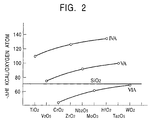
- Fig. 2 shows a comparison of generated heat of IV A metals (Ti, Zr, Hf) and V A metals (V, Nb, Ta) with that of silicon oxides. These metals are characterized in that the amount of heat generated by oxides is smaller than that of silicon. Accordingly, in the event that these are deposited on a silicon oxide, oxides are generated at the interface, and these metal materials strongly bind to the silicon oxide. With the printer head 21, the lower layer of the heat-generating elements 35 is a silicon nitride, but these metals hold the same relation with silicon nitrides, as well.
- the buffer layer 35A strongly binds with the silicone nitride which is the underlayer.
- these metal materials and the tantalum nitride or the like making up the heat-generating elements 30 are metal materials of the same type, so the buffer layer 35A and the resistor layer 35B can also be made to strongly bind.
- the printer head 21 even in the event that thermal stress is repeatedly applied by heating the ink under conditions wherein the linear expansion coefficients of the silicone nitride which is the lower layer and that of the tantalum nitride which is the resistor material greatly differ, the resistor material can be prevented from peeling off of the lower layer, and consequently change in resistance values, and destruction and the like, of the heat-generating elements 35 can be prevented, thereby markedly improving the reliability of the heat-generating elements 35 as compared to the conventional.
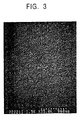
- Fig. 3 is an SEM observation photograph showing the state of the surface of a heat-generating element 35, and by comparison with Figs. 6 and 7 it can be understood that the resistor material is sufficiently adhered to the lower layer, since there are no protrusions or recesses formed whatsoever.
- Fig. 4 shows experiment results of repeating passing pulses as a comparison with conventional heat-generating elements, and the improvement in reliability can be confirmed from these experiment results, as well. Also, this experiment involves applying electric power far greater than that actually applied in usage.
- the reference numeral L1 represents that of the printer head 21 according to the present embodiment
- reference numeral L2 represents that wherein the titanium nitride is positioned directly upon the lower layer, according to the conventional configuration. Incidentally, observing the surface state in the same manner with a SEM following such experimentation did not reveal any change in the printer head according to the present embodiment.
- the reliability of the heat-generating elements can be markedly improved over that of the conventional, by depositing a titanium layer which is a IV A metal layer following which a resistor material is deposited to form heat-generating elements.
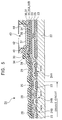
- Fig. 5 is a cross-sectional diagram illustrating a printer head applied to a printer according to a second embodiment of the present invention, as a comparison to Fig. 1.
- configurations which are the same as the printer head described above with reference to Fig. 1 will be denoted with corresponding reference numerals, and redundant description will be omitted.
- the driving circuit for driving the switching transistors 24A is formed by NMOS and PMOS transistors 24B being connected by the first layer of wiring pattern 28. Also, the driving circuit and the switching transistors 24A are connected by this first layer of wiring pattern 28. Subsequently, after the silicon nitride film 34 is deposited, the heat-generating elements 35 are formed, one end of the heat-generating elements 35 and the switching transistors 24A are connected by the second layer of wiring pattern 30, and also the other end of the heat-generating elements 35 is connected to the electric power line. Thus, the order of making the second layer of wiring pattern 30 and the heat-generating elements 35 is reversed with regard to that of the above-described first embodiment.
- the heat-generating elements 35 are formed by depositing a tantalum resistor material 35B following depositing the titanium buffer layer 35A on the silicon nitride film 34 which is the lower layer.
- the resistor material is deposited following depositing of the titanium layer which is a IV A metal layer to form the heat-generating elements, and tantalum is applied for this resistor material.
- the buffer layer is formed of titanium, of the IA A metal materials
- the present invention is not restricted to this, and advantages the same of those of the above-described embodiments can be obtained by forming the buffer layer of other IV A metals such as zirconium or hafnium, and also advantages the same of those of the above-described embodiments can be obtained by forming the buffer layer of V A metal materials instead of IV A metal materials.
- the buffer layer is formed of one layer of a IV A metal material
- the present invention is not restricted to this, and since the essence of the present invention is to prevent change in the properties of the heat-generating elements by improving the binding with the lower layer, advantages the same of those of the above-described embodiments can be obtained by forming the buffer layer of a multi-layer structure wherein a IV A metal film or a V A metal film is positioned at the lower layer side.
- the present invention is not restricted to this, and can be widely applied to various types of printers heads which print by driving heat-generating elements, such as thermo-sensitive printer heads or the like, and further to printers using such printer heads.
- heat-generating elements are formed by depositing at least a IV A metal layer or a V A metal layer, followed by depositing a resistor material thereupon, so the reliability of the heat-generating elements can be improved over the conventional.
Landscapes
- Engineering & Computer Science (AREA)
- Manufacturing & Machinery (AREA)
- Particle Formation And Scattering Control In Inkjet Printers (AREA)
Abstract
Description
Claims (3)
- A printer comprising a heat-generating element on a semiconductor substrate and a transistor for driving said heat-generating element, for printing a desired image by generating heat with said heat-generating element;
wherein said heat-generating element is formed by depositing at least a IV A metal layer or a V A metal layer, followed by depositing a resistor material upon said metal layer. - A printer head comprising a heat-generating element on a semiconductor substrate and a transistor for driving said heat-generating element, for printing a desired image by generating heat with said heat-generating element;
wherein said heat-generating element is formed by depositing at least a IV A metal layer or a V A metal layer, followed by depositing a resistor material upon said metal layer. - A method for manufacturing a printer head comprising a heat-generating element on a semiconductor substrate and a transistor for driving said heat-generating element, for printing a desired image by generating heat with said heat-generating element;
wherein said heat-generating element is formed by depositing at least a IV A metal layer or a V A metal layer, followed by depositing a resistor material upon said metal layer.
Applications Claiming Priority (2)
| Application Number | Priority Date | Filing Date | Title |
|---|---|---|---|
| JP2000243996 | 2000-08-07 | ||
| JP2000243996A JP4654494B2 (en) | 2000-08-07 | 2000-08-07 | Printer, printer head and printer head manufacturing method |
Publications (2)
| Publication Number | Publication Date |
|---|---|
| EP1180434A1 true EP1180434A1 (en) | 2002-02-20 |
| EP1180434B1 EP1180434B1 (en) | 2007-10-10 |
Family
ID=18734756
Family Applications (1)
| Application Number | Title | Priority Date | Filing Date |
|---|---|---|---|
| EP01118990A Expired - Lifetime EP1180434B1 (en) | 2000-08-07 | 2001-08-06 | Printer, printer head, and method for manufacturing printer head |
Country Status (5)
| Country | Link |
|---|---|
| US (1) | US6513912B2 (en) |
| EP (1) | EP1180434B1 (en) |
| JP (1) | JP4654494B2 (en) |
| DE (1) | DE60130842T2 (en) |
| SG (1) | SG99931A1 (en) |
Cited By (6)
| Publication number | Priority date | Publication date | Assignee | Title |
|---|---|---|---|---|
| EP1205303B1 (en) * | 2000-11-07 | 2008-04-16 | Sony Corporation | Printer, printer head, and method of producing the printer head |
| EP2017083A1 (en) * | 2007-07-16 | 2009-01-21 | Samsung Electronics Co., Ltd. | Inkjet Print Head and Manufacturing Method Thereof |
| EP1872949A3 (en) * | 2006-06-27 | 2009-08-05 | Samsung Electronics Co., Ltd. | Print Head and Fabrication Method Thereof |
| EP2075132A3 (en) * | 2007-11-29 | 2009-10-28 | International United Technology Co., Ltd. | Thermal injekt printhead chip structure and manufacturing method for the same |
| US7722168B2 (en) | 2002-11-23 | 2010-05-25 | Silverbrook Research Pty Ltd | Inkjet printhead incorporating coincident groups of ink apertures |
| US7771027B2 (en) | 2002-11-23 | 2010-08-10 | Silverbrook Research Pty Ltd | Self-cooling high nozzle density ink jet nozzle arrangement |
Families Citing this family (4)
| Publication number | Priority date | Publication date | Assignee | Title |
|---|---|---|---|---|
| JP3900349B2 (en) * | 2003-04-04 | 2007-04-04 | ソニー株式会社 | Wireless device and wireless device system |
| KR100571769B1 (en) | 2003-08-25 | 2006-04-18 | 삼성전자주식회사 | A protective layer of the inkjet printhead and a method of manufacturing an inkjet printhead having the same |
| JP5008448B2 (en) * | 2007-04-20 | 2012-08-22 | キヤノン株式会社 | Method for manufacturing substrate for ink jet recording head |
| CN105939857B (en) | 2014-01-29 | 2017-09-26 | 惠普发展公司,有限责任合伙企业 | Hot ink-jet print head |
Citations (3)
| Publication number | Priority date | Publication date | Assignee | Title |
|---|---|---|---|---|
| US5008689A (en) * | 1988-03-16 | 1991-04-16 | Hewlett-Packard Company | Plastic substrate for thermal ink jet printer |
| US5710070A (en) * | 1996-11-08 | 1998-01-20 | Chartered Semiconductor Manufacturing Pte Ltd. | Application of titanium nitride and tungsten nitride thin film resistor for thermal ink jet technology |
| JPH10119284A (en) * | 1996-10-21 | 1998-05-12 | Canon Inc | Inkjet substrate, inkjet head, inkjet pen, and inkjet device |
Family Cites Families (7)
| Publication number | Priority date | Publication date | Assignee | Title |
|---|---|---|---|---|
| JPH02212152A (en) * | 1989-02-14 | 1990-08-23 | Canon Inc | Liquid jet recording head |
| JP2866256B2 (en) * | 1992-06-02 | 1999-03-08 | キヤノン株式会社 | INK JET HEAD, METHOD OF MANUFACTURING THE SAME, AND INK JET RECORDING APPARATUS USING THE SAME |
| JP2727989B2 (en) | 1994-11-25 | 1998-03-18 | 日本電気株式会社 | Manufacturing method of thermal head |
| JPH1170658A (en) * | 1997-06-20 | 1999-03-16 | Canon Inc | Recording element unit, ink jet recording element unit, ink jet cartridge, and ink jet recording apparatus |
| US6109733A (en) * | 1997-11-21 | 2000-08-29 | Xerox Corporation | Printhead for thermal ink jet devices |
| JPH11297942A (en) * | 1998-04-08 | 1999-10-29 | Nec Corp | Ferroelectric memory device and method of manufacturing the same |
| JP2000015817A (en) * | 1998-07-01 | 2000-01-18 | Casio Comput Co Ltd | Inkjet head |
-
2000
- 2000-08-07 JP JP2000243996A patent/JP4654494B2/en not_active Expired - Fee Related
-
2001
- 2001-07-31 US US09/918,836 patent/US6513912B2/en not_active Expired - Lifetime
- 2001-08-06 SG SG200104671A patent/SG99931A1/en unknown
- 2001-08-06 DE DE60130842T patent/DE60130842T2/en not_active Expired - Lifetime
- 2001-08-06 EP EP01118990A patent/EP1180434B1/en not_active Expired - Lifetime
Patent Citations (3)
| Publication number | Priority date | Publication date | Assignee | Title |
|---|---|---|---|---|
| US5008689A (en) * | 1988-03-16 | 1991-04-16 | Hewlett-Packard Company | Plastic substrate for thermal ink jet printer |
| JPH10119284A (en) * | 1996-10-21 | 1998-05-12 | Canon Inc | Inkjet substrate, inkjet head, inkjet pen, and inkjet device |
| US5710070A (en) * | 1996-11-08 | 1998-01-20 | Chartered Semiconductor Manufacturing Pte Ltd. | Application of titanium nitride and tungsten nitride thin film resistor for thermal ink jet technology |
Cited By (19)
| Publication number | Priority date | Publication date | Assignee | Title |
|---|---|---|---|---|
| EP1205303B1 (en) * | 2000-11-07 | 2008-04-16 | Sony Corporation | Printer, printer head, and method of producing the printer head |
| US7988261B2 (en) | 2002-11-23 | 2011-08-02 | Silverbrook Research Pty Ltd | Printhead having layered heater elements and electrodes |
| US8011760B2 (en) | 2002-11-23 | 2011-09-06 | Silverbrook Research Pty Ltd | Inkjet printhead with suspended heater element spaced from chamber walls |
| US8322826B2 (en) | 2002-11-23 | 2012-12-04 | Zamtec Limited | Method of ejecting fluid using wide heater element |
| US7722168B2 (en) | 2002-11-23 | 2010-05-25 | Silverbrook Research Pty Ltd | Inkjet printhead incorporating coincident groups of ink apertures |
| US7771027B2 (en) | 2002-11-23 | 2010-08-10 | Silverbrook Research Pty Ltd | Self-cooling high nozzle density ink jet nozzle arrangement |
| US7971970B2 (en) | 2002-11-23 | 2011-07-05 | Silverbrook Research Pty Ltd | Ink ejection device with circular chamber and concentric heater element |
| US7980673B2 (en) | 2002-11-23 | 2011-07-19 | Silverbrook Research Pty Ltd | Inkjet nozzle assembly with low density suspended heater element |
| US8287097B2 (en) | 2002-11-23 | 2012-10-16 | Zamtec Limited | Inkjet printer utilizing low energy titanium nitride heater elements |
| US8277029B2 (en) | 2002-11-23 | 2012-10-02 | Zamtec Limited | Printhead integrated circuit having low mass heater elements |
| US7997688B2 (en) | 2002-11-23 | 2011-08-16 | Silverbrook Research Pty Ltd | Unit cell for thermal inkjet printhead |
| US8007075B2 (en) | 2002-11-23 | 2011-08-30 | Silverbrook Research Pty Ltd | Printhead having nozzle plate formed on fluid distributors |
| US8075111B2 (en) | 2002-11-23 | 2011-12-13 | Silverbrook Research Pty Ltd | Printhead with ink distribution through aligned apertures |
| US8087751B2 (en) | 2002-11-23 | 2012-01-03 | Silverbrook Research Pty Ltd | Thermal ink jet printhead |
| US8118407B2 (en) | 2002-11-23 | 2012-02-21 | Silverbrook Research Pty Ltd | Thermal inkjet printhead having annulus shaped heater elements |
| EP1872949A3 (en) * | 2006-06-27 | 2009-08-05 | Samsung Electronics Co., Ltd. | Print Head and Fabrication Method Thereof |
| EP2017083A1 (en) * | 2007-07-16 | 2009-01-21 | Samsung Electronics Co., Ltd. | Inkjet Print Head and Manufacturing Method Thereof |
| EP2075132A3 (en) * | 2007-11-29 | 2009-10-28 | International United Technology Co., Ltd. | Thermal injekt printhead chip structure and manufacturing method for the same |
| US8376524B2 (en) | 2007-11-29 | 2013-02-19 | International United Technology Company, Ltd. | Thermal inkjet printhead chip structure and manufacturing method for the same |
Also Published As
| Publication number | Publication date |
|---|---|
| JP4654494B2 (en) | 2011-03-23 |
| US6513912B2 (en) | 2003-02-04 |
| JP2002052724A (en) | 2002-02-19 |
| EP1180434B1 (en) | 2007-10-10 |
| US20020057314A1 (en) | 2002-05-16 |
| DE60130842D1 (en) | 2007-11-22 |
| DE60130842T2 (en) | 2008-07-17 |
| SG99931A1 (en) | 2003-11-27 |
Similar Documents
| Publication | Publication Date | Title |
|---|---|---|
| US6513912B2 (en) | Heat generating element for printer head and manufacturing method therefor | |
| US6848770B2 (en) | Liquid dispenser and printer | |
| EP1205303B1 (en) | Printer, printer head, and method of producing the printer head | |
| US6536877B2 (en) | Printer, printer head, and method for fabricating printer head formed with a multilayer wiring pattern | |
| JP3937804B2 (en) | Method for manufacturing structure having through hole | |
| EP1205304B1 (en) | Printer, printer head, and method of producing the printer head | |
| KR100866270B1 (en) | Manufacturing method of liquid jet head, liquid jet device and liquid jet head | |
| US20030080359A1 (en) | Structure with through hole, production method thereof, and liquid discharge head | |
| US6773091B2 (en) | Liquid discharge device and method of manufacturing the same | |
| WO2005021267A1 (en) | Liquid discharge head, liquid discharge device, and method for manufacturing liquid discharge head | |
| JP2002307684A (en) | Printer, printer head, and method of manufacturing printer head | |
| JP2001212995A (en) | Printers and printer heads | |
| JP2003019799A (en) | Printer head, printer and method of manufacturing printer head | |
| JP2003291353A (en) | Liquid ejector, printer and method for manufacturing liquid ejector | |
| JP2004276380A (en) | Method for forming liquid ejection head and method for forming film | |
| JP2003127377A (en) | Printer head, printer and method of manufacturing printer head | |
| JP2004017567A (en) | Liquid discharge head, liquid discharge device, and method of manufacturing liquid discharge head |
Legal Events
| Date | Code | Title | Description |
|---|---|---|---|
| PUAI | Public reference made under article 153(3) epc to a published international application that has entered the european phase |
Free format text: ORIGINAL CODE: 0009012 |
|
| AK | Designated contracting states |
Kind code of ref document: A1 Designated state(s): AT BE CH CY DE DK ES FI FR GB GR IE IT LI LU MC NL PT SE TR |
|
| AX | Request for extension of the european patent |
Free format text: AL;LT;LV;MK;RO;SI |
|
| 17P | Request for examination filed |
Effective date: 20020722 |
|
| AKX | Designation fees paid |
Free format text: DE FR GB IT |
|
| 17Q | First examination report despatched |
Effective date: 20050415 |
|
| GRAP | Despatch of communication of intention to grant a patent |
Free format text: ORIGINAL CODE: EPIDOSNIGR1 |
|
| GRAS | Grant fee paid |
Free format text: ORIGINAL CODE: EPIDOSNIGR3 |
|
| GRAA | (expected) grant |
Free format text: ORIGINAL CODE: 0009210 |
|
| AK | Designated contracting states |
Kind code of ref document: B1 Designated state(s): DE FR GB IT |
|
| REG | Reference to a national code |
Ref country code: GB Ref legal event code: FG4D |
|
| REF | Corresponds to: |
Ref document number: 60130842 Country of ref document: DE Date of ref document: 20071122 Kind code of ref document: P |
|
| ET | Fr: translation filed | ||
| PLBE | No opposition filed within time limit |
Free format text: ORIGINAL CODE: 0009261 |
|
| STAA | Information on the status of an ep patent application or granted ep patent |
Free format text: STATUS: NO OPPOSITION FILED WITHIN TIME LIMIT |
|
| 26N | No opposition filed |
Effective date: 20080711 |
|
| REG | Reference to a national code |
Ref country code: GB Ref legal event code: 746 Effective date: 20091130 |
|
| PGFP | Annual fee paid to national office [announced via postgrant information from national office to epo] |
Ref country code: GB Payment date: 20120821 Year of fee payment: 12 |
|
| PGFP | Annual fee paid to national office [announced via postgrant information from national office to epo] |
Ref country code: IT Payment date: 20120822 Year of fee payment: 12 Ref country code: FR Payment date: 20120906 Year of fee payment: 12 Ref country code: DE Payment date: 20120822 Year of fee payment: 12 |
|
| GBPC | Gb: european patent ceased through non-payment of renewal fee |
Effective date: 20130806 |
|
| PG25 | Lapsed in a contracting state [announced via postgrant information from national office to epo] |
Ref country code: DE Free format text: LAPSE BECAUSE OF NON-PAYMENT OF DUE FEES Effective date: 20140301 |
|
| REG | Reference to a national code |
Ref country code: DE Ref legal event code: R119 Ref document number: 60130842 Country of ref document: DE Effective date: 20140301 |
|
| REG | Reference to a national code |
Ref country code: FR Ref legal event code: ST Effective date: 20140430 |
|
| PG25 | Lapsed in a contracting state [announced via postgrant information from national office to epo] |
Ref country code: IT Free format text: LAPSE BECAUSE OF NON-PAYMENT OF DUE FEES Effective date: 20130806 |
|
| PG25 | Lapsed in a contracting state [announced via postgrant information from national office to epo] |
Ref country code: GB Free format text: LAPSE BECAUSE OF NON-PAYMENT OF DUE FEES Effective date: 20130806 |
|
| PG25 | Lapsed in a contracting state [announced via postgrant information from national office to epo] |
Ref country code: FR Free format text: LAPSE BECAUSE OF NON-PAYMENT OF DUE FEES Effective date: 20130902 |