Technical Field
The present invention relates to a radio
communication apparatus and radio communication method
for use in a digital communication system, and more
particularly to a radio communication apparatus and
radio communication method that perform radio
communications with a combination of a multicarrier
modulation method such as the OFDM (Orthogonal Frequency
Division Multiplexing) modulation method, and a CDMA
(Code Division Multiple Access) method.
Background Art
Nowadays, in radio communications, and especially
in mobile communications, various kinds of information
such as images and data are transmitted as well as voice.
Henceforth, demand for the transmission of various kinds
of content is expected to continue to grow, further
increasing the necessity of highly reliable, high-speed
transmission. However, when high-speed transmission is
carried out in mobile communications, the effect of
delayed waves due to multipath propagation can no longer
be ignored, and transmission characteristics degrade due
to frequency selective fading.
Multicarrier modulation methods such as the OFDM
modulation method are drawing attention as one kind of
technology for combating frequency selective fading. A
multicarrier modulation method is a technology for
effectively performing high-speed transmission by
transmitting data using a plurality of carriers
(subcarriers) whose speed is suppressed to a level at
which frequency selective fading does not occur. With
the OFDM modulation method, in particular, the
subcarriers on which data is placed are mutually
orthogonal, making this the multicarrier modulation
method offering the highest spectral efficiency.
Moreover, the OFDM modulation method can be implemented
with a comparatively simple hardware configuration.
For these reasons, various studies are being undertaken
concerning the OFDM modulation method as a frequency
selective fading countermeasure.
Also, a spread spectrum method is another
technology for combating frequency selective fading. A
spread spectrum method is a technology that improves
interference immunity by spreading a signal along the
frequency axis by means of a spreading code called a PN
code to obtain spreading gain. Spread spectrum methods
include a direct spreading method and a frequency hopping
method. Of these, a CDMA (Code Division Multiple Access )
method using direct spreading has been decided on for
use in the next-generation mobile communication system
IMT-2000.
OFDM-CDMA methods combining the OFDM modulation
method and CDMA method have recently been a focus of
attention. OFDM-CDMA methods are broadly divided into
time domain spreading and frequency domain spreading.
Time domain spreading and frequency domain spreading
methods are described below.
First, time domain spreading will be described.
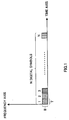
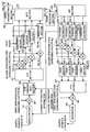
FIG.1 is a diagram showing the state of digital symbols
before modulation processing, and FIG.2 is a diagram
showing the chip arrangement after modulation processing
using the time domain spreading method. With time domain
spreading, N digital symbols (serial data stream)
(FIG.1) are converted to parallel data streams, and then
each digital symbol is multiplied by a spreading code
with spreading factor M. After spreading, chips undergo
sequential inverse fast Fourier transform (IFFT)
processing one chip at a time with N chips in parallel.
As a result, M OFDM symbols with N subcarriers are
generated. That is, with time domain spreading, after
spreading, chips are arranged in time series on the
respective subcarriers (FIG.2).
Assuming that one digital symbol prior to
modulation processing uses radio resources of time width
T and frequency band width B (FIG.1), after modulation
processing, one chip will use time width N×T/M and
frequency band width M×B/N. Therefore, the area
occupied by each digital symbol in the time-frequency
domain is M×T×B, M times the area occupied by one digital
symbol prior to modulation processing.
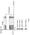
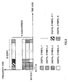
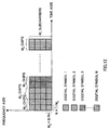
If, for example, number of digital symbols N = 8,
and spreading factor M = 8, the OFDM symbol signal pattern
generated by the time domain spreading method is as shown
in FIG.3. As shown in this diagram, with the time domain
spreading method, eight digital symbols differentiated
by black-and-white shading on the frequency axis are
assigned sequentially, one chip at a time, each to a
different one of subcarriers f1 through f8, and eight
OFDM symbols are generated at t0 through t7.
Next, frequency domain spreading will be described.
FIG.4 is a diagram showing the arrangement of chips after
modulation processing using the frequency domain
spreading method. With frequency domain spreading, a
serial data stream comprising N digital symbols (serial
data stream) (FIG. 1) are multiplied, one symbol at a time,
by a spreading code with spreading factor M. After
spreading, chips undergo sequential IFFT processing one
symbol at a time with M chips in parallel. As a result,
N OFDM symbols with M subcarriers are generated. That
is, with frequency domain spreading, after spreading,
chips are arranged along the frequency axis at their
respective times (FIG.4). In other words, after
spreading, chips are arranged on different subcarriers.
Assuming that one digital symbol prior to
modulation processing uses radio resources of time width
T and frequency band width B (FIG.1), as described above,
after modulation processing, one chip will use time width
N×T and frequency band width B/N. Therefore, the area
occupied by each digital symbol in the time-frequency
domain is M×T×B, as with time domain spreading, M times
the area occupied by one digital symbol prior to
modulation processing.
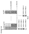
If, for example, number of digital symbols N = 8,
and spreading factor M = 8, the OFDM symbol signal pattern
generated by the frequency domain spreading method is
as shown in FIG.5. As shown in this diagram, with the
frequency domain spreading method, eight OFDM symbols
are generated sequentially at t0 through t7 for eight
digital symbols differentiated by black-and-white
shading on the time axis. At this time, the eight chips
for each digital symbol are assigned each to a different
one of subcarriers f1 through f8.
By using a time domain spreading method or frequency
domain spreading method as described above, it is
possible to achieve efficient reuse and obtain a
statistical multiplexing effect. Moreover, faster data
transmission can be achieved than with single-carrier
CDMA. Reuse is the ability to use the same frequency in
an adjacent cell. A statistical multiplexing effect is
the ability to accommodate more user signals when data
presence occurs randomly according to the user than in
the case of continuous transmission according to a
decrease in energy in an interval in which there is no
reciprocal transmission.
However, with the time domain spreading method, if
a particular digital symbol is considered, since a
plurality of post-spreading chips are arranged in a time
series at the same frequency (FIG.2 and FIG.3), multipath
separation is possible and a path diversity effect is
obtained, but a frequency diversity effect is not
obtained. Therefore, if transmission power control is
imperfect due to radio channel conditions, transmission
characteristics degrade precipitously. Also, even when
transmission power control is performed perfectly, the
resulting increase in the transmission power causes
problems such as greater battery consumption at a mobile
station apparatus, larger amplifier size, and greater
interference with other cells.
Also, with the frequency domain spreading method,
if a particular digital symbol is considered, since a
plurality of post-spreading chips are arranged on
different subcarriers at the same time (FIG.4 and FIG.5),
a frequency diversity effect is obtained, but path
separation is not possible and a path diversity effect
is not obtained. As RAKE combination can therefore not
be used, it is not possible to reduce multipath
distortion. Also, if a plurality of user signals are
code division multiplexed on each subcarrier, even if
orthogonal codes are used in spreading processing,
orthogonality cannot be maintained because of the
influence of multipath distortion, and therefore the
level of code division multiplexing is limited.
Moreover, the influence of signal extraction timing
variations in a Fourier transform is increased.
Disclosure of Invention
It is an object of the present invention to provide
a radio communication apparatus and radio communication
method that enable both a frequency diversity effect and
a path diversity effect to be obtained, and transmission
characteristics to be improved compared with heretofore,
in radio communications in which a multicarrier
modulation method and CDMA method are combined.
In order to achieve the above object, in the present
invention, in radio communications in which a
multicarrier modulation method and CDMA method are
combined, a plurality of chips after spreading of a
particular digital symbol that are conventionally
arranged one-dimensionally, aligned either on the
frequency axis or on the time axis, are arranged
two-dimensionally, distributed both on the frequency
axis and on the time axis. By this means, it is possible
to obtain both a frequency diversity effect and a path
diversity effect in radio communications in which a
multicarrier modulation method and CDMA method are
combined.
Brief Description of Drawings
FIG.1 is a diagram showing the state of digital
symbols before modulation processing;
FIG.2 is a diagram showing the chip arrangement with
a conventional time domain spreading method;
FIG.3 is a diagram of an OFDM symbol signal pattern
with a conventional time domain spreading method;
FIG. 4 is a diagram showing the chip arrangement with
a conventional frequency domain spreading method;
FIG.5 is a diagram of an OFDM symbol signal pattern
with a conventional frequency domain spreading method;
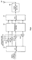
FIG.6 is a block diagram showing the configuration
of the transmitting side in a radio communication
apparatus according to Embodiment 1 of the present
invention;
FIG.7 is a block diagram showing the configuration
of the receiving side in a radio communication apparatus
according to Embodiment 1 of the present invention;
FIG.8 is a diagram showing the chip arrangement of
a radio communication apparatus according to Embodiment
1 of the present invention;
FIG.9 is a diagram of an OFDM symbol signal pattern
transmitted from a radio communication apparatus .
according to Embodiment 1 of the present invention;
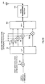
FIG. 10 is a block diagram showing the configuration
of the transmitting side in a radio communication
apparatus according to Embodiment 2 of the present
invention;
FIG. 11 is a block diagram showing the configuration
of the receiving side in a radio communication apparatus
according to Embodiment 2 of the present invention;
FIG.12 is a diagram showing the chip arrangement
of a radio communication apparatus according to
Embodiment 2 of the present invention;
FIG.13 is a diagram of an OFDM symbol signal pattern
transmitted from a radio communication apparatus
according to Embodiment 2 of the present invention;
FIG.14 is a diagram showing the chip arrangement
of a radio communication apparatus according to
Embodiment 2 of the present invention;
FIG. 15 is a diagram of an OFDM symbol signal pattern
transmitted from a radio communication apparatus
according to Embodiment 2 of the present invention;
FIG.16 is a diagram of an OFDM symbol signal pattern
transmitted from a radio communication apparatus
according to Embodiment 2 of the present invention;
FIG.17 is a block diagram showing the configuration
of the transmitting side in a radio communication
apparatus according to Embodiment 3 of the present
invention;
FIG.18 is a block diagram showing the configuration
of the receiving side in a radio communication apparatus
according to Embodiment 3 of the present invention;
FIG. 19 is a diagram of an OFDM symbol signal pattern
transmitted from a radio communication apparatus
according to Embodiment 3 of the present invention;
FIG.20 is a block diagram showing the configuration
of the transmitting side in a radio communication
apparatus according to Embodiment 4 of the present
invention;
FIG.21 is a block diagram showing the configuration
of the receiving side in a radio communication apparatus
according to Embodiment 4 of the present invention;
FIG.22 is a diagram of an OFDM symbol signal pattern
transmitted from a radio communication apparatus
according to Embodiment 4 of the present invention;
FIG.23 is a block diagram showing the configuration
of a radio communication apparatus according to
Embodiment 5 of the present invention; and
FIG.24 is a block diagram showing the configuration
of a radio communication apparatus according to
Embodiment 6 of the present invention.
Best Mode for Carrying out the Invention
With reference now to the accompanying drawings,
embodiments of the present invention will be explained
in detail below. The following descriptions take the
OFDM modulation method as an example of a multicarrier
modulation method. That is, a case is described in which
the transmitted multicarrier signal is OFDM symbol.
(Embodiment 1)
In this embodiment, a particular data item is
arranged two-dimensionally, distributed both on the
frequency axis and on the time axis, by spreading data
on the time axis, and shifting each post-spreading chip
step-wise in the carrier frequency upward or downward
direction on the frequency axis, changing the
arrangement.
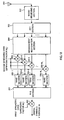
FIG.6 is a block diagram showing the configuration
of the transmitting side in a radio communication
apparatus according to Embodiment 1 of the present
invention. The transmitting side radio communication
apparatus shown in FIG.6 comprises a serial/parallel
conversion section (S/P section) 101, time domain
spreaders 102-1 through 102-N, rearranging section 103,
inverse fast Fourier transform section (IFFT section)
104, radio transmitting section 105, and antenna 106.
FIG.7 is a block diagram showing the configuration
of the receiving side in a radio communication apparatus
according to Embodiment 1 of the present invention. The
receiving side radio communication apparatus shown in
FIG.7 comprises an antenna 201, radio receiving section
202, Fourier transform section (FFT section) 203,
arrangement restoration section 204, time domain
despreaders 205-1 through 205-N, RAKE sections 206-1
through 206-N, and parallel/serial conversion section
(P/S section) 207.
The following description refers to a case where
N digital symbols are transmitted in parallel.
Therefore, the radio communication apparatus shown in
FIG.6 is provided with N time domain spreaders, and the
radio communication apparatus shown in FIG.7 is provided
with N time domain despreaders and RAKE sections.
First, in the transmitting side radio
communication apparatus shown in FIG.6, N digital
symbols 1 through N (serial data stream) shown in FIG.1
are converted to parallel data streams by the S/P section
101, and each of these is input to the corresponding time
domain spreader. That is, digital symbol 1 is input to
time domain spreader 102-1, digital symbol 2 is input
to time domain spreader 102-2, and so on through to
digital symbol N which is input to time domain spreader
102-N.
In time domain spreaders 102-1 through 102-N,
digital symbols 1 through N are spread by means of a
spreading code with spreading factor M. That is, digital
symbols 1 through N are spread to M chips on the time
axis. More specifically, digital symbol 1 is spread to
t0 through tM time chips by time domain spreader 102-1,
digital symbol 2 is spread to t0 through tM time chips
by time domain spreader 102-2, and so on through to
digital symbol N which is spread to t0 through tM time
chips by time domain spreader 102-N. The post-spreading
data of M chips is input to the rearranging section 103.
Thus, chip arrangement data is stored in the rearranging
section 103 as shown in FIG.2. That is, data of N symbols
is stored in the frequency axis direction, and data of
M chips is stored in the time axis direction.
In the rearranging section 103, each post-spreading
chip undergoes rearrangement by being shifted
step-wise in the carrier frequency upward or downward
direction on the frequency axis. Here, digital symbol
1 will be considered, taking the case where a shift is
made in the carrier frequency upward direction. That is,
chips 1 through M of digital symbol 1 spread in the time
axis direction are shifted one step at a time in the
carrier frequency upward direction as shown in FIG.8.
This kind of shift processing is carried out on chips
1 through M of digital symbols 1 through N.
After rearrangement, chips are input sequentially
to the IFFT section 104 with N in parallel, and undergo
IFFT processing. As a result of performing IFFT
processing after rearrangement has been performed in
this way, first, OFDM symbols are generated with chip
1 of digital symbol 1 assigned to subcarrier 1, chip 1
of digital symbol 2 assigned to subcarrier 2, and so on
through to chip 1 of digital symbol N which is assigned
to subcarrier N, and then OFDM symbols are generated with
chip 2 of digital symbol N assigned to subcarrier 1, chip
2 of digital symbol 1 assigned to subcarrier 2, and so
on through to chip 2 of digital symbol N-1 which is
assigned to subcarrier N. M such OFDM symbols are
generated. That is, a particular digital symbol is
arranged two-dimensionally, distributed both on the
frequency axis and on the time axis.
If, for example, number of digital symbols N = 8,
and spreading factor M = 8, the OFDM symbol signal pattern
generated by the IFFT section 104 is as shown in FIG.9.
As shown in this diagram, in this embodiment, eight
digital symbols differentiated by black-and-white
shading are assigned sequentially, with the elapse of
time, one chip at a time, each to a different one of
subcarriers f1 through f8, and eight OFDM symbols are
generated at t0 through t7. That is, the eight chips into
which digital symbol 1 is spread are arranged
respectively at time t0 of frequency f1, time t1 of
frequency f2, time t2 of frequency f3, time t3 of
frequency f4, time t4 of frequency f5, time t5 of
frequency f6, time t6 of frequency f7, and time t7 of
frequency f8.
Similarly, each chip of digital symbols 2 through
8, also, is arranged step-wise ahead of digital symbol
1. For example, the chips of digital symbol 2 are
arranged at time t0 of frequency f2, time t1 of frequency
f3, time t2 of frequency f4, time t3 of frequency f5,
time t4 of frequency f6, time t5 of frequency f7, and
time t6 of frequency f8.
As shown in FIG.8, one chip uses a time width of
N×T/M and a frequency band width of M×B/N. That is, the
interval between subcarriers in OFDM symbol shown in
FIG.9 is M×B/N. Therefore, the area occupied by each
digital symbol in the time-frequency domain is M×T×B,
M times the area occupied by one digital symbol prior
to modulation processing.
M OFDM symbols generated by the IFFT section 104
are input sequentially to the radio transmitting section
105, and after undergoing predetermined radio processing
such as up-conversion, are transmitted from the antenna
106.
In the receiving side radio communication
apparatus shown in FIG.7, predetermined radio processing
such as down-conversion is carried out by the radio
receiving section 202 on OFDM symbols received via the
antenna 201. After undergoing the predetermined radio
processing, OFDM symbols are input to the FFT section
203. Signals of digital symbols 1 through N transmitted
by means of subcarriers 1 through N are then extracted
by having FFT processing performed on the OFDM symbols
by the FFT section 203. Similar processing is performed
for M OFDM symbols received sequentially, and the
resulting signals are input to the arrangement
restoration section 204.
The arrangement restoration section 204 performs
rearrangement that is the reverse of the rearrangement
performed by the rearranging section 103 in the
transmitting side radio communication apparatus. By
this means, the arrangement of chips is restored to what
it was prior to rearrangement by the rearranging section
103. That is, the arrangement of chips is restored to
the arrangement shown in FIG.2. After their arrangement
has been restored, the chips are input, N in parallel,
to time domain despreaders 205-1 through 205-N and
despread. After despreading, the data streams are input
to RAKE sections 206-1 through 206-N, respectively.
RAKE sections 206-1 through 206-N perform RAKE
combination processing that gathers together and
combines delay path components along the time axis . That
is, RAKE combination for digital symbol 1 is performed
by RAKE section 206-1, RAKE combination for digital
symbol 2 is performed by RAKE section 206-2, and so on
through to RAKE combination for digital symbol N
performed by RAKE section 206-N. After RAKE combination,
digital symbols are input to the P/S section 207.
In the P/S section 207, digital symbols 1 through
N that were input in parallel from RAKE sections 206-1
through 206-N are converted to a serial data stream and
output. By this means, RAKE-combined digital symbols 1
through N are obtained sequentially.
Thus, in this embodiment, on the transmitting side,
data (digital symbols) assigned to a plurality of
subcarriers of different frequencies by means of S/P
conversion are spread in the time elapse direction, and
post-spreading chips are shifted step-wise in the
carrier frequency upward or downward direction on the
frequency axis, changing the arrangement, after which
OFDM symbols are generated by IFFT processing. Also, on
the receiving side, data that has undergone FFT
processing is restored to its arrangement prior to being
rearranged on the transmitting side, and this restored
data is despread in the time elapse direction.
By this means, each item of data after despreading
includes a plurality of components with different times
and different frequencies. Thus, since a plurality of
components with different frequencies are included, a
frequency diversity effect is obtained. And since, at
the same time, a plurality of components with different
times are included, multipath separation is possible at
OFDM symbol precision, and consequently RAKE combination
is possible, enabling multipath distortion to be reduced.
That is to say, a path diversity effect is obtained. Also,
it is possible to increase the level of code division
multiplexing to enable orthogonality to be maintained
when orthogonal codes are used in spreading processing.
Moreover, the influence of variations in signal
extraction timing in Fourier transform processing can
be suppressed.
Furthermore, high-speed transmission power
control is not necessary, and transmission power control
precision and reflection time can be made less stringent.
As a result, the precipitance of characteristic
degradation when transmission power control is imperfect,
which has heretofore been a problem, can be alleviated.
Moreover, it is possible to mitigate increase of battery
consumption in mobile station apparatus, increase of
amplifier size, increase of interference with other
cells, and so forth, resulting from an increase in
transmission power due to transmission power control.
In this embodiment, a particular digital symbol is
arranged two-dimensionally, distributed both on the
frequency axis and on the time axis, by having each chip
that has been spread on the time axis shifted step-wise
in the carrier frequency upward or downward direction
on the frequency axis. However, in this embodiment, the
method of distribution on the frequency axis is not
limited to this, and any distribution method may be used
as long as it is a method of distribution on the frequency
axis based on a predetermined rule.
(Embodiment 2)
In this embodiment, a particular data item is
arranged two-dimensionally, distributed both on the
frequency axis and on the time axis, by spreading data
in both the frequency domain and time domain-that is,
by spreading data in both the frequency axis direction
and time axis direction.
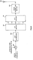
FIG. 10 is a block diagram showing the configuration
of the transmitting side in a radio communication
apparatus according to Embodiment 2 of the present
invention. The transmitting side radio communication
apparatus shown in FIG.10 comprises a frequency domain
spreader 301, S/P section 101, time domain spreaders
102-1 through 102-M1, IFFT section 104, radio
transmitting section 105, and antenna 106. Parts in
FIG.10 identical to those in Embodiment 1 (FIG.6) are
assigned the same codes as in FIG.6 and their detailed
explanations are omitted.
FIG.11 is a block diagram showing the configuration
of the receiving side in a radio communication apparatus
according to Embodiment 2 of the present invention. The
receiving side radio communication apparatus shown in
FIG.11 comprises an antenna 201, radio receiving section
202, FFT section 203, time domain despreaders 205-1
through 205-M1, RAKE sections 206-1 through 206-M1, P/S
section 207, and frequency domain despreader 401. Parts
in FIG.11 identical to those in Embodiment 1 (FIG.7) are
assigned the same codes as in FIG.7 and their detailed
explanations are omitted.
The following description refers to a case where
1 through N digital symbols are spread on the frequency
axis with spreading factor M1. Therefore, the radio
communication apparatus shown in FIG.10 is provided with
M1 time domain spreaders, and the radio communication
apparatus shown in FIG. 11 is provided with M1 time domain
despreaders and RAKE sections.
First, in the transmitting side radio
communication apparatus shown in FIG.10, N digital
symbols 1 through N (serial data stream) shown in FIG.1
are spread by the frequency domain spreader 301 by means
of a first spreading code with spreading factor M1. The
post-spreading data of M1 chips is input to the S/P
section 101. In the S/P section 101, data of M1 chips
input serially is converted to parallel data. By this
processing, digital symbols 1 through N are spread to
M1 chips on the frequency axis, and as a result, chips
1 through M1 are assigned to subcarriers 1 through M1,
respectively, each of a different frequency.
The M1 chips converted to parallel form by the S/P
section 101 are input to the respective corresponding
time domain spreaders. That is, the first chip of each
digital symbol is input to time domain spreader 102-1,
the second chip is input to time domain spreader 102-2,
and so on through to the M1'th chip which is input to time
domain spreader 102-M1.
In time domain spreaders 102-1 through 102-M1,
chips 1 through M1 are further spread by means of a second
spreading code with spreading factor M2. That is, the
digital symbols spread to M1 chips on the frequency axis
are further spread to M2 chips on the time axis. In other
words, each digital symbol is spread by M1×M2 times, that
is, M1 times in the frequency domain and M2 times in the
time domain. By this means, a particular digital symbol
is arranged two-dimensionally, distributed both on the
frequency axis and on the time axis. Chips spread by time
domain spreaders 102-1 through 102-M1 are input
sequentially to the IFFT section 104, M1 in parallel, and
undergo IFFT processing. As a result, N×M2 OFDM symbols
are generated by the IFFT section 104.
For example, if frequency domain spreading factor
M1 = 4 and time domain spreading factor M2 = 2, the chip
arrangement on the frequency axis and time axis is as
shown in FIG.12. That is, digital symbols 1 through N
are arranged sequentially for four chips in the frequency
axis direction and for two chips in the time axis
direction.
Also, the OFDM symbol signal pattern generated by
the IFFT section 104 is as shown in FIG.13. That is, the
eight chips into which digital symbol 1 is spread are
arranged respectively at time t0 of frequency f1, time
t0 of frequency f2, time t0 of frequency f3, time t0 of
frequency f4, time t1 of frequency f1, time t1 of
frequency f2, time t1 of frequency f3, and time t1 of
frequency f4. Similarly, each chip of digital symbols
2 through 8, also, is arranged after digital symbol 1.
For example, the chips of digital symbol 2 are arranged
at time t2 of frequency f1, time t2 of frequency f2, time
t2 of frequency f3, time t2 of frequency f4, time t3 of
frequency f1, time t3 of frequency f2, time t3 of
frequency f3, and time t3 of frequency f4.
As shown in FIG.12, one chip uses a time width of
N×T/M2 and a frequency band width of M2×B/N. That is,
the interval between subcarriers in OFDM symbol shown
in FIG. 13 is M2×B/N. Therefore, the area occupied by each
digital symbol in the time-frequency domain is M1×M2×T×B,
M1×M2 times the area occupied by one digital symbol prior
to modulation processing. Also, if M1×M2=M, the
spreading factor in this embodiment is M times, as in
Embodiment 1.
In the receiving side radio communication
apparatus shown in FIG.11, after undergoing radio
processing, OFDM symbols are input to the FFT section
203. Signals transmitted by means of subcarriers 1
through M1 are then extracted by having FFT processing
performed on the OFDM symbols by the FFT section 203.
Similar processing is performed for N×M2 OFDM symbols
received sequentially, and the resulting signals are
input to time domain despreaders 205-1 through 205-M1.
In time domain despreaders 205-1 through 205-M1,
despreading processing is carried out on the input data
by means of the same second spreading code (spreading
factor M2) used by time domain spreaders 102-1 through
102-M1 in the transmitting side radio communication
apparatus. That is, despreading processing is
performed in the time domain. After despreading, the
data is RAKE-combined by RAKE sections 206-1 through
206-M1, and then converted to a serial data stream by the
P/S section 207 and input to the frequency domain
despreader 401.
In the frequency domain despreader 401,
despreading processing is carried out on the input data
by means of the same first spreading code (spreading
factor M1) used by the frequency domain spreader 301 in
the transmitting side radio communication apparatus.
By this means, RAKE-combined digital symbols 1 through
N are obtained sequentially.
In this embodiment, it is also possible to perform
parallel transmission of X digital symbols. In this case,
the number of time domain spreaders required in the
transmitting side radio communication apparatus, and the
number of time domain despreaders and RAKE sections
required in the receiving side radio communication
apparatus, is X×M1. That is, X×M1 subcarriers are
included in one OFDM symbol.
For example, if two digital symbols are transmitted
in parallel, the S/P section in the transmitting side
radio communication apparatus outputs in parallel chips
of digital symbol 1 and digital symbol 2 spread M1 times
respectively. That is to say, 2×M1 chips are output in
parallel. As a result, digital symbol 1 and digital
symbol 2 are simultaneously spread to M1 chips each on
the frequency axis. Then each chip is further spread to
M2 chips on the time axis by a time domain spreader 102.
Therefore, if, for example, frequency domain
spreading factor M1 = 4 and time domain spreading factor
M2 = 2, the chip arrangement on the frequency axis and
time axis is as shown in FIG.14. That is, digital symbols
spread to 4×2 chips are arranged in parallel two digital
symbols at a time on the frequency axis.
Also, the OFDM symbol signal pattern generated by
the IFFT section 104 is as shown in FIG.15. That is, the
eight chips into which digital symbol 1 is spread are
arranged respectively at time t0 of frequency f1, time
t0 of frequency f2, time t0 of frequency f3, time t0 of
frequency f4, time t1 of frequency f5, time t1 of
frequency f6, time t1 of frequency f7, and time t1 of
frequency f8. And the chips of digital symbol 2 are
arranged at time t0 of frequency f5, time t0 of frequency
f6, time t0 of frequency f7, time t0 of frequency f8,
time t1 of frequency f5, time t1 of frequency f6, time
t1 of frequency f7, and time t1 of frequency f8.
Thus, in this embodiment, on the transmitting side,
data (digital symbols) are spread in both the frequency
domain and time domain, after which OFDM symbols are
generated by IFFT processing. Also, on the receiving
side, despreading is performed in both the frequency
domain and time domain corresponding to spreading
processing on the transmitting side. By this means, the
same kind of effect is obtained as with Embodiment 1.
Also, in this embodiment, it is possible to perform
spreading in the time axis direction individually for
each of frequencies f1 through f8, or to form groups of
close frequencies and perform this spreading
individually for each group. For instance, by grouping
f1, f3, f5, and f7 into one group, and f2, f4, f6, and
f8 into one group, and performing spreading in the time
axis direction for each group, the same digital symbol
occurs twice in succession in the time axis direction,
and occurs in alternating fashion in the frequency axis
direction, as shown in FIG. 16, for example. In this way,
it is possible to maintain the effect of reduced
inter-code interference when using orthogonal codes for
spreading. Moreover, the greater the separation of the
frequencies of the carriers on which the same digital
symbol is arranged, the higher is the frequency diversity
effect, and the nearer frequencies are made to approach,
the greater is the effect of reduced inter-code
interference.
In this embodiment, time domain spreading
processing is performed after frequency domain spreading
processing. However, this order may be reversed. That
is to say, a particular digital symbol can still be
arranged two-dimensionally, distributed on the
frequency axis and time axis, if frequency domain
spreading processing is performed after time domain
spreading processing.
(Embodiment 3)
In this embodiment, after data has been spread in
both the frequency domain and time domain, post-spreading
chips are further shifted step-wise in the
carrier frequency upward or downward direction on the
frequency axis, changing the arrangement.
FIG.17 is a block diagram showing the configuration
of the transmitting side in a radio communication
apparatus according to Embodiment 3 of the present
invention. The transmitting side radio communication
apparatus shown in FIG.17 is configured with the further
provision of a rearranging section 103 as described in
Embodiment 1 between time domain spreaders 102-1 through
102-M1 and IFFT section 104 of a radio communication
apparatus according to Embodiment 2 (FIG.10). Parts in
FIG.17 identical to those in Embodiment 1 (FIG.6) or
Embodiment 2 (FIG.10) are assigned the same codes as in
FIG.6 or FIG.10 and their detailed explanations are
omitted.
FIG.18 is a block diagram showing the configuration
of the receiving side in a radio communication apparatus
according to Embodiment 3 of the present invention. The
receiving side radio communication apparatus shown in
FIG.18 is configured with the further provision of an
arrangement restoration section 204 as described in
Embodiment 1 between the FFT section 203 and time domain
despreaders 205-1 through 205-M1 of a radio communication
apparatus according to Embodiment 2 (FIG.11). Parts in
FIG.18 identical to those in Embodiment 1 (FIG.7) or
Embodiment 2 (FIG.11) are assigned the same codes as in
FIG.7 or FIG.11 and their detailed explanations are
omitted.
In the transmitting side radio communication
apparatus shown in FIG.17, digital symbols are spread
in both the frequency domain and time domain, as
described in Embodiment 2, and further, chips are
rearranged by the rearranging section 103 as described
in Embodiment 1.
For example, by performing spreading processing in
both the frequency domain and time domain with frequency
domain spreading factor M1 = 2 and time domain spreading
factor M2 = 4, and then performing shift processing in
the frequency axis direction (upward direction) by means
of the rearranging section 103, the resulting OFDM symbol
signal pattern is as shown in FIG.19. Here, a case is
shown where four digital symbols are transmitted in
parallel.
Also, in the receiving side radio communication
apparatus shown in FIG.18, data that has undergone a
Fourier transform is restored by the arrangement
restoration section 204 to its arrangement prior to being
rearranged by the rearranging section 103, and is then
despread in both the frequency domain and time domain.
Thus, in this embodiment, after data has been spread
in both the frequency domain and time domain, post-spreading
chips are further rearranged on the frequency
axis. By this means, the frequency diversity effect can
be increased to a greater extent than in Embodiment 1
or Embodiment 2.
(Embodiment 4)
In this embodiment, when a particular data item is
arranged two-dimensionally, distributed on the frequency
axis and time axis, post-spreading chips are arranged
irregularly both on the frequency axis and on the time
axis.
FIG.20 is a block diagram showing the configuration
of the transmitting side in a radio communication
apparatus according to Embodiment 4 of the present
invention. The transmitting side radio communication
apparatus shown in FIG.20 comprises a spreader 501, chip
interleaver 502, S/P section 101, IFFT section 104, radio
transmitting section 105, and antenna 106. Parts in
FIG.20 identical to those in Embodiment 1 (FIG.6) are
assigned the same codes as in FIG.6 and their detailed
explanations are omitted.
FIG.21 is a block diagram showing the configuration
of the receiving side in a radio communication apparatus
according to Embodiment 4 of the present invention. The
receiving side radio communication apparatus shown in
FIG.21 comprises an antenna 201, radio receiving section
202, FFT section 203, P/S section 207, chip de-interleaver
601, and despreader 602. Parts in FIG.21
identical to those in Embodiment 1 (FIG.7) are assigned
the same codes as in FIG.7 and their detailed
explanations are omitted.
In the transmitting side radio communication
apparatus shown in FIG.20, N digital symbols 1 through
N (serial data stream) are spread by the spreader 501
by means of a spreading code with spreading factor M.
Following spreading, chips are input sequentially to the
chip interleaver 502. By this means, N×M chips are
stored in the chip interleaver 502.
In the chip interleaver 502, chip interleaving
(rearrangement of the chip series) with a predetermined
pattern is performed so that chips are arranged
irregularly both on the frequency axis and on the time
axis, as shown in FIG.22 for example. By this means, M
chips of a particular digital symbol are arranged
irregularly both on the frequency axis and on the time
axis. After chip interleaving processing, chips are
input to the S/P section and converted to parallel form.
In the receiving side radio communication
apparatus shown in FIG.21, following P/S conversion
chips are input to the chip de-interleaver 601. In the
chip de-interleaver 601, rearrangement is performed that
is the reverse of the rearrangement carried out by the
chip interleaver 502 on the transmitting side. As a
result of this chip de-interleaving, the chip series is
restored to what it was prior to rearrangement by the
chip interleaver 502. Following chip de-interleaving,
chips are input to the despreader 602, and are despread
using the same spreading code (spreading factor M) as
was used by the spreader 501 on the transmitting side.
Thus, in this embodiment, chip interleaving is
carried out whereby, following spreading, chips are
arranged irregularly both on the frequency axis and on
the time axis. By this means, both the frequency
diversity effect and path diversity effect can be
increased to a greater extent than in Embodiment 1 or
Embodiment 2.
Also, by changing the interleaving pattern for each
sector, it is possible to reduce interference that occurs
between adjacent sectors. Moreover, by changing the
interleaving pattern for each communicating partner, the
SIR (Signal to Interference Ratio) is averaged and errors
arising in a transmission path can be further dispersed,
enabling the effect of error correction to be increased.
(Embodiment 5)
In this embodiment, OFDM symbols are generated
without assigning a chip component to a subcarrier with
poor channel quality in an FDD (Frequency Division
Duplex) communication system.
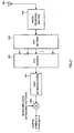
FIG.23 is a block diagram showing the configuration
of a radio communication apparatus according to
Embodiment 5 of the present invention. Parts in FIG.23
identical to those in Embodiment 2 (FIG.10 and FIG.11)
are assigned the same codes as in FIG.10 or FIG.11 and
their detailed explanations are omitted.
The radio communication apparatus shown in FIG.23
is a radio communication apparatus used in an FDD
communication system. A communicating partner radio
communication apparatus that communicates with this
radio communication apparatus also has the same
configuration.
In the radio communication apparatus shown in
FIG.23, the transmitting side comprises, in addition to
the configuration shown in FIG.10, a multiplexer 701,
chip thinning-out section 702, and insertion sections
703-1 through 703-M1, and the receiving side comprises,
in addition to the configuration shown in FIG.11, channel
estimators 704-1 through 704-M1 and a separator 705.
With this configuration, OFDM symbols from a
communicating partner received at the receiving side
undergo FFT processing by the FFT section 203, followed
by input to channel estimators 704-1 through 704-M1 for
each subcarrier component. In channel estimators 704-1
through 704-M1, the channel quality of each subcarrier
is estimated using a pilot signal inserted in each
subcarrier. Pilot signals for performing channel
estimation are pilot signals of fixed power inserted by
insertion sections 703-1 through 703-M1 on the
communicating partner's transmitting side.
Since, with the FDD method, signals are transmitted
and received using different frequency bands on the
transmit channel and receive channel, it is not possible
for an apparatus to ascertain how a signal it has
transmitted has arrived at the communicating partner.
Neither is it possible for the communicating partner to
ascertain how a signal it has transmitted has arrived
at the apparatus. It is therefore necessary for channel
estimation information to be provided by each
communicating partner to the other.
A value (for example, amplitude fluctuation or
phase fluctuation) indicating the channel quality of the
receive channel estimated by channel estimators 704-1
through 704-M1 is input to the multiplexer 701. In the
multiplexer 701, channel estimation information is
multiplexed on digital symbols. By this means, channel
estimation information for a signal received by this
apparatus is transmitted to the communicating partner,
and the communicating partner can be informed the channel
quality of the signal it transmitted (i.e., the
propagation path conditions).
On the receiving side, channel estimation
information for each subcarrier transmitted from a
communicating partner is separated by the separator 705,
and input to the chip thinning-out section 702. In the
chip thinning-out section 702, the chip components of
subcarriers with poor channel quality are thinned out
in accordance with this channel estimation information
for the transmit channel. That is, of the chips output
from frequency domain spreader 301, chip components
assigned to subcarriers whose amplitude fluctuation or
phase fluctuation is equal to or greater than a
predetermined threshold value are thinned out.
Therefore, a signal is not transmitted on a subcarrier
with poor channel quality.
Thus, in this embodiment, OFDM symbols are
generated without assigning a chip component to a
subcarrier with poor channel quality in an FDD
communication system. That is to say, a signal is not
transmitted on a subcarrier with poor channel quality.
By this means, interference with other users can be
reduced when a plurality of users' signals are code
division multiplexed on each subcarrier.
Also, in this embodiment, although transmission
characteristics are somewhat degraded by the
thinning-out of chip components, this can be adequately
compensated for by means of error correcting codes, etc.
(Embodiment 6)
In this embodiment, OFDM symbols are generated
without assigning a chip component to a subcarrier with
poor channel quality in a TDD (Time Division Duplex)
communication system.
FIG.24 is a block diagram showing the configuration
of a radio communication apparatus according to
Embodiment 6 of the present invention. Parts in FIG.24
identical to those in Embodiment 5 (FIG.23) are assigned
the same codes as in FIG.23 and their detailed
explanations are omitted.
The radio communication apparatus shown in FIG.24
is a radio communication apparatus used in a TDD
communication system. A communicating party radio
communication apparatus that communicates with this
radio communication apparatus also has the same
configuration. By means of switching control by a switch
801, antenna 802 and radio transmitting section 105 are
connected at the time of time-slot transmission, and
antenna 802 and radio receiving section 202 are connected
at the time of time-slot reception.
With the TDD method, unlike the FDD method, signals
are transmitted and received using the same frequency
band on the transmit channel and receive channel.
Consequently, if the time slot interval is sufficiently
short and channel conditions scarcely vary in adjacent
transmission and reception times, channel quality
estimated on the receiving side can be used as
transmitting side channel quality.
A value (for example, amplitude fluctuation or
phase fluctuation) indicating the channel quality
estimated by channel estimators 704-1 through 704-M1 is
input to a chip thinning-out section 702 as channel
estimation information. In the chip thinning-out
section 702, the chip components of subcarriers with poor
channel quality are thinned out using this channel
estimation information for the receive channel as
channel estimation information for the transmit channel.
That is, of the chips output from frequency domain
spreader 301, chip components assigned to subcarriers
whose amplitude fluctuation or phase fluctuation is
equal to or greater than a predetermined threshold value
are thinned out. Therefore, a signal is not transmitted
on a subcarrier with poor channel quality.
By this means, the same effect as in Embodiment 5
can be obtained in a TDD communication system. That is
to say, interference with other users can be reduced when
a plurality of users' signals are code division
multiplexed on each subcarrier. Also, as in Embodiment
5, although transmission characteristics are somewhat
degraded by the thinning-out of chip components, this
can be adequately compensated for by means of error
correcting codes, etc.
Embodiments 5 and 6 can also be implemented by being
combined with any one of Embodiments 1 through 4.
Also, in Embodiments 1 through 6, descriptions have
been given taking the OFDM modulation method as an
example of a multicarrier modulation method, but the
present invention can be implemented with any
multicarrier modulation method.
As described above, according to the present
invention it is possible to obtain both a frequency
diversity effect and a path diversity effect in radio
communications in which a multicarrier modulation method
and CDMA method are combined, enabling transmission
characteristics to be improved compared with heretofore.
This application is based on Japanese Patent
Application No.2000-076904 filed on March 17, 2000, and
Japanese Patent Application No.2000-308884 filed on
December 10, 2000, entire content of which is expressly
incorporated by reference herein.
Industrial Applicability
The present invention is applicable to a
communication terminal apparatus and base station
apparatus used in a digital communication system.