EP1179843A2 - Plasma treatment of tantalum nitride compound films formed by chemical vapor deposition - Google Patents
Plasma treatment of tantalum nitride compound films formed by chemical vapor deposition Download PDFInfo
- Publication number
- EP1179843A2 EP1179843A2 EP01306568A EP01306568A EP1179843A2 EP 1179843 A2 EP1179843 A2 EP 1179843A2 EP 01306568 A EP01306568 A EP 01306568A EP 01306568 A EP01306568 A EP 01306568A EP 1179843 A2 EP1179843 A2 EP 1179843A2
- Authority
- EP
- European Patent Office
- Prior art keywords
- tan
- tantalum nitride
- tantalum
- compound layer
- plasma
- Prior art date
- Legal status (The legal status is an assumption and is not a legal conclusion. Google has not performed a legal analysis and makes no representation as to the accuracy of the status listed.)
- Withdrawn
Links
Images


Classifications
-
- H—ELECTRICITY
- H10—SEMICONDUCTOR DEVICES; ELECTRIC SOLID-STATE DEVICES NOT OTHERWISE PROVIDED FOR
- H10W—GENERIC PACKAGES, INTERCONNECTIONS, CONNECTORS OR OTHER CONSTRUCTIONAL DETAILS OF DEVICES COVERED BY CLASS H10
- H10W20/00—Interconnections in chips, wafers or substrates
- H10W20/01—Manufacture or treatment
- H10W20/031—Manufacture or treatment of conductive parts of the interconnections
- H10W20/032—Manufacture or treatment of conductive parts of the interconnections of conductive barrier, adhesion or liner layers
- H10W20/033—Manufacture or treatment of conductive parts of the interconnections of conductive barrier, adhesion or liner layers in openings in dielectrics
- H10W20/035—Manufacture or treatment of conductive parts of the interconnections of conductive barrier, adhesion or liner layers in openings in dielectrics combinations of barrier, adhesion or liner layers, e.g. multi-layered barrier layers
-
- H—ELECTRICITY
- H10—SEMICONDUCTOR DEVICES; ELECTRIC SOLID-STATE DEVICES NOT OTHERWISE PROVIDED FOR
- H10P—GENERIC PROCESSES OR APPARATUS FOR THE MANUFACTURE OR TREATMENT OF DEVICES COVERED BY CLASS H10
- H10P14/00—Formation of materials, e.g. in the shape of layers or pillars
- H10P14/40—Formation of materials, e.g. in the shape of layers or pillars of conductive or resistive materials
- H10P14/418—Formation of materials, e.g. in the shape of layers or pillars of conductive or resistive materials the conductive layers comprising transition metals
-
- H—ELECTRICITY
- H10—SEMICONDUCTOR DEVICES; ELECTRIC SOLID-STATE DEVICES NOT OTHERWISE PROVIDED FOR
- H10W—GENERIC PACKAGES, INTERCONNECTIONS, CONNECTORS OR OTHER CONSTRUCTIONAL DETAILS OF DEVICES COVERED BY CLASS H10
- H10W20/00—Interconnections in chips, wafers or substrates
- H10W20/01—Manufacture or treatment
- H10W20/031—Manufacture or treatment of conductive parts of the interconnections
- H10W20/032—Manufacture or treatment of conductive parts of the interconnections of conductive barrier, adhesion or liner layers
- H10W20/033—Manufacture or treatment of conductive parts of the interconnections of conductive barrier, adhesion or liner layers in openings in dielectrics
-
- H—ELECTRICITY
- H10—SEMICONDUCTOR DEVICES; ELECTRIC SOLID-STATE DEVICES NOT OTHERWISE PROVIDED FOR
- H10W—GENERIC PACKAGES, INTERCONNECTIONS, CONNECTORS OR OTHER CONSTRUCTIONAL DETAILS OF DEVICES COVERED BY CLASS H10
- H10W20/00—Interconnections in chips, wafers or substrates
- H10W20/01—Manufacture or treatment
- H10W20/031—Manufacture or treatment of conductive parts of the interconnections
- H10W20/032—Manufacture or treatment of conductive parts of the interconnections of conductive barrier, adhesion or liner layers
- H10W20/047—Manufacture or treatment of conductive parts of the interconnections of conductive barrier, adhesion or liner layers by introducing additional elements therein
- H10W20/048—Manufacture or treatment of conductive parts of the interconnections of conductive barrier, adhesion or liner layers by introducing additional elements therein by using plasmas or gaseous environments, e.g. by nitriding
-
- H—ELECTRICITY
- H10—SEMICONDUCTOR DEVICES; ELECTRIC SOLID-STATE DEVICES NOT OTHERWISE PROVIDED FOR
- H10W—GENERIC PACKAGES, INTERCONNECTIONS, CONNECTORS OR OTHER CONSTRUCTIONAL DETAILS OF DEVICES COVERED BY CLASS H10
- H10W20/00—Interconnections in chips, wafers or substrates
- H10W20/01—Manufacture or treatment
- H10W20/031—Manufacture or treatment of conductive parts of the interconnections
- H10W20/032—Manufacture or treatment of conductive parts of the interconnections of conductive barrier, adhesion or liner layers
- H10W20/052—Manufacture or treatment of conductive parts of the interconnections of conductive barrier, adhesion or liner layers by treatments not introducing additional elements therein
- H10W20/0523—Manufacture or treatment of conductive parts of the interconnections of conductive barrier, adhesion or liner layers by treatments not introducing additional elements therein by irradiating with ultraviolet or particle radiation
Definitions
- the invention relates to a method of tantalum nitride film deposition and, more particularly, to a method of forming a tantalum nitride compound film having good step-coverage and low resistivity.
- tantalum nitride (TaN) films are often used as barrier layers to inhibit the diffusion of metals into regions underlying the barrier layer. These underlying regions include transistor gates, capacitor dielectric, semiconductor substrates, metal lines, and many other structures that appear in integrated circuits. Tantalum nitride (TaN), for example, is often used as a diffusion barrier for copper (Cu) metallization.
- Cu copper
- TaN layers are typically formed using physical vapor deposition (PVD) and/or chemical vapor deposition (CVD) techniques.
- PVD physical vapor deposition
- CVD chemical vapor deposition
- tantalum may be sputtered from a tantalum target in the presence of a nitrogen source to form TaN films using PVD.
- step coverage of PVD deposited TaN films may become poor.
- the step coverage of a film is a measure of how well such film maintains its nominal thickness as it crosses steps that occur on the surface of a substrate. Step coverage is expressed as the ratio of the minimum thickness of a film as it crosses a step to the nominal thickness of the film on flat regions.
- TaN films may be formed by thermally decomposing a tantalum containing metal-organic precursor or by reacting such tantalum containing metal-organic precursor with a nitrogen source.
- TaN is formed when pentakis(dimethylamido) tantalum (abbreviated PDEAT) (Ta(N(CH 3 ) 2 ) 5 ) decomposes or when pentakis (dimethylamido) tantalum (Ta(N(CH 3 ) 2 ) 5 ) reacts with ammonia (NH 3 ).
- TaN films formed by reacting pentakis(dimethylamido) tantalum (Ta(N(CH 3 ) 2 ) 5 ) with ammonia typically have a low resistivity (e. g., resistivity of about 1,000 ⁇ ohm-cm), but poor step coverage.
- TaN films formed from the decomposition of pentakis(dimethylamido) tantalum (Ta(N(CH 3 ) 2 ) 5 ) typically have good step coverage, but high resistivity (e. g., resistivity of about 100,000 ⁇ ohm-cm).
- a method of forming tantalum nitride (TaN) compound layers for use in integrated circuit fabrication processes is provided.
- the tantalum nitride (TaN) compound layer is formed by thermally decomposing a tantalum containing metal organic precursor. After the tantalum nitride (TaN) compound layer is formed, it is plasma treated.
- the tantalum nitride (TaN) compound layer is preferably plasma treated with an argon (Ar) based plasma.
- the tantalum nitride (TaN) compound layer is compatible with integrated circuit fabrication processes.
- the tantalum nitride (TaN) compound layer is used as a barrier layer for fabricating integrated circuit structures such as, for example, vias.
- a preferred process sequence includes providing a substrate having a dielectric material thereon.
- the dielectric material has vias therein.
- a tantalum nitride (TaN) compound layer is formed on the dielectric material by thermally decomposing a tantalum containing metal organic precursor.
- the tantalum nitride (TaN) compound layer is formed on the dielectric material, it is plasma treated, preferably with an argon (Ar) based plasma.
- the integrated circuit structure is completed by filling the vias with a conductive material.
- FIG. 1 is a schematic representation of a wafer processing system 10 that can be used to perform tantalum nitride (TaN) compound film formation in accordance with embodiments described herein.
- System 10 typically comprises a process chamber 100, a gas panel 130, a control unit 110, along with other hardware components such as power supplies 106 and vacuum pumps 102.
- process chamber 100 has been previously described in commonly assigned U. S. Patent application Serial No. 09/211,998, entitled “High Temperature Chemical Vapor Deposition Chamber", filed December 14, 1998, and is herein incorporated by reference. The salient features of this system 10 are briefly described below.
- the process chamber 100 generally houses a support pedestal 150, which is used to support a substrate such as a semiconductor wafer 190.
- This pedestal 150 can typically be moved in a vertical direction inside the chamber 100 using a displacement mechanism (not shown).
- the wafer 190 can be heated to some desired temperature prior to the tantalum nitride (TaN) compound film deposition.
- the wafer support pedestal 150 is heated by an embedded heater element 170.
- the pedestal 150 may be resistively heated by applying an electric current from an AC power supply 106 to the heater element 170.
- the wafer 190 is, in turn, heated by the pedestal 150.
- a temperature sensor 172 such as a thermocouple, is also embedded in the wafer support pedestal 150 to monitor the temperature of the pedestal 150 in a conventional manner. The measured temperature is used in a feedback loop to control the power supplied to the heater element 170, such that the wafer temperature can be maintained or controlled at a desired temperature which is suitable for the particular process application.
- the pedestal is optionally heated using radiant heat (not shown).
- a vacuum pump 102 is used to evacuate the process chamber 100 and to maintain the proper gas flows and pressure inside the chamber 100.
- a showerhead 120 through which process gases are introduced into the chamber 100, is located above the wafer support pedestal 150.
- the showerhead 120 is coupled to a gas panel 130, which controls and supplies various gases used in different steps of the process sequence.
- the showerhead 120 and the wafer support pedestal 150 also form a pair of spaced apart electrodes. When an electric field is generated between these electrodes, the process gases introduced into the chamber 100 are ignited into a plasma. Typically, the electric field is generated by connecting the wafer support pedestal 150 to a source of radio frequency (RF) power (not shown) through a matching network (not shown). Alternatively, the RF power source and matching network may be coupled to the showerhead 120, or coupled to both the showerhead 120 and the wafer support pedestal 150.
- RF radio frequency
- Plasma enhanced chemical vapor deposition (PECVD) techniques promote excitation and/or disassociation of the reactant gases by the application of the electric field to the reaction zone near the substrate surface, creating a plasma of reactive species.
- the reactivity of the species in the plasma reduces the energy required for a chemical reaction to take place, in effect lowering the required temperature for such PECVD processes.
- the showerhead 120 allows process gases from the gas panel 130 to be uniformly introduced and distributed in the process chamber 100.
- control unit 110 comprises a central processing unit (CPU) 113, support circuitry 114, and memories containing associated control software 116.
- the control unit 110 is responsible for automated control of the numerous steps required for wafer processing - such as wafer transport, gas flow control, RF power control, temperature control, chamber evacuation, and other steps.
- Bi-directional communications between the control unit 110 and the various components of the wafer processing system 10 are handled through numerous signal cables collectively referred to as signal buses 118, some of which are illustrated in FIG. 1.
- the central processing unit (CPU) 113 may be one of any form of general purpose computer processor that can be used in an industrial setting for controlling process chambers as well as sub-processors.
- the computer may use any suitable memory, such as random access memory, read only memory, floppy disk drive, hard drive, or any other form of digital storage, local or remote.
- Various support circuits may be coupled to the CPU for supporting the processor in a conventional manner. Process sequence routines as required may be stored in the memory or executed by a second CPU that is remotely located.
- the process sequence routines are executed after the substrate 190 is positioned on the wafer support pedestal 150.
- the process sequence routines when executed, transform the general purpose computer into a specific process computer that controls the chamber operation so that the deposition process is performed.
- the chamber operation may be controlled using remotely located hardware, as an application specific integrated circuit or other type of hardware implementation, or a combination of software or hardware.
- a remote plasma source 150 may be coupled to wafer processing system 10, as shown in FIG. 2, to provide a remotely generated plasma to the process chamber 100.
- the remote plasma source 150 includes a gas supply 153, a gas flow controller 155, a plasma chamber 151, and a chamber inlet 157.
- the gas flow controller 155 controls the flow of process gas from the gas supply 153 to the plasma chamber 151.
- a remote plasma may be generated by applying an electric field to the process gas in the plasma chamber 151, creating a plasma of reactive species.
- the electric field is generated in the plasma chamber 151 using a RF power source (not shown).
- the reactive species generated in the remote plasma source 150 are introduced into the process chamber 100 through inlet 157.
- Tantalum Nitride (TaN) Compound Layer Integration
- the following embodiment is a method for tantalum nitride (TaN) compound layer integration, which advantageously provides tantalum nitride (TaN) compound layers with good step coverage and a low resistivity.
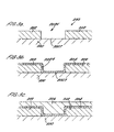
- FIGS. 3a-3c illustrate an integrated circuit structure at different stages of a fabrication sequence, incorporating a tantalum nitride (TaN) compound barrier layer.
- the substrate 200 refers to any workpiece upon which film processing is performed, and a substrate structure 250 is used to generally denote the substrate 200 as well as other material layers formed on the substrate 200.
- the substrate 200 may be a silicon semiconductor wafer, or other material layer, which has been formed on the wafer.
- FIG. 3a shows a cross-sectional view of a substrate structure 250, having a material layer 202 thereon.
- the material layer 202 may be an oxide (e. g., silicon dioxide, fluorosilicate glass (FSG), undoped silicate glass (USG)).
- the material layer 202 has been conventionally formed and patterned to provide a contact hole 202H having sidewalls 202S, and extending to the top surface 200T of the substrate 200.
- FIG. 3b depicts a tantalum nitride (TaN) compound layer 204 formed on the substrate structure 250 of FIG. 3a.
- the tantalum nitride (TaN) compound layer 204 is formed by thermally decomposing a tantalum containing metal organic precursor.
- the tantalum containing metal organic precursor may be selected, for example, from the group of pentakis(diethylamido) tantalum (PDEAT) (Ta(NEt 2 ) 5 ), pentakis(ethylmethylamido) tantalum (PEMAT) (Ta(N(Et)(Me)) 5 ), pentakis(dimethylamido) tantalum (PDMAT) (Ta(NMe 2 ) 5 ), tetrakis(ethylmethylamido) tantalum (TEMAT) (Ta(N(Et)(Me)) 4 ), tetrakis(diethylamido) tantalum (TDEAT) (Ta(NEt 2 ) 4 ), tetrakis(dimethylamido) tantalum (TDMAT) (Ta(NMe 2 ) 4 ), among others.
- PDEAT pentakis(diethylamido) tantalum
- PEMAT pen
- Carrier gases such as hydrogen (H 2 ), helium (He), argon (Ar), nitrogen (N 2 ), among others may be mixed with the tantalum containing metal organic precursor.
- the following deposition process parameters can be used to form the tantalum nitride (TaN) compound layer in a deposition chamber similar to that shown in FIG. 1.
- the process parameters range from a wafer temperature of about 200 °C to about 600 °C, a chamber pressure of about 0.1 torr to about 100 torr, a tantalum containing metal organic precursor flow rate of about 0.1 sccm to about 1000 sccm, and a carrier gas flow rate of about 10 sccm to about 10,000 sccm.
- the above process parameters provide a deposition rate for the tantalum nitride (TaN) compound layer in a range of about 0.1 ⁇ /min to about 1,000 ⁇ /min when implemented on a 200 mm (millimeter) substrate in a deposition chamber available from Applied Materials, Inc., located in Santa Clara, California.
- deposition chambers are within the scope of the invention, and the parameters listed above may vary according to the particular deposition chamber used to form the tantalum nitride (TaN) compound layer.
- other deposition chambers may have a larger (e. g., configured to accommodate 300 mm substrates) or smaller volume, requiring gas flow rates that are larger or smaller than those recited for deposition chambers available from Applied Materials, Inc.
- tantalum nitride (TaN) compound layers that contain carbon (C).
- a typical composition for the tantalum nitride (TaN) compound layers includes tantalum (Ta), nitrogen (N), carbon (C), and oxygen (O) in a ratio of about 4Ta : 2.5N : 3C : 0.50.
- the tantalum nitride (TaN) compound layers may include a mixture of both tantalum nitride (TaN) and tantalum carbide (TaC).
- the thickness of the tantalum nitride (TaN) compound layer 204 is variable depending on the specific stage of processing. Typically, the tantalum nitride (TaN) compound layer 204 is deposited to a thickness of about 50 ⁇ to about 100 ⁇ .
- the tantalum nitride (TaN) compound layer 204 is plasma treated.
- the tantalum nitride (TaN) compound layer 204 is preferably plasma treated with an argon (Ar) based plasma.
- Carrier gases such as hydrogen (H 2 ), nitrogen (N 2 ), helium (He), among others may be mixed with the argon.
- a hydrogen (H 2 ) based plasma, or a helium (He) based plasma may be used to plasma treat the tantalum nitride (TaN) compound layer 204.
- the following process parameters can be used to plasma treat the tantalum nitride (TaN) compound layer 204 in a process chamber similar to that shown in FIGS. 1 or 2.
- the process parameters range from a wafer temperature of about 200 °C to about 600 °C, a chamber pressure of about 0.1 torr to about 100 torr, an argon gas flow rate of about 10 sccm to about 10,000 sccm, and a radio frequency (RF) power of about 50 watts to about 2,000 watts.
- the tantalum nitride (TaN) compound layer 204 is plasma treated for less than about 300 seconds.
- tantalum nitride (TaN) compound layer 204 The plasma treatment of the tantalum nitride (TaN) compound layer 204 is believed to densify such compound layer so as to reduce the resistivity thereof.
- the plasma treatment of the tantalum nitride (TaN) compound layer 204 is optionally performed as a multi-step process, wherein the plasma treatment is followed by a chemical treatment step.
- a chemical treatment step For example, an argon-based (Ar) plasma may be used to treat the tantalum nitride (TaN) compound layer 204, followed by chemical treatment using, for example, silane (SiH 4 ).
- the plasma treatment of the tantalum nitride (TaN) compound layer has directionality.
- an argon-based plasma is believed to be effective for lowering the resistivity of tantalum nitride (TaN) compound surfaces that are parallel to the wafer surface (e. g., surfaces 202T of hole 202H).
- the resistivity of the tantalum nitride (TaN) compound layer 204 also increased.
- Chemical treatment of the tantalum nitride (TaN) compound layer 204 using, for example, silane (SiH 4 ) gas is believed to reduce the resistivity of surfaces that are perpendicular to the wafer surface (e. g., surfaces 202S of hole 202H).
- Additional tantalum nitride (TaN) compound layers may optionally be deposited one over another so as to form tantalum nitride (TaN) compound layers having thicknesses in a range of about 30 ⁇ to about 5,000 ⁇ . After each tantalum nitride (TaN) compound layer is formed it is plasma treated to reduce the resistivity thereof.
- the holes 202H are filled with a conductive material 206 such as, for example, aluminum (Al), copper (Cu), tungsten (W), and combinations thereof, among others.
- a conductive material 206 such as, for example, aluminum (Al), copper (Cu), tungsten (W), and combinations thereof, among others.
- the conductive material 206 may be deposited using chemical vapor deposition (CVD), physical vapor deposition (PVD), electroplating, or combinations thereof.
Landscapes
- Chemical Vapour Deposition (AREA)
- Internal Circuitry In Semiconductor Integrated Circuit Devices (AREA)
- Electrodes Of Semiconductors (AREA)
Abstract
Description
Claims (31)
- A method of thin film deposition for integrated circuit fabrication, comprising the steps of:(a) forming a tantalum nitride (TaN) compound layer on a substrate;(b) plasma treating the tantalum nitride (TaN) compound layer.
- The method of claim 1, wherein step (a) comprises:positioning the substrate in a deposition chamber;providing a gas mixture to the deposition chamber wherein the gas mixture comprises a tantalum (Ta) containing metal organic precursor; andthermally decomposing the Ta containing metal organic precursor to form a tantalum nitride (TaN) compound layer on the substrate.
- The method of claim 1 or claim 2, wherein the plasma of step (b) is generated by:providing a gas mixture to a process chamber; andapplying an electric field to the gas mixture in the process chamber to generate the plasma.
- The method of any one of claims 1 to 3, wherein step (b) comprises:(c) plasma treating the tantalum (TaN) compound layer using an argon (Ar) based plasma; and(d) treating the tantalum nitride (TaN) compound layer in a silane (SiH4) based atmosphere.
- A method of forming a device, comprising:(a) providing a substrate having a dielectric layer thereon, wherein the dielectric layer has vias therein;(b) forming a tantalum nitride (TaN) compound layer on the dielectric layer;(c) plasma treating the tantalum nitride (TaN) compound layer; and(d) filling the vias with a conductive material.
- The method of claim 5, wherein the conductive material filling the vias has a resistivity less than about 10 µΩ-cm (micro-ohms-centimeters).
- The method of claim 5 or claim 6, wherein the dielectric layer is selected from silicon dioxide, fluorosilicate glass (FSG), undoped silicate glass (USG), and combinations thereof.
- The method of any one of claims 5 to 7, wherein the conductive material filling the vias is selected from copper (Cu), aluminum (Al), tungsten (W), and combinations thereof.
- The method of any one of claims 5 to 8, wherein step (b) comprises:positioning the substrate in a deposition chamber;providing a gas mixture to the deposition chamber wherein the gas mixture comprises a tantalum (Ta) containing metal organic precursor; andthermally decomposing the Ta containing metal organic precursor to form a tantalum nitride (TaN) compound layer on the substrate.
- The method of any one of claims 2 to 9, wherein the gas mixture further comprises a carrier gas.
- The method of claim 10, wherein the carrier gas is selected from hydrogen (H2), argon (Ar), helium (He), nitrogen (N2), and combinations of two or more thereof.
- The method of claim 10 or claim 11, wherein the carrier gas is provided to the deposition chamber at a flow rate in the range of from about 10 sccm to about 10,000 sccm.
- The method of any one of claims 2 to 12, wherein the Ta containing metal organic precursor is selected from pentakis(diethylamido) tantalum (PDEAT) (Ta(NEt2)5), pentakis (ethylmethylamido) tantalum (PEMAT) (Ta(N(Et)(Me))5), pentakis(dimethylamido) tantalum (PDMAT) (Ta(NMe2)5), tetrakis (ethylmethylamido) tantalum (TEMAT) (Ta(N(Et)(Me))4), tetrakis (diethylamido) tantalum (TDEAT) (Ta(NEt2)4), tetrakis(dimethylamido) tantalum (TDMAT) (Ta(NMe2)4), among others, and combinations of two or more thereof.
- The method of any one of claims 1 to 13, wherein the substrate is heated to a temperature of between about 200 °C to about 600 °C.
- The method of any one of claims 2 to 14, wherein the deposition chamber is maintained at a pressure between about 0.1 torr to about 100 torr.
- The method of any one of claims 2 to 15, wherein the tantalum containing metal organic precursor is provided to the deposition chamber at a flow rate in the range of from about 0.1 sccm to about 1,000 sccm.
- The method of any one of claims 5 to 16, wherein the plasma of step (c) is generated by:providing a gas mixture to a process chamber; andapplying an electric field to the gas mixture in the process chamber to generate the plasma.
- The method of claim 3 or claim 17, wherein the gas mixture comprises one or more gases selected from molecular hydrogen (H2), argon (Ar), helium (He), nitrogen (N2), among others.
- The method of any one of claims 3, 17 and 18, wherein the process chamber is maintained at a pressure in the range of from about 0.1 torr to about 100 torr.
- The method of any one of claims 3, 17 to 19, wherein the gas mixture is provided to the deposition chamber at a flow rate in the range of from about 10 sccm to about 10,000 sccm.
- The method of any one of claims 3, 17 to 20, wherein the electric field is a radio frequency (RF) power.
- The method of claim 21, wherein the RF power is in the range of from about 50 watts to about 2,000 watts.
- The method of any one of claims 3, 17 to 22, wherein the plasma is generated in a process chamber used for tantalum nitride (TaN) compound layer deposition.
- The method of any one of claims 3, 17 to 22, wherein the plasma is generated in a process chamber that is coupled to a process chamber used for tantalum nitride (TaN) compound layer deposition.
- The method of any one of claims 5 to 16, wherein step (c) comprises:(e) plasma treating the tantalum nitride (TaN) compound layer using an argon (Ar) based plasma; and(f) treating the tantalum nitride (TaN) compound layer in a silane (SiH4) based atmosphere.
- A computer storage medium containing a software routine that, when executed, causes a general purpose computer to control a deposition chamber using a layer deposition method, comprising:(a) forming a tantalum nitride (TaN) compound layer on a substrate;(b) plasma treating the tantalum nitride (TaN) compound layer.
- A computer storage medium as claimed in claim 26, wherein said method includes step(s) as defined in any one of claims 1 to 4, 10 to 16, and 18 to 24.
- A computer storage medium containing a software routine that, when executed, causes a general purpose computer to control a deposition chamber using a method of forming a device, comprising:(a) providing a substrate having a dielectric layer thereon, wherein the dielectric layer has vias therein;(b) forming a tantalum nitride (TaN) compound layer on the dielectric layer;(c) plasma treating the tantalum nitride (TaN) compound layer; and(d) filling the vias with a conductive material.
- A computer storage medium as claimed in claim 28, wherein said method includes step(s) as defined in any one of claims 5 to 25.
- A computer program product, which when read by a computer causes the said computer to control an apparatus using a method comprising the step(s) as defined in any one of claims 1 to 25.
- A storage medium upon which is stored a computer program product as defined in claim 30.
Applications Claiming Priority (2)
| Application Number | Priority Date | Filing Date | Title |
|---|---|---|---|
| US629778 | 2000-07-31 | ||
| US09/629,778 US6455421B1 (en) | 2000-07-31 | 2000-07-31 | Plasma treatment of tantalum nitride compound films formed by chemical vapor deposition |
Publications (2)
| Publication Number | Publication Date |
|---|---|
| EP1179843A2 true EP1179843A2 (en) | 2002-02-13 |
| EP1179843A3 EP1179843A3 (en) | 2003-04-09 |
Family
ID=24524445
Family Applications (1)
| Application Number | Title | Priority Date | Filing Date |
|---|---|---|---|
| EP01306568A Withdrawn EP1179843A3 (en) | 2000-07-31 | 2001-07-31 | Plasma treatment of tantalum nitride compound films formed by chemical vapor deposition |
Country Status (5)
| Country | Link |
|---|---|
| US (2) | US6455421B1 (en) |
| EP (1) | EP1179843A3 (en) |
| JP (1) | JP2002151437A (en) |
| KR (1) | KR20020011126A (en) |
| TW (1) | TW510014B (en) |
Families Citing this family (23)
| Publication number | Priority date | Publication date | Assignee | Title |
|---|---|---|---|---|
| US6951804B2 (en) | 2001-02-02 | 2005-10-04 | Applied Materials, Inc. | Formation of a tantalum-nitride layer |
| US6777327B2 (en) * | 2001-03-28 | 2004-08-17 | Sharp Laboratories Of America, Inc. | Method of barrier metal surface treatment prior to Cu deposition to improve adhesion and trench filling characteristics |
| US7005392B2 (en) * | 2001-03-30 | 2006-02-28 | Advanced Technology Materials, Inc. | Source reagent compositions for CVD formation of gate dielectric thin films using amide precursors and method of using same |
| US6849545B2 (en) * | 2001-06-20 | 2005-02-01 | Applied Materials, Inc. | System and method to form a composite film stack utilizing sequential deposition techniques |
| US7098131B2 (en) * | 2001-07-19 | 2006-08-29 | Samsung Electronics Co., Ltd. | Methods for forming atomic layers and thin films including tantalum nitride and devices including the same |
| US7105444B2 (en) * | 2001-07-19 | 2006-09-12 | Samsung Electronics Co., Ltd. | Method for forming a wiring of a semiconductor device, method for forming a metal layer of a semiconductor device and apparatus for performing the same |
| US6607976B2 (en) * | 2001-09-25 | 2003-08-19 | Applied Materials, Inc. | Copper interconnect barrier layer structure and formation method |
| KR100505043B1 (en) * | 2002-05-25 | 2005-07-29 | 삼성전자주식회사 | Method for forming a capacitor |
| US7067422B2 (en) * | 2004-03-31 | 2006-06-27 | Tokyo Electron Limited | Method of forming a tantalum-containing gate electrode structure |
| KR100639458B1 (en) * | 2004-12-30 | 2006-10-26 | 동부일렉트로닉스 주식회사 | Diffusion preventing film forming method using TASI film and metal wiring forming method using same |
| JP4931171B2 (en) * | 2005-03-03 | 2012-05-16 | 株式会社アルバック | Method for forming tantalum nitride film |
| US20070048962A1 (en) * | 2005-08-26 | 2007-03-01 | Texas Instruments Incorporated | TaN integrated circuit (IC) capacitor formation |
| US20070119370A1 (en) | 2005-11-04 | 2007-05-31 | Paul Ma | Apparatus and process for plasma-enhanced atomic layer deposition |
| US7959985B2 (en) * | 2006-03-20 | 2011-06-14 | Tokyo Electron Limited | Method of integrating PEALD Ta-containing films into Cu metallization |
| US7407876B2 (en) * | 2006-03-20 | 2008-08-05 | Tokyo Electron Limited | Method of plasma enhanced atomic layer deposition of TaC and TaCN films having good adhesion to copper |
| US7750173B2 (en) | 2007-01-18 | 2010-07-06 | Advanced Technology Materials, Inc. | Tantalum amido-complexes with chelate ligands useful for CVD and ALD of TaN and Ta205 thin films |
| EP2151091A4 (en) * | 2007-05-17 | 2010-07-21 | Fat Free Mobile Inc | METHOD AND SYSTEM FOR TRANSCODING WEB PAGES BY SELECTION LIMITATION THROUGH DIRECTIONAL REFERENCES |
| US8026168B2 (en) * | 2007-08-15 | 2011-09-27 | Tokyo Electron Limited | Semiconductor device containing an aluminum tantalum carbonitride barrier film and method of forming |
| US20090246952A1 (en) * | 2008-03-28 | 2009-10-01 | Tokyo Electron Limited | Method of forming a cobalt metal nitride barrier film |
| US7985680B2 (en) * | 2008-08-25 | 2011-07-26 | Tokyo Electron Limited | Method of forming aluminum-doped metal carbonitride gate electrodes |
| US8513107B2 (en) * | 2010-01-26 | 2013-08-20 | Taiwan Semiconductor Manufacturing Co., Ltd. | Replacement gate FinFET devices and methods for forming the same |
| JP5683388B2 (en) | 2010-08-19 | 2015-03-11 | 株式会社日立国際電気 | Semiconductor device manufacturing method, substrate processing method, and substrate processing apparatus |
| FR3099490B1 (en) | 2019-08-02 | 2022-12-02 | X Fab France | Method of forming a low resistivity tantalum film |
Family Cites Families (21)
| Publication number | Priority date | Publication date | Assignee | Title |
|---|---|---|---|---|
| EP0285614A1 (en) * | 1986-10-06 | 1988-10-12 | Stéfan Grigore DE FAY | Method and portable device for acquiring, storing and optionally processing and reproducing graphic signs from any medium |
| US5989999A (en) | 1994-11-14 | 1999-11-23 | Applied Materials, Inc. | Construction of a tantalum nitride film on a semiconductor wafer |
| US5852676A (en) * | 1995-04-11 | 1998-12-22 | Teraform Inc. | Method and apparatus for locating and identifying fields within a document |
| US5685960A (en) * | 1995-11-27 | 1997-11-11 | Applied Materials, Inc. | Method for forming aluminum contacts |
| US5668054A (en) | 1996-01-11 | 1997-09-16 | United Microelectronics Corporation | Process for fabricating tantalum nitride diffusion barrier for copper matallization |
| US5989652A (en) * | 1997-01-31 | 1999-11-23 | Tokyo Electron Limited | Method of low temperature plasma enhanced chemical vapor deposition of tin film over titanium for use in via level applications |
| US6208435B1 (en) * | 1997-03-25 | 2001-03-27 | Jan Scott Zwolinski | Method and apparatus for providing a handheld scanner-dictionary apparatus |
| US6153519A (en) * | 1997-03-31 | 2000-11-28 | Motorola, Inc. | Method of forming a barrier layer |
| US6015917A (en) | 1998-01-23 | 2000-01-18 | Advanced Technology Materials, Inc. | Tantalum amide precursors for deposition of tantalum nitride on a substrate |
| US6297147B1 (en) * | 1998-06-05 | 2001-10-02 | Applied Materials, Inc. | Plasma treatment for ex-situ contact fill |
| US6307955B1 (en) * | 1998-12-18 | 2001-10-23 | Topaz Systems, Inc. | Electronic signature management system |
| US6204204B1 (en) * | 1999-04-01 | 2001-03-20 | Cvc Products, Inc. | Method and apparatus for depositing tantalum-based thin films with organmetallic precursor |
| US6054398A (en) * | 1999-05-14 | 2000-04-25 | Advanced Micro Devices, Inc. | Semiconductor interconnect barrier for fluorinated dielectrics |
| US6543052B1 (en) * | 1999-07-09 | 2003-04-01 | Fujitsu Limited | Internet shopping system utilizing set top box and voice recognition |
| US6546385B1 (en) * | 1999-08-13 | 2003-04-08 | International Business Machines Corporation | Method and apparatus for indexing and searching content in hardcopy documents |
| US6297491B1 (en) * | 1999-08-30 | 2001-10-02 | Gateway, Inc. | Media scanner |
| AU2001229421A1 (en) * | 2000-01-13 | 2001-07-24 | Orbidex, Inc. | System and method of searching and gathering information on-line and off-line |
| US6704024B2 (en) * | 2000-08-07 | 2004-03-09 | Zframe, Inc. | Visual content browsing using rasterized representations |
| US20020135815A1 (en) * | 2001-01-22 | 2002-09-26 | Time Domain Corporation | Hand-held scanner with impulse radio wireless interface |
| JP4245883B2 (en) * | 2002-09-13 | 2009-04-02 | 株式会社日立製作所 | Authenticity management method and system for electronic document and print medium thereof, program, and recording medium |
| JP2004348591A (en) * | 2003-05-23 | 2004-12-09 | Canon Inc | Document search method and apparatus |
-
2000
- 2000-07-31 US US09/629,778 patent/US6455421B1/en not_active Expired - Fee Related
-
2001
- 2001-07-27 TW TW090118498A patent/TW510014B/en not_active IP Right Cessation
- 2001-07-31 KR KR1020010046368A patent/KR20020011126A/en not_active Withdrawn
- 2001-07-31 JP JP2001266506A patent/JP2002151437A/en not_active Withdrawn
- 2001-07-31 EP EP01306568A patent/EP1179843A3/en not_active Withdrawn
-
2002
- 2002-07-30 US US10/208,461 patent/US20020192952A1/en not_active Abandoned
Also Published As
| Publication number | Publication date |
|---|---|
| EP1179843A3 (en) | 2003-04-09 |
| US20020192952A1 (en) | 2002-12-19 |
| JP2002151437A (en) | 2002-05-24 |
| TW510014B (en) | 2002-11-11 |
| KR20020011126A (en) | 2002-02-07 |
| US6455421B1 (en) | 2002-09-24 |
Similar Documents
| Publication | Publication Date | Title |
|---|---|---|
| US6455421B1 (en) | Plasma treatment of tantalum nitride compound films formed by chemical vapor deposition | |
| US20020114886A1 (en) | Method of tisin deposition using a chemical vapor deposition process | |
| US11587829B2 (en) | Doping control of metal nitride films | |
| US7772121B2 (en) | Method of forming a trench structure | |
| US6218301B1 (en) | Deposition of tungsten films from W(CO)6 | |
| US7838441B2 (en) | Deposition and densification process for titanium nitride barrier layers | |
| US6933021B2 (en) | Method of TiSiN deposition using a chemical vapor deposition (CVD) process | |
| JP4947840B2 (en) | Metal nitride / metal stack processing | |
| US20030072884A1 (en) | Method of titanium and titanium nitride layer deposition | |
| US20110306203A1 (en) | Interconnect structure and method of manufacturing a damascene structure | |
| TWI821661B (en) | Doping of metal barrier layers | |
| JP2001291682A (en) | Plasma treatment of titanium nitride film formed by chemical vapor deposition | |
| US20020132473A1 (en) | Integrated barrier layer structure for copper contact level metallization | |
| JP2003528215A (en) | Improved PECVD and CVD method for WNx deposition | |
| WO2002021593A9 (en) | Method of forming titanium nitride (tin) films using metal-organic chemical vapor deposition (mocvd) | |
| US7189649B2 (en) | Method of forming a material film |
Legal Events
| Date | Code | Title | Description |
|---|---|---|---|
| PUAI | Public reference made under article 153(3) epc to a published international application that has entered the european phase |
Free format text: ORIGINAL CODE: 0009012 |
|
| AK | Designated contracting states |
Kind code of ref document: A2 Designated state(s): AT BE CH CY DE DK ES FI FR GB GR IE IT LI LU MC NL PT SE TR |
|
| AX | Request for extension of the european patent |
Free format text: AL;LT;LV;MK;RO;SI |
|
| PUAL | Search report despatched |
Free format text: ORIGINAL CODE: 0009013 |
|
| AK | Designated contracting states |
Kind code of ref document: A3 Designated state(s): AT BE CH CY DE DK ES FI FR GB GR IE IT LI LU MC NL PT SE TR Designated state(s): AT BE CH CY DE DK ES FI FR GB GR IE IT LI LU MC NL PT SE TR |
|
| AX | Request for extension of the european patent |
Extension state: AL LT LV MK RO SI |
|
| AKX | Designation fees paid | ||
| REG | Reference to a national code |
Ref country code: DE Ref legal event code: 8566 |
|
| STAA | Information on the status of an ep patent application or granted ep patent |
Free format text: STATUS: THE APPLICATION IS DEEMED TO BE WITHDRAWN |
|
| 18D | Application deemed to be withdrawn |
Effective date: 20031010 |