EP1178535A2 - Photodetector array and optical communication monitoring - Google Patents
Photodetector array and optical communication monitoring Download PDFInfo
- Publication number
- EP1178535A2 EP1178535A2 EP01117793A EP01117793A EP1178535A2 EP 1178535 A2 EP1178535 A2 EP 1178535A2 EP 01117793 A EP01117793 A EP 01117793A EP 01117793 A EP01117793 A EP 01117793A EP 1178535 A2 EP1178535 A2 EP 1178535A2
- Authority
- EP
- European Patent Office
- Prior art keywords
- photodetectors
- photodetector array
- photodetector
- pitch
- wavelength
- Prior art date
- Legal status (The legal status is an assumption and is not a legal conclusion. Google has not performed a legal analysis and makes no representation as to the accuracy of the status listed.)
- Withdrawn
Links
Images

Classifications
-
- G—PHYSICS
- G01—MEASURING; TESTING
- G01J—MEASUREMENT OF INTENSITY, VELOCITY, SPECTRAL CONTENT, POLARISATION, PHASE OR PULSE CHARACTERISTICS OF INFRARED, VISIBLE OR ULTRAVIOLET LIGHT; COLORIMETRY; RADIATION PYROMETRY
- G01J3/00—Spectrometry; Spectrophotometry; Monochromators; Measuring colours
- G01J3/12—Generating the spectrum; Monochromators
- G01J3/18—Generating the spectrum; Monochromators using diffraction elements, e.g. grating
-
- G—PHYSICS
- G01—MEASURING; TESTING
- G01J—MEASUREMENT OF INTENSITY, VELOCITY, SPECTRAL CONTENT, POLARISATION, PHASE OR PULSE CHARACTERISTICS OF INFRARED, VISIBLE OR ULTRAVIOLET LIGHT; COLORIMETRY; RADIATION PYROMETRY
- G01J3/00—Spectrometry; Spectrophotometry; Monochromators; Measuring colours
- G01J3/02—Details
- G01J3/0256—Compact construction
-
- G—PHYSICS
- G01—MEASURING; TESTING
- G01J—MEASUREMENT OF INTENSITY, VELOCITY, SPECTRAL CONTENT, POLARISATION, PHASE OR PULSE CHARACTERISTICS OF INFRARED, VISIBLE OR ULTRAVIOLET LIGHT; COLORIMETRY; RADIATION PYROMETRY
- G01J3/00—Spectrometry; Spectrophotometry; Monochromators; Measuring colours
- G01J3/28—Investigating the spectrum
- G01J3/2803—Investigating the spectrum using photoelectric array detector
-
- G—PHYSICS
- G02—OPTICS
- G02B—OPTICAL ELEMENTS, SYSTEMS OR APPARATUS
- G02B6/00—Light guides; Structural details of arrangements comprising light guides and other optical elements, e.g. couplings
- G02B6/24—Coupling light guides
- G02B6/26—Optical coupling means
- G02B6/28—Optical coupling means having data bus means, i.e. plural waveguides interconnected and providing an inherently bidirectional system by mixing and splitting signals
- G02B6/293—Optical coupling means having data bus means, i.e. plural waveguides interconnected and providing an inherently bidirectional system by mixing and splitting signals with wavelength selective means
- G02B6/29304—Optical coupling means having data bus means, i.e. plural waveguides interconnected and providing an inherently bidirectional system by mixing and splitting signals with wavelength selective means operating by diffraction, e.g. grating
- G02B6/29305—Optical coupling means having data bus means, i.e. plural waveguides interconnected and providing an inherently bidirectional system by mixing and splitting signals with wavelength selective means operating by diffraction, e.g. grating as bulk element, i.e. free space arrangement external to a light guide
- G02B6/2931—Diffractive element operating in reflection
-
- G—PHYSICS
- G02—OPTICS
- G02B—OPTICAL ELEMENTS, SYSTEMS OR APPARATUS
- G02B6/00—Light guides; Structural details of arrangements comprising light guides and other optical elements, e.g. couplings
- G02B6/24—Coupling light guides
- G02B6/26—Optical coupling means
- G02B6/28—Optical coupling means having data bus means, i.e. plural waveguides interconnected and providing an inherently bidirectional system by mixing and splitting signals
- G02B6/293—Optical coupling means having data bus means, i.e. plural waveguides interconnected and providing an inherently bidirectional system by mixing and splitting signals with wavelength selective means
- G02B6/29379—Optical coupling means having data bus means, i.e. plural waveguides interconnected and providing an inherently bidirectional system by mixing and splitting signals with wavelength selective means characterised by the function or use of the complete device
- G02B6/2938—Optical coupling means having data bus means, i.e. plural waveguides interconnected and providing an inherently bidirectional system by mixing and splitting signals with wavelength selective means characterised by the function or use of the complete device for multiplexing or demultiplexing, i.e. combining or separating wavelengths, e.g. 1xN, NxM
- G02B6/29382—Optical coupling means having data bus means, i.e. plural waveguides interconnected and providing an inherently bidirectional system by mixing and splitting signals with wavelength selective means characterised by the function or use of the complete device for multiplexing or demultiplexing, i.e. combining or separating wavelengths, e.g. 1xN, NxM including at least adding or dropping a signal, i.e. passing the majority of signals
- G02B6/29385—Channel monitoring, e.g. by tapping
-
- G—PHYSICS
- G02—OPTICS
- G02B—OPTICAL ELEMENTS, SYSTEMS OR APPARATUS
- G02B6/00—Light guides; Structural details of arrangements comprising light guides and other optical elements, e.g. couplings
- G02B6/24—Coupling light guides
- G02B6/42—Coupling light guides with opto-electronic elements
- G02B6/4201—Packages, e.g. shape, construction, internal or external details
- G02B6/4204—Packages, e.g. shape, construction, internal or external details the coupling comprising intermediate optical elements, e.g. lenses, holograms
- G02B6/4215—Packages, e.g. shape, construction, internal or external details the coupling comprising intermediate optical elements, e.g. lenses, holograms the intermediate optical elements being wavelength selective optical elements, e.g. variable wavelength optical modules or wavelength lockers
-
- H—ELECTRICITY
- H10—SEMICONDUCTOR DEVICES; ELECTRIC SOLID-STATE DEVICES NOT OTHERWISE PROVIDED FOR
- H10F—INORGANIC SEMICONDUCTOR DEVICES SENSITIVE TO INFRARED RADIATION, LIGHT, ELECTROMAGNETIC RADIATION OF SHORTER WAVELENGTH OR CORPUSCULAR RADIATION
- H10F39/00—Integrated devices, or assemblies of multiple devices, comprising at least one element covered by group H10F30/00, e.g. radiation detectors comprising photodiode arrays
- H10F39/10—Integrated devices
- H10F39/103—Integrated devices the at least one element covered by H10F30/00 having potential barriers, e.g. integrated devices comprising photodiodes or phototransistors
-
- H—ELECTRICITY
- H10—SEMICONDUCTOR DEVICES; ELECTRIC SOLID-STATE DEVICES NOT OTHERWISE PROVIDED FOR
- H10F—INORGANIC SEMICONDUCTOR DEVICES SENSITIVE TO INFRARED RADIATION, LIGHT, ELECTROMAGNETIC RADIATION OF SHORTER WAVELENGTH OR CORPUSCULAR RADIATION
- H10F39/00—Integrated devices, or assemblies of multiple devices, comprising at least one element covered by group H10F30/00, e.g. radiation detectors comprising photodiode arrays
- H10F39/80—Constructional details of image sensors
- H10F39/806—Optical elements or arrangements associated with the image sensors
Definitions
- the present invention relates to an optical communication technique, and more particularly to an optical component for dense wavelength division multiplexing communication and a module.
- DWDM dense wavelength division multiplexing
- spectral elements such as a wavelength filter or a prism have conventionally been known and are not suitable for dividing a large number of optical beams having close wavelengths. Therefore, a system using an arrayed wave guide grating (AWG) has often been utilized.
- AWG arrayed wave guide grating
- the AWG is sensitive to a change in a temperature and an advanced technique is required for fabricating a complicated optical wave guide grating, the AWG is generally expensive and is not suitable for the purpose of requiring a large number of elements.
- a diffraction grating is a spectral element in which a fine concavo-convex structure is formed on a surface such as quartz or a silicon substrate, a diffraction light generated in the same structure interferes with each other and a light having a specific wavelength is emitted in a specific direction.
- a photolithography technique to be used for a semiconductor can be utilized. Therefore, it is possible to form a structure with very high precision.
- a replica can also be formed easily through a transfer technique by setting a formed concavo-convex structure to be a master. For this reason, it is apparent that the diffraction grating is an optical component suitable for mass production. .
- a device referred to as a wavelength monitor (or a channel monitor) to be used for grasping the state of each channel in a multiplexed light signal is a basically spectral branching filter
- a large number of spectral branching filters are incorporated and used in an apparatus, for example, they are utilized for controlling an optical fiber amplifier.
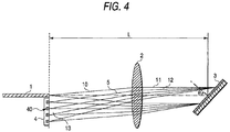
- the inventors have noted that the diffraction grating is a spectral element suitable for such a purpose and have disclosed, as a spectral branching module, a structure in which a diffraction grating 3 and a photodetector array 4 shown in Fig. 4 are combined (JP-W-WO99/46629).
- a light beam 10 having a wavelength multiplexed which is emitted from an optical fiber 1 is changed into a parallel light 11 through a collimator lens 2 and is incident on a diffraction grating 3.
- the light is divided through the diffraction grating 3 and is emitted at an output angle which is varied depending on a wavelength.
- An emitted light 12 passes through the collimator lens 2 again, thereby forming a focused beam spot group 13 on a photodetector array 4.
- Each photodetector 40 in the photodetector array 4 is provided in the position of the focused beam spot group 13 of a light having each wavelength (channel).
- ⁇ i ⁇ o (littrow arrangement).
- the above equation can be generally established also in the case of ⁇ i ⁇ ⁇ o . Accordingly, if a wavelength interval is constant, a plurality of photodetectors are arranged at an interval so that the position and wavelength (each channel) of the photodetector can be caused to correspond to each other with one to one.
- a communication wavelength in DWDM is defined to be a frequency pitch every 100 GHz at a minimum by the standard of the International Telecommunication Union (ITU).
- a position where the divided light beam reaches a light receiving surface is not provided at an interval (see a second row from the left in Table 1).
- frequency intervals between all the channels do not need to be constant.
- a "jump" is caused in the position where the divided light beam might further reach the light receiving surface in addition to the reasons described above.
- a conventional ordinary photodetector array has a constant pitch between the photodetectors.
- the photodetector cannot be caused to correspond to each channel with one to one so that a signal for one channel is received by the adjacent photodetectors or some photodetector elements do not receive a signal. Therefore, there is a problem in that a correspondence relationship between the photoreceptor and the channel becomes complicated and more photodetectors than channels are required for signal separation between the channels.
- the area of a photodetector chip is increased corresponding to the presence of the unused photodetector on a chip.
- a photodetector array in which three or more photodetectors are arranged rectilinearly and an array pitch between the adjacent photodetectors is not constant through the whole array.
- the size of a photodetector array chip can be substantially reduced by changing an array pitch between the photodetectors according to the position of incidence of a light on the photodetector array.
- Fig. 1 is a schematic view showing an optical communication monitor module 100 according to the invention.
- An incident light 110 having a wavelength multiplexed is led into a housing 200 of the module through an optical fiber 101 and is shaped into a beam having a predetermined diameter through a collimator lens 102.
- a position is adjusted such that a light is incident on a diffraction grating 103 at a predetermined angle. Consequently, an output angle is changed slightly and gradually for each channel having a wavelength varied so that a light 112 is emitted.
- the light 112 is caused to pass through a return collective lens 108 by means of a mirror 106. Consequently, a beam is collected on a photodetector array 140.
- each element interval of the photodetector array 140 is determined by the following equation, it is possible to form a channel monitor having a high degree of separation.
- a wavelength of 1.55 ⁇ m band is used.
- a central wavelength is defined to be 1552.52 nm.
- a channel pitch is set to 100 GHz according to the standard of a C band of the ITU and 16 continuous channels are used.
- An optical path length L is determined such that an interval in the photodetector array is 50 ⁇ m in the vicinity of the central wavelength.
- a diffraction order of the diffraction grating is set to 25 and a grating period is determined to be 24.7 ⁇ m such that an incidence angle is 71.5 degrees and an output angle is 38.5 degrees with a central wavelength.
- an interval between the photodetectors i.e.
- a photodetector pitch corresponding to an output angle from the diffraction grating of a light having each wavelength (channel) is shown in the Table 1.
- L is 48 mm.
- the interval between the photodetectors (the photodetector pitch) makes a difference of 1.4 ⁇ m (2.8 %) on both ends (i.e. between the maximum and minimal values).
- a photomask of the photodetector array having the photodetectors provided at the interval (the photodetector pitch) shown in the Table 1 is designed, a mesa photodetector array comprising InGaAsP/InP can further be fabricated in a conventional process.
- Fig. 2 is a plan view showing a photodetector array chip 151 thus fabricated.
- Fig. 2 is a schematic view in which the size, interval (pitch) and the like of the photodetector are not accurate.
- 16 photodetectors 140 are formed on an InP substrate 150, and are connected to bonding pads 160 through metallic wirings 170, respectively. The bonding pad usually requires a size of 80 to 100 ⁇ m square.
- the interval between the photodetectors 140 (i.e. the photodetector pitch) is approximately 50 ⁇ m which is smaller than that between the bonding pads 160.
- the bonding pads 160 are arranged in two rows on one of sides of the photodetectors 140. The way of the arrangement is not restricted thereto but the bonding pads 160 may be arranged as two rows each being located at a respective one of sides of the photodetectors 140, for example.
- various channel monitors such as 8-channel or 32-channel can be constituted.
- the photodetectors 140 are arrayed to accurately meet the photodetector pitch shown in the table 1.
- a difference in the interval between the photodetectors (i.e. in the photodetectorpitch) due to the selected wavelengths falls within 2.8%, and therefore problems rarely arise on actual working conditions even if all the photodetectors 140 are arrayed in an equal pitch.
- a width of the photodetector may also be varied according to a ratio of the interval (the pitch) between the photodetectors.
- While 16 continuous channels are used in the first embodiment, they may be divided into two parts, that is, 8 channels in each part for use, for example. Moreover, a frequency interval does not need to be 100 GHz. In the embodiment, an unused band for 1 THz is provided in the middle between two parts each having a frequency interval of 200 GHz (see the Table 1). In this case, a "jump" of approximately 250 ⁇ m (for four elements) is generated on the center at an interval between the photodetectors 140 as shown in the Table 1.
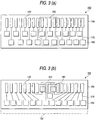
- Fig. 3(a) shows an example in which photodetectors are also formed in the jump portion to construct a photodetector array chip 152 having the same structure as that of the first embodiment. A portion surrounded by a broken line indicates an unused portion 220, and the photodetectors 140 and the bonding pads 160 in this portion are not used.
- bonding pads and wirings which are annexed thereto can also be omitted. If the interval between the photodetectors 140 (i.e. the photodetector pitch) is set to approximately 50 ⁇ m in the same manner as that in the first embodiment, it is preferable that the bonding pads 160 should be arranged in two rows in the structure of Fig. 3(a). On the other hand, if the four photodetectors 142 are omitted as shown in Fig. 3(b), several bonding pads can be provided in an empty space. In the example of the arrangement shown in Fig.
- bonding pads 162 for three elements are arranged in the empty space so that residual bonding pads 164 can be arranged in one row. For this reason, the area of a chip 153 can be more reduced than a chip 152 (shown in a one-dotted chain line) by 10% or more, and the size of a photodetector array chip can be reduced.
- the arrangement of the bonding pad shown in Fig. 3(b) is only illustrative and is not restricted thereto, and various structures can be supposed.
- the frequency interval is 200 GHz which is a double of that in the first embodiment. Therefore, if the interval between the photodetectors (the photodetector pitch) is approximately 50 ⁇ m in the same manner as in the first embodiment, the optical path length L may be approximately 24 mm which is approximately a half of that in the first embodiment.
- the photodetectors 140 are arrayed to accurately meet the photodetector pitch shown in table 1.
- a difference in the interval between the photodetectors (i.e. in the photodetector pitch) due to the selected wavelengths within each of divided two parts is not so large, and therefore problems rarely arise on actual working conditions even if the photodetectors 140 within each part are arrayed in an equal pitch.
- a width of the photodetector may also be varied according to a ratio of the interval (the pitch) between the photodetectors.
- a channel In a channel monitor module using a diffraction grating, a channel can be caused to correspond to a photodetector with one to one even if a wavelength of the channel does not have an equal interval, and the structure of the module can be simplified. Moreover, the size of a photodetector array chip can be reduced. Frequency Wavelength Embodiment 1 Embodiment 2 Channel 1 Wavelength Interval.
Landscapes
- Physics & Mathematics (AREA)
- Spectroscopy & Molecular Physics (AREA)
- General Physics & Mathematics (AREA)
- Optics & Photonics (AREA)
- Optical Communication System (AREA)
- Optical Couplings Of Light Guides (AREA)
- Light Receiving Elements (AREA)
- Solid State Image Pick-Up Elements (AREA)
Abstract
Description
| | Wavelength | Embodiment | 1 | | |||||
| | Wavelength Interval. | Output Angle | Photodetector Pitch Pi | Channel 1 | Wavelength Interval | Output Angle | Photodetector Pitch Pi | ||
| (THz) | (µm) | Δ λ i(nm) | oi(°) | (µm) | Δλi(nm) | oi(°) | (µm) | ||
| 196.1 | 1.52877 | ||||||||
| 196.0 | 1.52955 | ||||||||
| 195.9 | 1.53033 | 16 | 36.91 | ||||||
| 195.8 | 1.53112 | ||||||||
| 195.7 | 1.53190 | 15 | 1.56 | 37.02 | 48.1 | ||||
| 195.6 | 1.53268 | ||||||||
| 195.5 | 1.53347 | 14 | 1.57 | 37.14 | 48.3 | ||||
| 195.4 | 1.53425 | ||||||||
| 195.3 | 1.53504 | 13 | 1.57 | 37.25 | 48.4 | ||||
| 195.2 | 1.53582 | ||||||||
| 195.1 | 1.53561 | 12 | 1.57 | 37.37 | 48.6 | ||||
| 195.0 | 1.53740 | ||||||||
| 194.9 | 1.53819 | 11 | 1.58 | 37.48 | 48.8 | ||||
| 194.8 | 1.53898 | ||||||||
| 194.7 | 1.53977 | 10 | 1.58 | 37.60 | 49.0 | ||||
| 194.6 | 1.54056 | ||||||||
| 194.5 | 1.54135 | 9 | 1.58 | 37.71 | 49.1 | ||||
| 194.4 | 1.54214 | ||||||||
| 194.3 | 1.54294 | (1.59) | (37.83) | (49.3) | |||||
| 194.2 | 1.54373 | ||||||||
| 194.1 | 1.54453 | (1.59) | (37.95) | (49.5) | |||||
| 194.0 | 1.54532 | ||||||||
| 193.9 | 1.54612 | (1.59) | (38.06) | (49.7) | |||||
| 193.8 | 1.54692 | 16 | 38.12 | ||||||
| 193.7 | 1.54772 | 15 | 0.80 | 38.18 | 49.4 | (1.60) | (38.18) | (49.9) | |
| 193.6 | 1.54851 | 14 | 0.80 | 38.24 | 49.5 | ||||
| 193.5 | 1.54932 | 13 | 0.80 | 38.30 | 49.6 | 8 | 7.97 | 38.30 | 249.2 |
| 193.4 | 1.55012 | 12 | 0.80 | 38.36 | 49.7 | (1.60) | (50.0) | ||
| 193.3 | 1.55092 | 11 | 0.80 | 38.42 | 49.8 | 7 | 1.60 | 38.42 | 50.2 |
| 193.2 | 1.55172 | 10 | 0.80 | 38.48 | 49.9 | ||||
| 193.1 | 1.55252 | 9 | 0.80 | 38.54 | 50.0 | 6 | 1.61 | 38.54 | 50.4 |
| 193.0 | 1.55333 | 8 | 0.81 | 38.60 | 50.1 | ||||
| 192.9 | 1.55413 | 7 | 0.81 | 38.66 | 50.2 | 5 | 1.61 | 38.66 | 50.6 |
| 192.8 | 1.55494 | 6 | 0.81 | 38.72 | 50.3 | ||||
| 192.7 | 1.55575 | 5 | 0.81 | 38.78 | 50.4 | 4 | 1.61 | 38.78 | 50.8 |
| 192.6 | 1.55655 | 4 | 0.81 | 33.84 | 50.5 | ||||
| 192.5 | 1.55736 | 3 | 0.81 | 38.90 | 50.6 | 3 | 1.62 | 33.90 | 51.0 |
| 192.4 | 1.55817 | 2 | 0.81 | 38.96 | 50.7 | ||||
| 192.3 | 1.55898 | 1 | 0.81 | 39.02 | 50.8 | 2 | 1.62 | 39.02 | 51.2 |
| 192.2 | 1.55979 | ||||||||
| 192.1 | 1.56061 | 1 | 1.62 | 39.14 | 51.4 |
Claims (6)
- A photodetector array having three or more photodetectors arranged rectilinearly, wherein an array pitch between the adjacent photodetectors is not constant through the whole array.
- An optical communication monitor module for dividing a wavelength multiplexed light having N channels (N is an integer of 3 or more) through a diffraction grating having a diffraction order of m and a grating period of d and for receiving the divided light through a photodetector array,
wherein a pitch pi between i'th and (i + 1)'th (i is an integer of 1 to (N - 1)) photodetectors in the photodetector array satisfies the following equation: - A photodetector array chip comprising:wherein at least one of the bonding pads is disposed on the row of the photodetectors and between adjacent two of the photodetectors.photodetectors arrayed in a row; andbonding pads respectively connected to the photodetectors through wirings;
- The photodetector array chip according to claim 3, wherein the majority of the bonding pads are arranged in a row.
- The photodetector array chip according to claim 3, wherein an array pitch between the adjacent photodetectors is not constant through the whole array.
- The photodetector array chip according to claim 3, wherein:the photodetector array chip is used for an optical module for dividing a wavelength multiplexed light having N channels (N is an integer of 3 or more) through a diffraction grating having a diffraction order of m and a grating period of d; anda pitch pi between i'th and (i + 1) 'th (i is an integer of 1 to (N - 1)) photodetectors in the photodetector array satisfies the following equation:Δλi being a wavelength interval between i'th and (i+1)'th channels, L being an optical path length between the diffraction grating and the photodetector array, and o being a mean output angle.
Applications Claiming Priority (2)
| Application Number | Priority Date | Filing Date | Title |
|---|---|---|---|
| JP2000234941A JP2002050778A (en) | 2000-08-02 | 2000-08-02 | Light receiving element array and optical communication monitor module using the same |
| JP2000234941 | 2000-08-02 |
Publications (2)
| Publication Number | Publication Date |
|---|---|
| EP1178535A2 true EP1178535A2 (en) | 2002-02-06 |
| EP1178535A3 EP1178535A3 (en) | 2008-07-16 |
Family
ID=18727232
Family Applications (1)
| Application Number | Title | Priority Date | Filing Date |
|---|---|---|---|
| EP01117793A Withdrawn EP1178535A3 (en) | 2000-08-02 | 2001-08-02 | Photodetector array and optical communication monitoring |
Country Status (6)
| Country | Link |
|---|---|
| US (1) | US6690002B2 (en) |
| EP (1) | EP1178535A3 (en) |
| JP (1) | JP2002050778A (en) |
| CN (1) | CN1238907C (en) |
| CA (1) | CA2354350A1 (en) |
| TW (1) | TW531988B (en) |
Families Citing this family (34)
| Publication number | Priority date | Publication date | Assignee | Title |
|---|---|---|---|---|
| AU3032700A (en) | 1999-01-08 | 2000-07-24 | Ibsen Micro Structures A/S | Spectrometer |
| JP2002198544A (en) * | 2000-12-26 | 2002-07-12 | Nippon Sheet Glass Co Ltd | Photodetector and optical demultiplexer using it |
| US6978062B2 (en) | 2001-02-21 | 2005-12-20 | Ibsen Photonics A/S | Wavelength division multiplexed device |
| US6842239B2 (en) | 2001-08-10 | 2005-01-11 | Ibsen Photonics A/S | Alignment of multi-channel diffractive WDM device |
| US7085492B2 (en) * | 2001-08-27 | 2006-08-01 | Ibsen Photonics A/S | Wavelength division multiplexed device |
| US6888681B2 (en) | 2002-01-31 | 2005-05-03 | Nippon Sheet Glass Co., Ltd. | Optical demultiplexer |
| US7034739B2 (en) * | 2002-04-05 | 2006-04-25 | Osepchuk John M | Delivery of quasi-periodic pulses of EM energy utilizing the principle of beating-wave amplification |
| KR100571019B1 (en) | 2004-01-15 | 2006-04-13 | 삼성전자주식회사 | Photosensitive compound for photoresist layer adhesion and method of forming photoresist pattern using the same |
| US7538945B2 (en) * | 2005-01-07 | 2009-05-26 | Nippon Sheet Glass Company, Limited | Optical path changing module |
| JP2006343223A (en) * | 2005-06-09 | 2006-12-21 | Yokogawa Electric Corp | Photodiode array |
| US7805081B2 (en) * | 2005-08-11 | 2010-09-28 | Pacific Biosciences Of California, Inc. | Methods and systems for monitoring multiple optical signals from a single source |
| US7715001B2 (en) | 2006-02-13 | 2010-05-11 | Pacific Biosciences Of California, Inc. | Methods and systems for simultaneous real-time monitoring of optical signals from multiple sources |
| US7692783B2 (en) * | 2006-02-13 | 2010-04-06 | Pacific Biosciences Of California | Methods and systems for simultaneous real-time monitoring of optical signals from multiple sources |
| US7995202B2 (en) * | 2006-02-13 | 2011-08-09 | Pacific Biosciences Of California, Inc. | Methods and systems for simultaneous real-time monitoring of optical signals from multiple sources |
| US8207509B2 (en) | 2006-09-01 | 2012-06-26 | Pacific Biosciences Of California, Inc. | Substrates, systems and methods for analyzing materials |
| WO2008028160A2 (en) * | 2006-09-01 | 2008-03-06 | Pacific Biosciences Of California, Inc. | Substrates, systems and methods for analyzing materials |
| US20080080059A1 (en) * | 2006-09-28 | 2008-04-03 | Pacific Biosciences Of California, Inc. | Modular optical components and systems incorporating same |
| US20100167413A1 (en) * | 2007-05-10 | 2010-07-01 | Paul Lundquist | Methods and systems for analyzing fluorescent materials with reduced autofluorescence |
| US20080277595A1 (en) * | 2007-05-10 | 2008-11-13 | Pacific Biosciences Of California, Inc. | Highly multiplexed confocal detection systems and methods of using same |
| JP2008292924A (en) * | 2007-05-28 | 2008-12-04 | Nippon Telegr & Teleph Corp <Ntt> | Optical signal processing device |
| JP4842915B2 (en) * | 2007-11-16 | 2011-12-21 | 日本電信電話株式会社 | Optical channel monitor and wavelength selective optical switch |
| DK3629011T3 (en) | 2008-09-16 | 2024-01-29 | Pacific Biosciences California Inc | INTEGRATED OPTICAL DEVICE |
| EP3460458B1 (en) | 2010-02-19 | 2021-08-11 | Pacific Biosciences of California, Inc. | A method for nucleic acid sequencing |
| US8994946B2 (en) | 2010-02-19 | 2015-03-31 | Pacific Biosciences Of California, Inc. | Integrated analytical system and method |
| US9372308B1 (en) | 2012-06-17 | 2016-06-21 | Pacific Biosciences Of California, Inc. | Arrays of integrated analytical devices and methods for production |
| EP2936222B1 (en) | 2012-12-18 | 2019-07-03 | Pacific Biosciences Of California, Inc. | An optical analytical device |
| EP2959283B1 (en) | 2013-02-22 | 2022-08-17 | Pacific Biosciences of California, Inc. | Integrated illumination of optical analytical devices |
| CN107003241B (en) | 2014-08-27 | 2022-01-11 | 加利福尼亚太平洋生物科学股份有限公司 | Integrated analytical device array |
| US10487356B2 (en) | 2015-03-16 | 2019-11-26 | Pacific Biosciences Of California, Inc. | Integrated devices and systems for free-space optical coupling |
| US11983790B2 (en) | 2015-05-07 | 2024-05-14 | Pacific Biosciences Of California, Inc. | Multiprocessor pipeline architecture |
| EP4425153A3 (en) | 2015-06-12 | 2024-11-20 | Pacific Biosciences Of California, Inc. | Integrated target waveguide devices and systems for optical coupling |
| CN106784028B (en) * | 2016-12-29 | 2021-04-13 | 北京邮电大学 | A subwavelength beam splitting grating hybrid integrated photodetector array |
| AU2021222009A1 (en) | 2020-02-18 | 2022-09-15 | Pacific Biosciences Of California, Inc. | Highly multiplexed nucleic acid sequencing systems |
| US12535417B2 (en) | 2021-05-04 | 2026-01-27 | Pacific Biosciences Of California, Inc. | Arrays of integrated analytical devices with reduced-scale unit cell |
Family Cites Families (6)
| Publication number | Priority date | Publication date | Assignee | Title |
|---|---|---|---|---|
| US4736360A (en) | 1986-07-21 | 1988-04-05 | Polaroid Corporation | Bulk optic echelon multi/demultiplexer |
| US5020910A (en) * | 1990-03-05 | 1991-06-04 | Motorola, Inc. | Monolithic diffraction spectrometer |
| US5731874A (en) * | 1995-01-24 | 1998-03-24 | The Board Of Trustees Of The Leland Stanford Junior University | Discrete wavelength spectrometer |
| US6256016B1 (en) * | 1997-06-05 | 2001-07-03 | Logitech, Inc. | Optical detection system, device, and method utilizing optical matching |
| TW468062B (en) * | 1998-03-11 | 2001-12-11 | Nippon Sheet Glass Co Ltd | Optical demultiplexer |
| EP1156311A1 (en) * | 1999-10-08 | 2001-11-21 | Nippon Sheet Glass Co., Ltd. | Photodetector array and optical branching filter using the array |
-
2000
- 2000-08-02 JP JP2000234941A patent/JP2002050778A/en not_active Withdrawn
-
2001
- 2001-07-27 US US09/915,477 patent/US6690002B2/en not_active Expired - Fee Related
- 2001-07-31 CA CA002354350A patent/CA2354350A1/en not_active Abandoned
- 2001-08-01 CN CNB011238259A patent/CN1238907C/en not_active Expired - Fee Related
- 2001-08-02 TW TW090118856A patent/TW531988B/en not_active IP Right Cessation
- 2001-08-02 EP EP01117793A patent/EP1178535A3/en not_active Withdrawn
Also Published As
| Publication number | Publication date |
|---|---|
| EP1178535A3 (en) | 2008-07-16 |
| CN1238907C (en) | 2006-01-25 |
| JP2002050778A (en) | 2002-02-15 |
| CA2354350A1 (en) | 2002-02-02 |
| US6690002B2 (en) | 2004-02-10 |
| CN1336740A (en) | 2002-02-20 |
| TW531988B (en) | 2003-05-11 |
| US20020050557A1 (en) | 2002-05-02 |
Similar Documents
| Publication | Publication Date | Title |
|---|---|---|
| US6690002B2 (en) | Photodetector array and optical communication monitor module using the same | |
| US7085492B2 (en) | Wavelength division multiplexed device | |
| US6304692B1 (en) | Echelle grating dense wavelength division multiplexer/demultiplexer with two dimensional single channel array | |
| US6978062B2 (en) | Wavelength division multiplexed device | |
| US5355237A (en) | Wavelength-division multiplexed optical integrated circuit with vertical diffraction grating | |
| US7151635B2 (en) | Planar waveguide reflective diffraction grating | |
| US6373606B1 (en) | Optical demultiplexer | |
| US5973838A (en) | Apparatus which includes a virtually imaged phased array (VIPA) in combination with a wavelength splitter to demultiplex wavelength division multiplexed (WDM) light | |
| US9369201B2 (en) | Integrated multi-channel wavelength monitor | |
| EP1059545A1 (en) | Arrayed waveguide grating multiplexer and demultiplexer | |
| EP0231874B1 (en) | Optical wavelength compounding/dividing device | |
| KR100566853B1 (en) | Apparatus which includes a virtually images phased array (vipa) in combination with a wavelength splitter to demultiplex a wavelength division multiplexed (wdm) light | |
| US7304797B2 (en) | Inputs and outputs for an optical multiplexer/demultiplexer utilizing the grating facet diffraction envelope | |
| US7209612B2 (en) | Two-stage optical bi-directional transceiver | |
| WO2001086848A1 (en) | Optical wavelength division multiplexer and de-multiplexer | |
| US20030048498A1 (en) | Optical performance monitor | |
| US7587112B2 (en) | Optical device and light control method | |
| US6424760B1 (en) | Optical multiplexer/demultiplexer | |
| JP4456065B2 (en) | Arrayed waveguide grating circuit | |
| US6574397B2 (en) | Optical multiplexer/demultiplexer | |
| KR100341388B1 (en) | Intergrated optic wavelength monitoring device | |
| KR20070022709A (en) | 2 stage optical bidirectional transceiver | |
| WO2003024011A2 (en) | Optical performance monitor |
Legal Events
| Date | Code | Title | Description |
|---|---|---|---|
| PUAI | Public reference made under article 153(3) epc to a published international application that has entered the european phase |
Free format text: ORIGINAL CODE: 0009012 |
|
| AK | Designated contracting states |
Kind code of ref document: A2 Designated state(s): AT BE CH CY DE DK ES FI FR GB GR IE IT LI LU MC NL PT SE TR |
|
| AX | Request for extension of the european patent |
Free format text: AL;LT;LV;MK;RO;SI |
|
| RIC1 | Information provided on ipc code assigned before grant |
Ipc: H01L 27/144 20060101ALI20080303BHEP Ipc: H04B 10/06 20060101ALI20080303BHEP Ipc: H01L 27/146 20060101AFI20011123BHEP |
|
| PUAL | Search report despatched |
Free format text: ORIGINAL CODE: 0009013 |
|
| AK | Designated contracting states |
Kind code of ref document: A3 Designated state(s): AT BE CH CY DE DK ES FI FR GB GR IE IT LI LU MC NL PT SE TR |
|
| AX | Request for extension of the european patent |
Extension state: AL LT LV MK RO SI |
|
| AKX | Designation fees paid | ||
| STAA | Information on the status of an ep patent application or granted ep patent |
Free format text: STATUS: THE APPLICATION IS DEEMED TO BE WITHDRAWN |
|
| 18D | Application deemed to be withdrawn |
Effective date: 20090117 |
|
| REG | Reference to a national code |
Ref country code: DE Ref legal event code: 8566 |