EP1178399A1 - Saturation in an arithmetic unit - Google Patents
Saturation in an arithmetic unit Download PDFInfo
- Publication number
- EP1178399A1 EP1178399A1 EP00410091A EP00410091A EP1178399A1 EP 1178399 A1 EP1178399 A1 EP 1178399A1 EP 00410091 A EP00410091 A EP 00410091A EP 00410091 A EP00410091 A EP 00410091A EP 1178399 A1 EP1178399 A1 EP 1178399A1
- Authority
- EP
- European Patent Office
- Prior art keywords
- unit
- values
- range
- result
- bits
- Prior art date
- Legal status (The legal status is an assumption and is not a legal conclusion. Google has not performed a legal analysis and makes no representation as to the accuracy of the status listed.)
- Granted
Links
Images


Classifications
-
- G—PHYSICS
- G06—COMPUTING OR CALCULATING; COUNTING
- G06F—ELECTRIC DIGITAL DATA PROCESSING
- G06F7/00—Methods or arrangements for processing data by operating upon the order or content of the data handled
- G06F7/38—Methods or arrangements for performing computations using exclusively denominational number representation, e.g. using binary, ternary, decimal representation
- G06F7/48—Methods or arrangements for performing computations using exclusively denominational number representation, e.g. using binary, ternary, decimal representation using non-contact-making devices, e.g. tube, solid state device; using unspecified devices
- G06F7/544—Methods or arrangements for performing computations using exclusively denominational number representation, e.g. using binary, ternary, decimal representation using non-contact-making devices, e.g. tube, solid state device; using unspecified devices for evaluating functions by calculation
- G06F7/5443—Sum of products
-
- G—PHYSICS
- G06—COMPUTING OR CALCULATING; COUNTING
- G06F—ELECTRIC DIGITAL DATA PROCESSING
- G06F7/00—Methods or arrangements for processing data by operating upon the order or content of the data handled
- G06F7/38—Methods or arrangements for performing computations using exclusively denominational number representation, e.g. using binary, ternary, decimal representation
- G06F7/48—Methods or arrangements for performing computations using exclusively denominational number representation, e.g. using binary, ternary, decimal representation using non-contact-making devices, e.g. tube, solid state device; using unspecified devices
- G06F7/499—Denomination or exception handling, e.g. rounding or overflow
- G06F7/49905—Exception handling
- G06F7/4991—Overflow or underflow
- G06F7/49921—Saturation, i.e. clipping the result to a minimum or maximum value
Definitions
- the present invention relates to an arithmetic unit and in particular but not exclusively to an arithmetic unit for use in a digital signal processor.
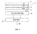
- FIG. 1 shows a block diagram of an arithmetic unit 2 which is able to add together two partial products P1 and P2 and the accumulator.
- the arithmetic unit 2 has a first register 4 which stores the value P1 and a second register 6 which stores the value P2.
- P1 + P2 X * Y.
- the current accumulator ACCU is stored in a third register 8.
- two further steps are carried out.
- the three vectors P1, P2 and the accumulator ACCU are reduced to two vectors through a carry save adder stage 10.
- the carry save adder stage 10 actually comprises a number of individual 3 to 2 carry save adders each of which provides two outputs. One of those outputs is a sum output and the other output is a carry output.
- the number of carry save adders making up the carry save adder stage will at least be equal to the number of bits of the register P1, the register P2 or the accumulator ACCU.
- each individual carry save adder provides two outputs, a carry output and a sum output. As there are several carry save adders in parallel, a sum vector and a carry vector are obtained. These vectors are input to a global adder 12. The global adder 12 provides the result RES.
- the result RES may fall outside a permitted range of values.
- an arithmetic unit for adding a plurality of values to define a result
- said arithmetic unit comprising means for receiving said plurality of values; means for adding said plurality of values to define a result, said- result being within a first range; means for determining if said result fall within a second range, said second range being smaller than the first range; and means for modifying said result in so that the result output by said arithmetic unit falls within the second range.
- the output of the arithmetic unit always falls within the second range.
- the result falls outside the second range, the result is sometimes referred to as having overflowed.
- it is modified to fall inside the second range, it is referred to as being clamped or saturated.
- three values may be added together. Two of those values may be a partial product whilst the third of those values may be an accumulation result.
- the arithmetic unit embodying the present invention can be used for multiply accumulate functions.
- the adding means may comprise a carry save adder.
- the carry save adder may comprise a plurality of 3 to 2 carry save adders.
- the adding means may comprise an adder stage for providing said result.
- the adder stage may add the two outputs of the carry save adder stage to provide a single result.
- the determining means may be arranged to take into account the bits other than the considered bits. Only some of the bits of each of the plurality of values may be used perform a predecoding as to whether or not the result falls outside the second range. A bit generated by the addition of all the other bits of the plurality of values may also be used. This bit may enable the achievement of decoding as to whether or not the result falls outside the second range. This may take the form of a carry.
- the second range can be expressed by N bits and bits N, N-1 and possibly the N-2 of at least some of the plurality of values may be considered.
- the number of bits which are considered may depend on the number of values, the range of each value and/or the required range of the final result.
- the arithmetic unit may be arranged to operate in 2's complement binary arithmetic. This means that positive and negative numbers can be represented.
- a first of the plurality of values may have an N bit format and may fall in the range -2 N-1 to 2 N-1 -1.
- the sum of a second and a third of the plurality of values may fall in the range of -2 N-1 to 2 N-1 .
- the first range may be -2 N to 2 N -1 and the second range may be -2 N-1 to 2 N-1 -1.
- a round may be introduced when generating first and second partial product values. This round may-consist of adding 2 N/2-1 to the result so that the first range may be -2 N to 2 N -1 + 2 (N/2)-1 .
- the determining means may consider bits N down to N-2 where three values are used.
- a first carry save addition of bits N-2, a second carry save addition of bits N-1 of all of said plurality of values and a third carry save-addition of bits N from two of said plurality of values and bit N-1 from a further one of said plurality of values may be considered by the determining means.
- the further one of the plurality of values may be an accumulator value whilst the other two values may be partial product values. Bits of significance greater than or equal to N-1 only, resulting form the three carry save additions may be taken into account by the determining means and may be added together by a fourth addition.
- a fifth addition may be performed between the resulting bits and a carry generated by the additions of bits N-2 down to 0 of the three values. If the result of the fifth addition has first and second bits which are different, then said result falls outside said second range. If the first and second bits are the same, then the result falls within the second range.
- the calculation generating the carry used in the fifth addition may be performed in the same way as described previously. First a carry save addition may be performed on the three values. Then the resulting two values may be added together in a final addition.
- the carry used by the determining means may be the one out column N-2 of the final addition.
- the means for modifying the result may be arranged to receive information as to the sign of the total of two of said plurality of values and information as to one bit of a further one of said values to determine if the result can fall out of said second range at the positive end thereof or the negative end thereof.
- the modifying means may modify the result to have a maximum positive or maximum negative value of said second range depending on which end of the second range the result can fall out of and if the result is determined to fall outside said second range.
- a plurality of registers may be provided for storing said plurality of values.
- X and Y are initially multiplied to generate two partial products P1 and P2.
- the generation of two partial products from two numbers multiplied together is well known in the'art and will not be described further here.
- the result of the multiplication P is defined as being equal to P1+P2.
- a first register 14 is provided for storing the first partial product P1 and a second register 16 is provided for storing the second partial product P2. 2's complement arithmetic is used.
- the first bit of a signed number indicates if the number is positive or negative. The usual convention is that if the first bit has the value "1" then the number is a negative number whereas if the first bit has the value "0", then the number is a positive number.
- a third register 18 is provided for the current accumulator ACCU.
- the third register 18 stores a N-bit value.
- the value of the N bit data will fall in the range of -2 N-1 to 2 N-1 -1, as it is expressed in 2's complement arithmetic.
- P1 may be a N+2 bit negative value and P2 may be a N+3 bit positive value.
- P1 and P2 can have other formats. P1 and P2 are such that their sum always falls within the range -2 N-1 to 2 N-1 .
- the final result will be in the range -2 N to 2 N -1.
- a round may also be performed on the final result.
- the N/2 least significant bits can be cleared.
- a round is -performed by adding 2 (N/2)-1 to the partial products and then clearing the N/2 least significant bits from the result RES. Clearing the N/2 least significant bits can be equated to setting those bits to "0".
- the final result, after rounding, will therefore be in the range of -2 N to 2 N +2 (N/2-1) -1.
- saturation has to be performed in order to keep the result within the range -2 N-1 to 2 N-1 -1.
- the circuitry for ensuring that the result is saturated or is within the required range will be described in more detail hereinafter.
- the output of the first second and third registers 14, 16 and 18 are input to a carry save adder stage 20.
- the carry save adder stage comprises a number of 3 to 2 carry save adders.
- the number of carry save adders may be equal to N+1.
- N carry save adders are required if N bits of the accumulator ACCU are taken into account.
- One further carry save adder is required if overflow detection is considered.
- Each carry save adder receives one input from each of the three registers 14, 16 and 18 and provides a carry output and a sum output.
- Each of these carry and sum outputs are input to a global adder stage 22.
- the global adder stage 22 comprises a number of adders each of which adds a carry output and a sum output to provide a respective one of the bits of the result.
- Numbers in the first range -2 N to 2 N +2 (N/2-1) -1 are expressed on N+2 bits, that is bit 0 to bit N+1. To write down the most positive values in the range requires N+2 bits.
- Numbers in the second range -2 N-1 to 2 N-1 -1 are expressed on N bits, that is bit 0 to bit N-1.
- bits N+1, N and N-1 should be checked. However, embodiments of the present invention are able to suppress the check on bit N+1.
- the partial products P1 and-P2 are used as is the accumulator ACCU.
- the accumulator ACCU has a N bit format, that is it can be expressed on N bits, that is 0 to N-1.
- Bit N is a copy of bit N-1 obtained by carrying out a sign extension. In Figure 3, only bits N, N-1 and N-2 are shown.
- a carry save adder stage 100 enables P1, P2 and ACCU to be reduced to a sum vector and a carry vector.
- Carry(N-1) is generated by the carry save adder 100 receiving bits N-2 from the two partial products P1 and P2 and bit N-2 from the accumulator ACCU.
- Sum(N-1) and carry(N) are generated by the carry save adder receiving bits N-1 from the partial products P1 and P2 and ACCU.
- Sum (N) is generated by the carry save adder 100 receiving the bit N from the two partial products P1 and P2 and bit N-1 from ACCU.
- Carry (N), Carry (N-1), Sum (N) and Sum (N-1) are added together to generate SN-1 and SN.
- the carry from the previous column N-2 is taken into account and is added to S(N-1).
- This carry CN-2 is the carry generated out of- column N-2 when performing the addition of Sum (N-2 down to 0) and Carry (N-2 down to 0).
- bits N and N-1 of the result of the multiply accumulate function are obtained. These bits are compared. If they are not equal, there is an overflow as explained above.
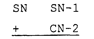
- SN and SN-1 are first calculated, without taking into account CN-2. According to the values SN and SN-1, it is defined which values of CN-2 give an overflow.
- the carry save adder stage 20 will add bits N-1 from the first to third registers 14 to 18 to provide a sum output Sum (N-1) and a carry output Carry(N) as illustrated in Figure 3 by arrows A and B respectively. These values are output to the global adder 22 and also to a calculation unit 24 via inputs 32 and 34.. Bits N-2 from the first, second and third registers 14 to 18 are summed to provide the carry output Carry(N-1). The bit Carry (N-1) is transmitted to the detection unit 24 via line 32.
- the calculation unit 24 also receives the following inputs: bit N from the first register 14 via line 26, bit N from the second register 16 via line 28 and bit N-1 of the third register 18 via line 30.
- Bit N-1 of the third register is taken into account instead of bit N. This is because this register is the accumulator and only N bits of the accumulator are taken into account.
- Bit N, that is the N+1 bit is a sign extension and so is a copy of bit N-1. Using these values, the calculation unit is able to calculate the values SN and SN-1.
- SN-1 is the sum of Sum(N-1) from the carry save adder stage and the Carry(N-1) from the carry save adder stage.
- Value SN is the sum of Sum(N), Carry(N) and the carry resulting from the summing of Sum(N-1) and Carry(N-1).
- Sum (N) is calculated in the calculation unit 24 by adding bit N from the first and second registers and bit N-1 of the third register.
- Carry (N)- is from the carry save adder stage 20.
- the calculation unit 24 provides two outputs.
- the first output 36 Satif0 will be high to indicate that saturation is required if the carry CN-2 is zero whereas the second output 38 Satif1 will be high to indicate that saturation will occur if the carry CN-2 is 1.
- SN and SN-1 are both 0, then a high output will be provided via the second output Satif1.
- SN is 0 and SN-1 is 1, then a high output will be provided on both the Satif0 output 36 and the Satif1 output 38 as an overflow will always be provided regardless of the value of the carry CN-2.
- SN has the value 1 and SN-1 is equal to 0, then a high output will be provided on the first output SatifO 36 as an overflow will be provided if the carry CN-2 is zero.
- SN and SN-1 are both 1, then a zero output is provided via the first and second output Satif0 or Satif1 as no overflow will occur.
- the first .and second outputs 36 and 38 are input to a first multiplexer which is controlled by the carry CN-2 which is output from the global adder 22. If there is saturation, the output of the first multiplexer 40 provides a high signal to a second multiplexer 42 from which ever of the first and second outputs 36 and 38 of the calculation units 24 is high. In particular, if the carry value CN-2 is 1, then the second output 38 Satif1 will be output by the first multiplexer 40. If the carry value CN-2 is 0, then the first output 36 Satif0 will be output by the first multiplexer 40. If there is no saturation, then the first multiplexer 40 provides a zero output to the second multiplexer 42.
- not(satif0) and not(satif1) are generated instead of satif0 and satif1 respectively.
- This provides a saturation signal which is the opposite to that of the arrangement described previously.
- This signal has the value 1 if there is no overflow and 0 if there is an overflow.
- the correct output of the multiplexer 42 is obtained by permutation the inputs of the multiplexer.
- the result value is connected on input '1' of the multiplexer 42 and Sat_val is connected to input '0' of multiplexer 42. This way, when the signal has the value 0 and there is an overflow, the output of the multiplexer 42 is Sat_val.
- the output of the multiplexer is the Res value.
- the saturation unit 44 receives three inputs 46 to 50.
- the first input 46 provides bit N-1 of the third register 18.
- the second input 48 provides the sign of the sum of P1+P2.
- the third input 50 provides an indication as to whether or not a round takes place. When a round is performed, the N/2 least significant bits are cleared. summarises whether or not a positive or negative overflow takes place.
- the type of overflow condition (positive overflow, negative overflow or no possible overflow) can be determined. If the accumulation value ACCU and the product P are greater than zero, a positive overflow is possible. If the accumulation value ACCU and the product P are both less than zero, a negative overflow is possible. If the accumulation value ACCU and the product P have the opposite sign, then overflow is not possible without rounding. If rounding does take place then positive overflow may occur.
- the saturation unit 44 provides the saturation value 52 according to the inputs 46, 48 and 50. When a negative overflow is possible, the value 52 is -2 N-1 . When a positive overflow is possible and there is no rounding, the value 52 is 2 N-1 -1. When a positive overflow is possible and there is rounding, the value 52 is 2 N-1 -2 N/2 .
- the output 52 of the saturation unit 44 is input to the second multiplexer 42 along with the output from the global adder stage 22. If an overflow has occurred as determined by the calculation unit 24, the saturation value will replace the result RES output by the global adder stage 22. If, on the other hand, saturation is not required, then the result RES of the global adder stage 22 will be output by the second multiplexer 42.
- the output of the first multiplexer 40 will control the output of the second multiplexer 42 to select either the output of the saturation unit 44 or the output of the global adder stage 22 depending on whether or not the result determined by the global adder stage 22 fall within or outside the permitted range.
- the result RES is replaced by the saturation value. If a negative overflow occurs, that is the result RES is below the minimum value -2 N-1 , then the saturation value is the minimum value that can be expressed in N bits in 2's complement arithmetic, that is -2 N-1 . If a positive overflow occurs, that is the result RES is greater than the maximum value 2 N-1 -1, the saturation value is the maximum positive value 2 N-1 -1 if no round has to be performed or if a round has to be performed, the maximum positive value with the N/2 least significant bits cleared, that is 2 N-1 -2 N/2. Thus it is possible to perform all the overflow detection calculation in parallel with the calculation of the result RES (and the carry CN-2).
- embodiments of the present invention can be incorporated in a digital signal processor. Embodiments of the present invention can be incorporated in an integrated circuit.
Landscapes
- Engineering & Computer Science (AREA)
- Physics & Mathematics (AREA)
- General Physics & Mathematics (AREA)
- Theoretical Computer Science (AREA)
- Computational Mathematics (AREA)
- Computing Systems (AREA)
- Mathematical Analysis (AREA)
- Mathematical Optimization (AREA)
- Pure & Applied Mathematics (AREA)
- General Engineering & Computer Science (AREA)
- Complex Calculations (AREA)
Abstract
Description
- The present invention relates to an arithmetic unit and in particular but not exclusively to an arithmetic unit for use in a digital signal processor.
- In known arithmetic units, it is possible to calculate a multiply accumulate function. In a multiply accumulate function, a first number X is multiplied by a second number Y and added to an accumulator ACCU. In mathematical notation, the result RES of this function can be represented as follows: RES=ACCU+X*Y.
- Reference is made to Figure 1 which shows a block diagram of an
arithmetic unit 2 which is able to add together two partial products P1 and P2 and the accumulator. Thearithmetic unit 2 has afirst register 4 which stores the value P1 and asecond register 6 which stores the value P2. When X is multiplied by Y, two partial products P1 and P2 result, with P1 + P2 = X * Y. These values P1 and P2 are stored in the first andsecond registers - The current accumulator ACCU is stored in a
third register 8. In order to obtain the result RES, two further steps are carried out. The three vectors P1, P2 and the accumulator ACCU are reduced to two vectors through a carrysave adder stage 10. The carrysave adder stage 10 actually comprises a number of individual 3 to 2 carry save adders each of which provides two outputs. One of those outputs is a sum output and the other output is a carry output. The number of carry save adders making up the carry save adder stage will at least be equal to the number of bits of the register P1, the register P2 or the accumulator ACCU. - As discussed hereinbefore, each individual carry save adder provides two outputs, a carry output and a sum output. As there are several carry save adders in parallel, a sum vector and a carry vector are obtained. These vectors are input to a
global adder 12. Theglobal adder 12 provides the result RES. - When the first value P1, the second value P2 and the third value ACCU are added together, the result RES may fall outside a permitted range of values.
- It is therefore an aim of embodiments of the present invention to ensure that the final result is within a permitted range of values.
- According to one aspect of the present invention, there is provided an arithmetic unit for adding a plurality of values to define a result, said arithmetic unit comprising means for receiving said plurality of values; means for adding said plurality of values to define a result, said- result being within a first range; means for determining if said result fall within a second range, said second range being smaller than the first range; and means for modifying said result in so that the result output by said arithmetic unit falls within the second range.
- In this way, it can be ensured that the output of the arithmetic unit always falls within the second range. When the result falls outside the second range, the result is sometimes referred to as having overflowed. When it is modified to fall inside the second range, it is referred to as being clamped or saturated.
- In one embodiment of the present invention, three values may be added together. Two of those values may be a partial product whilst the third of those values may be an accumulation result.
- Accordingly, the arithmetic unit embodying the present invention can be used for multiply accumulate functions.
- The adding means may comprise a carry save adder. The carry save adder may comprise a plurality of 3 to 2 carry save adders. The adding means may comprise an adder stage for providing said result. The adder stage may add the two outputs of the carry save adder stage to provide a single result.
- The determining means may be arranged to take into account the bits other than the considered bits. Only some of the bits of each of the plurality of values may be used perform a predecoding as to whether or not the result falls outside the second range. A bit generated by the addition of all the other bits of the plurality of values may also be used. This bit may enable the achievement of decoding as to whether or not the result falls outside the second range. This may take the form of a carry.
- The second range can be expressed by N bits and bits N, N-1 and possibly the N-2 of at least some of the plurality of values may be considered. The number of bits which are considered may depend on the number of values, the range of each value and/or the required range of the final result.
- The arithmetic unit may be arranged to operate in 2's complement binary arithmetic. This means that positive and negative numbers can be represented.
- A first of the plurality of values may have an N bit format and may fall in the range -2N-1 to 2N-1-1. The sum of a second and a third of the plurality of values may fall in the range of -2N-1 to 2N-1. The first range may be -2N to 2N-1 and the second range may be -2N-1 to 2N-1-1. A round may be introduced when generating first and second partial product values. This round may-consist of adding 2N/2-1 to the result so that the first range may be -2N to 2N-1 + 2(N/2)-1.
- The determining means may consider bits N down to N-2 where three values are used. A first carry save addition of bits N-2, a second carry save addition of bits N-1 of all of said plurality of values and a third carry save-addition of bits N from two of said plurality of values and bit N-1 from a further one of said plurality of values may be considered by the determining means. The further one of the plurality of values may be an accumulator value whilst the other two values may be partial product values. Bits of significance greater than or equal to N-1 only, resulting form the three carry save additions may be taken into account by the determining means and may be added together by a fourth addition. A fifth addition may be performed between the resulting bits and a carry generated by the additions of bits N-2 down to 0 of the three values. If the result of the fifth addition has first and second bits which are different, then said result falls outside said second range. If the first and second bits are the same, then the result falls within the second range.
- The calculation generating the carry used in the fifth addition may be performed in the same way as described previously. First a carry save addition may be performed on the three values. Then the resulting two values may be added together in a final addition. The carry used by the determining means may be the one out column N-2 of the final addition.
- The means for modifying the result may be arranged to receive information as to the sign of the total of two of said plurality of values and information as to one bit of a further one of said values to determine if the result can fall out of said second range at the positive end thereof or the negative end thereof. The modifying means may modify the result to have a maximum positive or maximum negative value of said second range depending on which end of the second range the result can fall out of and if the result is determined to fall outside said second range.
- A plurality of registers may be provided for storing said plurality of values.
- For a better understanding of the present invention and as to how the same may be carried into effect, reference will now be made by way of example to the accompanying drawings in which:-
- Figure 1 shows a known arithmetic unit;
- Figure 2 shows a block diagram of an arithmetic unit embodying the present invention; and
- Figure 3 illustrates the calculation performed by the arithmetic unit. The embodiment shown in Figure 2 is arranged to carry out a multiply accumulate function where RES=ACCU+X*Y. As discussed in relation to the figure 1, X is the number to be multiplied and Y is the multiplier. ACCU is the accumulator value which may be increasing or decreasing and RES is the result of the function.
-
- X and Y are initially multiplied to generate two partial products P1 and P2. The generation of two partial products from two numbers multiplied together is well known in the'art and will not be described further here. The result of the multiplication P, is defined as being equal to P1+P2.
- As with the arithmetic unit shown in Figure 1, a
first register 14 is provided for storing the first partial product P1 and asecond register 16 is provided for storing the second partial product P2. 2's complement arithmetic is used. The first bit of a signed number indicates if the number is positive or negative. The usual convention is that if the first bit has the value "1" then the number is a negative number whereas if the first bit has the value "0", then the number is a positive number. - A
third register 18 is provided for the current accumulator ACCU. Thethird register 18 stores a N-bit value. The value of the N bit data will fall in the range of -2N-1 to 2N-1-1, as it is expressed in 2's complement arithmetic. - The product P resulting from the sum of P1+P2 will be in the range -2N-1 to 2N-1. P1 may be a N+2 bit negative value and P2 may be a N+3 bit positive value. However P1 and P2 can have other formats. P1 and P2 are such that their sum always falls within the range -2N-1 to 2N-1.
- When the N least significant bits of the accumulator are added to the product P, the final result will be in the range -2N to 2N-1.
- A round may also be performed on the final result. In other words, the N/2 least significant bits can be cleared. In one embodiment of the present invention, a round is -performed by adding 2(N/2)-1 to the partial products and then clearing the N/2 least significant bits from the result RES. Clearing the N/2 least significant bits can be equated to setting those bits to "0".
- The final result, after rounding, will therefore be in the range of -2N to 2N+2(N/2-1)-1. However, saturation has to be performed in order to keep the result within the range -2N-1 to 2N-1-1. The circuitry for ensuring that the result is saturated or is within the required range will be described in more detail hereinafter.
- The output of the first second and
third registers save adder stage 20. As with-the arithmetic unit-of Figure 1, the carry save adder stage comprises a number of 3 to 2 carry save adders. The number of carry save adders may be equal to N+1. N carry save adders are required if N bits of the accumulator ACCU are taken into account. One further carry save adder is required if overflow detection is considered. Each carry save adder receives one input from each of the threeregisters global adder stage 22. Theglobal adder stage 22 comprises a number of adders each of which adds a carry output and a sum output to provide a respective one of the bits of the result. - The principal behind overflow decoding will now be discussed. The maximum value is 2N+2(N/2-1)-1, before saturation.- In 2's complement arithmetic, this value is expressed by N+2 bits. The minimum before saturation is -2N which can be expressed in N+1 bits.
- One way of identifying that saturation is required will be described with reference to Figure 3. Numbers in the first range -2N to 2N+2(N/2-1)-1 are expressed on N+2 bits, that is
bit 0 to bit N+1. To write down the most positive values in the range requires N+2 bits. Numbers in the second range -2N-1 to 2N-1-1 are expressed on N bits, that isbit 0 to bit N-1. - To check if there is-an overflow the following bits are checked:
- bits greater than bit N-1 are equal to bit N-1 if the number is in the second range. The bits N-1 and greater should be checked; and
- bits over bit N+1, that is the N+2th bit as bits are counted from 0, will always be the same if the number is in the first range.
-
- It is therefore not necessary to check bits over bit N+1. Bits N+1, N and N-1 should be checked. However, embodiments of the present invention are able to suppress the check on bit N+1. A very few number of values actually require the N+2 bit format in the first range. These values are the ones in the
range 2N to 2N-1+2N/2-1. These values have the property that bits N+1, N and N-1 have thevalues range 2N to 2N-1+2N/2-1. - For the other values of the first range, that is values in the range -2N to 2N-1, these are expressed on N+1 bits only, that is
bits 0 to N. It is therefore sufficient -to check bits N-1 and N. - Reference is made to Figure 3 which shows how these principles can be applied in embodiments of the present invention. The partial products P1 and-P2 are used as is the accumulator ACCU. The accumulator ACCU has a N bit format, that is it can be expressed on N bits, that is 0 to N-1. Bit N is a copy of bit N-1 obtained by carrying out a sign extension. In Figure 3, only bits N, N-1 and N-2 are shown.
- A carry
save adder stage 100 enables P1, P2 and ACCU to be reduced to a sum vector and a carry vector. - The values of interest are Carry(N-1), Sum(N-1), Carry (N) and Sum (N). Carry(N-1) is generated by the
carry save adder 100 receiving bits N-2 from the two partial products P1 and P2 and bit N-2 from the accumulator ACCU. - Sum(N-1) and carry(N) are generated by the carry save adder receiving bits N-1 from the partial products P1 and P2 and ACCU.
- Sum (N) is generated by the
carry save adder 100 receiving the bit N from the two partial products P1 and P2 and bit N-1 from ACCU. - Carry (N), Carry (N-1), Sum (N) and Sum (N-1) are added together to generate SN-1 and SN. The carry from the previous column N-2 is taken into account and is added to S(N-1). This carry CN-2 is the carry generated out of- column N-2 when performing the addition of Sum (N-2 down to 0) and Carry (N-2 down to 0).
- When performing the additionthe bits N and N-1 of the result of the multiply accumulate function are obtained. These bits are compared. If they are not equal, there is an overflow as explained above. To speed up detection, SN and SN-1 are first calculated, without taking into account CN-2. According to the values SN and SN-1, it is defined which values of CN-2 give an overflow.
- The carry
save adder stage 20 will add bits N-1 from the first tothird registers 14 to 18 to provide a sum output Sum (N-1) and a carry output Carry(N) as illustrated in Figure 3 by arrows A and B respectively. These values are output to theglobal adder 22 and also to acalculation unit 24 viainputs third registers 14 to 18 are summed to provide the carry output Carry(N-1).The bit Carry (N-1) is transmitted to thedetection unit 24 vialine 32. - The
calculation unit 24 also receives the following inputs: bit N from thefirst register 14 vialine 26, bit N from thesecond register 16 vialine 28 and bit N-1 of thethird register 18 vialine 30. Bit N-1 of the third register is taken into account instead of bit N. This is because this register is the accumulator and only N bits of the accumulator are taken into account. Bit N, that is the N+1 bit is a sign extension and so is a copy of bit N-1. Using these values, the calculation unit is able to calculate the values SN and SN-1. SN-1 is the sum of Sum(N-1) from the carry save adder stage and the Carry(N-1) from the carry save adder stage. Value SN is the sum of Sum(N), Carry(N) and the carry resulting from the summing of Sum(N-1) and Carry(N-1). Sum (N) is calculated in thecalculation unit 24 by adding bit N from the first and second registers and bit N-1 of the third register. Carry (N)-is from the carrysave adder stage 20. - Reference is made to the table 1 which summarises the cases where an overflow will occur.
SN SN-1 OVERFLOW 0 0 Overflow if CN-2='1' 0 1 Always overflow 1 0 Overflow if CN-2='0' 1 1 No overflow - The
calculation unit 24 provides two outputs. Thefirst output 36 Satif0 will be high to indicate that saturation is required if the carry CN-2 is zero whereas thesecond output 38 Satif1 will be high to indicate that saturation will occur if the carry CN-2 is 1. If SN and SN-1 are both 0, then a high output will be provided via the second output Satif1. If SN is 0 and SN-1 is 1, then a high output will be provided on both theSatif0 output 36 and theSatif1 output 38 as an overflow will always be provided regardless of the value of the carry CN-2. If SN has thevalue 1 and SN-1 is equal to 0, then a high output will be provided on thefirst output SatifO 36 as an overflow will be provided if the carry CN-2 is zero. Finally, if SN and SN-1 are both 1, then a zero output is provided via the first and second output Satif0 or Satif1 as no overflow will occur. - The first .and
second outputs global adder 22. If there is saturation, the output of thefirst multiplexer 40 provides a high signal to asecond multiplexer 42 from which ever of the first andsecond outputs calculation units 24 is high. In particular, if the carry value CN-2 is 1, then thesecond output 38 Satif1 will be output by thefirst multiplexer 40. If the carry value CN-2 is 0, then thefirst output 36 Satif0 will be output by thefirst multiplexer 40. If there is no saturation, then thefirst multiplexer 40 provides a zero output to thesecond multiplexer 42. - In summary, satif1=not(SN) and satif0=SN XOR SN-1 where XOR is an exclusive or function.
- If sat=0, then the
multiplexer 42 will output the Res value. If sat=1, then there is an overflow and the value out of themultiplexer 42 is the saturation value generated byunit 44. - In an alternative embodiment of the present invention, not(satif0) and not(satif1) are generated instead of satif0 and satif1 respectively. This provides a saturation signal which is the opposite to that of the arrangement described previously. This signal has the
value 1 if there is no overflow and 0 if there is an overflow. The correct output of themultiplexer 42 is obtained by permutation the inputs of the multiplexer. The result value is connected on input '1' of themultiplexer 42 and Sat_val is connected to input '0' ofmultiplexer 42. This way, when the signal has thevalue 0 and there is an overflow, the output of themultiplexer 42 is Sat_val. When the signal has thevalue 1 and there is no overflow, then the output of the multiplexer is the Res value. - Once detection of an overflow or saturation situation has occurred, it is necessary to define the saturation value which should replace the actual calculated value. Overflow occurs when the result RES falls outside the permitted range. In the case of a negative value, the saturation value will be -2N-1. In the case of a positive value, the saturation value will be 2N-1-1. This is determined by the
saturation unit 44. Thesaturation unit 44 receives threeinputs 46 to 50. Thefirst input 46 provides bit N-1 of thethird register 18. Thesecond input 48 provides the sign of the sum of P1+P2. Thethird input 50 provides an indication as to whether or not a round takes place. When a round is performed, the N/2 least significant bits are cleared.summarises whether or not a positive or negative overflow takes place. ACCU and P sign No round performed Round performed (adding 2(N/2)-1) ACCU>0, P>0 Positive OVF Positive OVF ACCU<0, P<0 Negative OVF Negative OVF ACCU>0, P<0 No possible OVF Positive OVF ACCU<0, P>0 No possible OVF Positive OVF - Taking into account the range of the accumulator value and of the product P, the sign of the two data and if a round is performed, the type of overflow condition (positive overflow, negative overflow or no possible overflow) can be determined. If the accumulation value ACCU and the product P are greater than zero, a positive overflow is possible. If the accumulation value ACCU and the product P are both less than zero, a negative overflow is possible. If the accumulation value ACCU and the product P have the opposite sign, then overflow is not possible without rounding. If rounding does take place then positive overflow may occur. The
saturation unit 44 provides thesaturation value 52 according to theinputs value 52 is -2N-1. When a positive overflow is possible and there is no rounding, thevalue 52 is 2N-1 -1. When a positive overflow is possible and there is rounding, thevalue 52 is 2N-1-2N/2. - The
output 52 of thesaturation unit 44 is input to thesecond multiplexer 42 along with the output from theglobal adder stage 22. If an overflow has occurred as determined by thecalculation unit 24, the saturation value will replace the result RES output by theglobal adder stage 22. If, on the other hand, saturation is not required, then the result RES of theglobal adder stage 22 will be output by thesecond multiplexer 42. The output of thefirst multiplexer 40 will control the output of thesecond multiplexer 42 to select either the output of thesaturation unit 44 or the output of theglobal adder stage 22 depending on whether or not the result determined by theglobal adder stage 22 fall within or outside the permitted range. - When an overflow occurs, the result RES is replaced by the saturation value. If a negative overflow occurs, that is the result RES is below the minimum value -2N-1, then the saturation value is the minimum value that can be expressed in N bits in 2's complement arithmetic, that is -2N-1. If a positive overflow occurs, that is the result RES is greater than the maximum value 2N-1-1, the saturation value is the maximum positive value 2N-1-1 if no round has to be performed or if a round has to be performed, the maximum positive value with the N/2 least significant bits cleared, that is 2N-1-2N/2. Thus it is possible to perform all the overflow detection calculation in parallel with the calculation of the result RES (and the carry CN-2). Then the final detection of the overflow can be obtained as soon as CN-2 is available. It is done this way, because CN-2 gives the ability to take into account bits N-2 down to 0 of the operands, but it is the latest available signal required for overflow detection.
- In alternative embodiments of the present invention, it is possible to perform the same saturation detection using other signals from the
registers 14 to 16, the carry save adder stage, or the global adder. - It should be appreciated that embodiments of the present invention can be incorporated in a digital signal processor. Embodiments of the present invention can be incorporated in an integrated circuit.
Claims (23)
- An arithmetic unit for adding a plurality of values to define a result, said arithmetic unit comprising:means for receiving said plurality of values;means for adding said plurality of values to define a result, said result being within a first range;means for determining if said result fall within a second range, said second range-being smaller than the first range, said means being arranged to consider only some of the bits of said result; andmeans for modifying said result in so that the result output by said arithmetic unit falls within the second range.
- A unit as claimed in claim 1, wherein three values are added together.
- A unit as claimed in claim 1 or 2, wherein said adding means comprises a carry save adder stage.
- A unit as claimed in claims 2 and 3, wherein said carry save adder stage comprises a plurality of 3 to 2 carry save adders.
- A unit as claimed in any of claims 1 to 4, wherein said adding means comprises an adder stage for providing said result.
- A unit as claimed in any preceding claim wherein said determining means is arranged to take into account the bits other than the considered bits.
- A unit as claimed in any preceding claim, wherein the second range can be expressed by N bits and bits N toN-2 of at least some of the plurality of values are considered by said determining means.
- A unit as claimed in any preceding claim, wherein the arithmetic unit is arranged to operate in 2's complement binary arithmetic.
- A unit as claimed in claim 8, wherein a first of said plurality of values has an N bit format and falls in the range 2N-1 to 2N-1-1.
- A unit as claimed in claim 8 or 9, wherein the sum of a second and a third of said plurality of values falls in the range -2N-1 to 2N-1 + 2(N/2-1).
- A unit as claimed in claim 8, 9 or 10, wherein said first range is -2N to 2N + 2(N/2-1)-1 and said second range is -2N-1 to 2N- 1-1.
- A unit as claimed in any preceding claim wherein if it is determined that the result falls outside said second range, the result is replaced by a saturation value.
- A unit as claimed in claim 12, wherein a first saturation value is provided if one end of the range is exceeded and another saturation value is provided if the other end of the range is exceeded.
- A unit as claimed in claim 2 or any claim appended thereto,
wherein at least one of the following values is calculated;a first carry value is generated from bits N-2 from said three values;a second carry value is generated from the bits N-1 of said three values;a first sum value is generated from the bits N-1 of said three values; anda second sum is generated from the bits N of two of said values and bit N-1 of one of the values. - A unit as claimed in claim 14, wherein said first and second carry values and said first and second sums are generated to provide first and second result values.
- A unit as claimed in claim 15, wherein it is determined by said determining means if the second range is exceeded based on said first and second results and a third carry value.
- A unit as claimed in claim 16, wherein said third carry value is determined from an addition of a sum and a carry value for bits N-2 down to 0 of said values
- A unit as claimed in any preceding claim wherein a round is performed to clear the x least significant bits of said result.
- A unit as claimed in any preceding claim, wherein a round is performed by adding 2(N/2)-1 to said result.
- A -unit as claimed in any one of the preceding claims, wherein said means for modifying said result is arranged to receive information as to the sign of the total of a first and a second value and information as to one bit of a third value to determine if the result can fall out of said second range at the positive end thereof or the negative end thereof.
- A unit as claimed in any preceding claim, wherein said plurality of values comprise a plurality of partial products.
- A unit as claimed in any preceding claim, wherein said plurality of values comprise an accumulator.
- An unit as claimed in any preceding claim, wherein a plurality of registers are provided for storing said plurality of values.
Priority Applications (3)
| Application Number | Priority Date | Filing Date | Title |
|---|---|---|---|
| DE60015119T DE60015119D1 (en) | 2000-08-01 | 2000-08-01 | Saturation in an arithmetic unit |
| EP00410091A EP1178399B1 (en) | 2000-08-01 | 2000-08-01 | Saturation in an arithmetic unit |
| US09/919,482 US6983300B2 (en) | 2000-08-01 | 2001-07-30 | Arithmetic unit |
Applications Claiming Priority (1)
| Application Number | Priority Date | Filing Date | Title |
|---|---|---|---|
| EP00410091A EP1178399B1 (en) | 2000-08-01 | 2000-08-01 | Saturation in an arithmetic unit |
Publications (2)
| Publication Number | Publication Date |
|---|---|
| EP1178399A1 true EP1178399A1 (en) | 2002-02-06 |
| EP1178399B1 EP1178399B1 (en) | 2004-10-20 |
Family
ID=8174043
Family Applications (1)
| Application Number | Title | Priority Date | Filing Date |
|---|---|---|---|
| EP00410091A Expired - Lifetime EP1178399B1 (en) | 2000-08-01 | 2000-08-01 | Saturation in an arithmetic unit |
Country Status (3)
| Country | Link |
|---|---|
| US (1) | US6983300B2 (en) |
| EP (1) | EP1178399B1 (en) |
| DE (1) | DE60015119D1 (en) |
Families Citing this family (42)
| Publication number | Priority date | Publication date | Assignee | Title |
|---|---|---|---|---|
| US7467176B2 (en) | 2004-02-20 | 2008-12-16 | Altera Corporation | Saturation and rounding in multiply-accumulate blocks |
| US8620980B1 (en) | 2005-09-27 | 2013-12-31 | Altera Corporation | Programmable device with specialized multiplier blocks |
| US8266198B2 (en) * | 2006-02-09 | 2012-09-11 | Altera Corporation | Specialized processing block for programmable logic device |
| US8041759B1 (en) | 2006-02-09 | 2011-10-18 | Altera Corporation | Specialized processing block for programmable logic device |
| US8301681B1 (en) | 2006-02-09 | 2012-10-30 | Altera Corporation | Specialized processing block for programmable logic device |
| US8266199B2 (en) * | 2006-02-09 | 2012-09-11 | Altera Corporation | Specialized processing block for programmable logic device |
| US8386550B1 (en) | 2006-09-20 | 2013-02-26 | Altera Corporation | Method for configuring a finite impulse response filter in a programmable logic device |
| US8386553B1 (en) | 2006-12-05 | 2013-02-26 | Altera Corporation | Large multiplier for programmable logic device |
| US7930336B2 (en) | 2006-12-05 | 2011-04-19 | Altera Corporation | Large multiplier for programmable logic device |
| US8650231B1 (en) | 2007-01-22 | 2014-02-11 | Altera Corporation | Configuring floating point operations in a programmable device |
| US8645450B1 (en) | 2007-03-02 | 2014-02-04 | Altera Corporation | Multiplier-accumulator circuitry and methods |
| US8959137B1 (en) | 2008-02-20 | 2015-02-17 | Altera Corporation | Implementing large multipliers in a programmable integrated circuit device |
| US8307023B1 (en) | 2008-10-10 | 2012-11-06 | Altera Corporation | DSP block for implementing large multiplier on a programmable integrated circuit device |
| US8706790B1 (en) | 2009-03-03 | 2014-04-22 | Altera Corporation | Implementing mixed-precision floating-point operations in a programmable integrated circuit device |
| US8468192B1 (en) | 2009-03-03 | 2013-06-18 | Altera Corporation | Implementing multipliers in a programmable integrated circuit device |
| US8645449B1 (en) | 2009-03-03 | 2014-02-04 | Altera Corporation | Combined floating point adder and subtractor |
| US8650236B1 (en) | 2009-08-04 | 2014-02-11 | Altera Corporation | High-rate interpolation or decimation filter in integrated circuit device |
| US8412756B1 (en) | 2009-09-11 | 2013-04-02 | Altera Corporation | Multi-operand floating point operations in a programmable integrated circuit device |
| US8396914B1 (en) | 2009-09-11 | 2013-03-12 | Altera Corporation | Matrix decomposition in an integrated circuit device |
| US8539016B1 (en) | 2010-02-09 | 2013-09-17 | Altera Corporation | QR decomposition in an integrated circuit device |
| US8601044B2 (en) * | 2010-03-02 | 2013-12-03 | Altera Corporation | Discrete Fourier Transform in an integrated circuit device |
| US8484265B1 (en) | 2010-03-04 | 2013-07-09 | Altera Corporation | Angular range reduction in an integrated circuit device |
| US8510354B1 (en) | 2010-03-12 | 2013-08-13 | Altera Corporation | Calculation of trigonometric functions in an integrated circuit device |
| US8539014B2 (en) * | 2010-03-25 | 2013-09-17 | Altera Corporation | Solving linear matrices in an integrated circuit device |
| US8589463B2 (en) | 2010-06-25 | 2013-11-19 | Altera Corporation | Calculation of trigonometric functions in an integrated circuit device |
| US8862650B2 (en) | 2010-06-25 | 2014-10-14 | Altera Corporation | Calculation of trigonometric functions in an integrated circuit device |
| US8577951B1 (en) | 2010-08-19 | 2013-11-05 | Altera Corporation | Matrix operations in an integrated circuit device |
| US8645451B2 (en) | 2011-03-10 | 2014-02-04 | Altera Corporation | Double-clocked specialized processing block in an integrated circuit device |
| US9600278B1 (en) | 2011-05-09 | 2017-03-21 | Altera Corporation | Programmable device using fixed and configurable logic to implement recursive trees |
| US8812576B1 (en) | 2011-09-12 | 2014-08-19 | Altera Corporation | QR decomposition in an integrated circuit device |
| US8949298B1 (en) | 2011-09-16 | 2015-02-03 | Altera Corporation | Computing floating-point polynomials in an integrated circuit device |
| US9053045B1 (en) | 2011-09-16 | 2015-06-09 | Altera Corporation | Computing floating-point polynomials in an integrated circuit device |
| US8762443B1 (en) | 2011-11-15 | 2014-06-24 | Altera Corporation | Matrix operations in an integrated circuit device |
| US8543634B1 (en) | 2012-03-30 | 2013-09-24 | Altera Corporation | Specialized processing block for programmable integrated circuit device |
| US9098332B1 (en) | 2012-06-01 | 2015-08-04 | Altera Corporation | Specialized processing block with fixed- and floating-point structures |
| US8996600B1 (en) | 2012-08-03 | 2015-03-31 | Altera Corporation | Specialized processing block for implementing floating-point multiplier with subnormal operation support |
| US9207909B1 (en) | 2012-11-26 | 2015-12-08 | Altera Corporation | Polynomial calculations optimized for programmable integrated circuit device structures |
| US9189200B1 (en) | 2013-03-14 | 2015-11-17 | Altera Corporation | Multiple-precision processing block in a programmable integrated circuit device |
| US9348795B1 (en) | 2013-07-03 | 2016-05-24 | Altera Corporation | Programmable device using fixed and configurable logic to implement floating-point rounding |
| US9684488B2 (en) | 2015-03-26 | 2017-06-20 | Altera Corporation | Combined adder and pre-adder for high-radix multiplier circuit |
| US10067744B2 (en) | 2016-12-08 | 2018-09-04 | International Business Machines Corporation | Overflow detection for sign-magnitude adders |
| US10942706B2 (en) | 2017-05-05 | 2021-03-09 | Intel Corporation | Implementation of floating-point trigonometric functions in an integrated circuit device |
Citations (2)
| Publication number | Priority date | Publication date | Assignee | Title |
|---|---|---|---|---|
| US4807175A (en) * | 1986-03-29 | 1989-02-21 | Kabushiki Kaisha Toshiba | Booth's multiplier |
| US5889689A (en) * | 1997-09-08 | 1999-03-30 | Lucent Technologies Inc. | Hierarchical carry-select, three-input saturation |
Family Cites Families (3)
| Publication number | Priority date | Publication date | Assignee | Title |
|---|---|---|---|---|
| US5164914A (en) * | 1991-01-03 | 1992-11-17 | Hewlett-Packard Company | Fast overflow and underflow limiting circuit for signed adder |
| JPH07168696A (en) * | 1993-10-19 | 1995-07-04 | Mitsubishi Electric Corp | Overflow and underflow processing circuit for binary adder |
| US6912560B2 (en) * | 2000-12-08 | 2005-06-28 | Agere Systems, Inc. | Adder with improved overflow flag generation |
-
2000
- 2000-08-01 EP EP00410091A patent/EP1178399B1/en not_active Expired - Lifetime
- 2000-08-01 DE DE60015119T patent/DE60015119D1/en not_active Expired - Lifetime
-
2001
- 2001-07-30 US US09/919,482 patent/US6983300B2/en not_active Expired - Lifetime
Patent Citations (2)
| Publication number | Priority date | Publication date | Assignee | Title |
|---|---|---|---|---|
| US4807175A (en) * | 1986-03-29 | 1989-02-21 | Kabushiki Kaisha Toshiba | Booth's multiplier |
| US5889689A (en) * | 1997-09-08 | 1999-03-30 | Lucent Technologies Inc. | Hierarchical carry-select, three-input saturation |
Non-Patent Citations (3)
| Title |
|---|
| "LOW COST OVERFLOW GENERATION DEVICE FOR A MULTIPLIER-ACCUMULATOR", IBM TECHNICAL DISCLOSURE BULLETIN,US,IBM CORP. NEW YORK, vol. 28, no. 5, 1 October 1985 (1985-10-01), pages 1976 - 1977, XP000715017, ISSN: 0018-8689 * |
| NADEHARA ET AL: "A low-power 32.bit RISC processor with signal processing capability and its multiply-adder", VLSI SIGNAL PROCESSING., vol. VIII, 18 September 1995 (1995-09-18), Sakai, Japan, pages 51 - 60, XP002159317 * |
| YADAV ET AL: "Parallel Saturating Fractional Arithmetic Units", PROCEEDINGS GREAT LAKES SYMPOSIUM ON VLSI., March 1999 (1999-03-01), Ann Arbor, Michigan, US, pages 214 - 217, XP000955521 * |
Also Published As
| Publication number | Publication date |
|---|---|
| US20020038202A1 (en) | 2002-03-28 |
| DE60015119D1 (en) | 2004-11-25 |
| EP1178399B1 (en) | 2004-10-20 |
| US6983300B2 (en) | 2006-01-03 |
Similar Documents
| Publication | Publication Date | Title |
|---|---|---|
| EP1178399B1 (en) | Saturation in an arithmetic unit | |
| US7668896B2 (en) | Data processing apparatus and method for performing floating point multiplication | |
| JP5069476B2 (en) | Special processing blocks for programmable logic devices | |
| US7395304B2 (en) | Method and apparatus for performing single-cycle addition or subtraction and comparison in redundant form arithmetic | |
| EP0472139B1 (en) | A floating-point processor | |
| EP0574018B1 (en) | Accumulating multiplication circuit executing a double precision multiplication at a high speed | |
| US6925480B2 (en) | Microarchitecture of an arithmetic unit | |
| US6754689B2 (en) | Method and apparatus for performing subtraction in redundant form arithmetic | |
| JPH01112332A (en) | Floating point unit combining multiplicative/arithmetic logic computation functions | |
| KR20060057574A (en) | Arithmetic unit and method for addition or subtraction by preliminary saturation test | |
| US5954790A (en) | Method and apparatus for parallel prediction and computation of massive cancellation in floating point subtraction | |
| US4639887A (en) | Bifurcated method and apparatus for floating point addition with decreased latency time | |
| US6947962B2 (en) | Overflow prediction algorithm and logic for high speed arithmetic units | |
| US20020184285A1 (en) | Floating point adder | |
| US4999800A (en) | Floating point adder with pre-shifter | |
| US20060036667A1 (en) | Methods and apparatus for an efficient floating point ALU | |
| US8015231B2 (en) | Data processing apparatus and method for performing floating point multiplication | |
| US6449629B1 (en) | Three input split-adder | |
| US5117384A (en) | Method and apparatus for exponent adder | |
| EP1296223A2 (en) | Adder incrementer circuit | |
| US5408427A (en) | Detection of exponent underflow and overflow in a floating point adder | |
| US7444366B2 (en) | Faster shift value calculation using modified carry-lookahead adder | |
| US7386580B2 (en) | Data processing apparatus and method for computing an absolute difference between first and second data elements | |
| US5208769A (en) | Unsigned integer multiply/divide circuit | |
| US7640286B2 (en) | Data processing apparatus and method for performing floating point multiplication |
Legal Events
| Date | Code | Title | Description |
|---|---|---|---|
| PUAI | Public reference made under article 153(3) epc to a published international application that has entered the european phase |
Free format text: ORIGINAL CODE: 0009012 |
|
| AK | Designated contracting states |
Kind code of ref document: A1 Designated state(s): AT BE CH CY DE DK ES FI FR GB GR IE IT LI LU MC NL PT SE Kind code of ref document: A1 Designated state(s): DE FR GB IT |
|
| AX | Request for extension of the european patent |
Free format text: AL;LT;LV;MK;RO;SI |
|
| 17P | Request for examination filed |
Effective date: 20020731 |
|
| AKX | Designation fees paid |
Free format text: DE FR GB IT |
|
| 17Q | First examination report despatched |
Effective date: 20030516 |
|
| GRAP | Despatch of communication of intention to grant a patent |
Free format text: ORIGINAL CODE: EPIDOSNIGR1 |
|
| GRAS | Grant fee paid |
Free format text: ORIGINAL CODE: EPIDOSNIGR3 |
|
| GRAA | (expected) grant |
Free format text: ORIGINAL CODE: 0009210 |
|
| AK | Designated contracting states |
Kind code of ref document: B1 Designated state(s): DE FR GB IT |
|
| PG25 | Lapsed in a contracting state [announced via postgrant information from national office to epo] |
Ref country code: IT Free format text: LAPSE BECAUSE OF FAILURE TO SUBMIT A TRANSLATION OF THE DESCRIPTION OR TO PAY THE FEE WITHIN THE PRESCRIBED TIME-LIMIT;WARNING: LAPSES OF ITALIAN PATENTS WITH EFFECTIVE DATE BEFORE 2007 MAY HAVE OCCURRED AT ANY TIME BEFORE 2007. THE CORRECT EFFECTIVE DATE MAY BE DIFFERENT FROM THE ONE RECORDED. Effective date: 20041020 |
|
| REG | Reference to a national code |
Ref country code: GB Ref legal event code: FG4D |
|
| REG | Reference to a national code |
Ref country code: IE Ref legal event code: FG4D |
|
| REF | Corresponds to: |
Ref document number: 60015119 Country of ref document: DE Date of ref document: 20041125 Kind code of ref document: P |
|
| PG25 | Lapsed in a contracting state [announced via postgrant information from national office to epo] |
Ref country code: DE Free format text: LAPSE BECAUSE OF FAILURE TO SUBMIT A TRANSLATION OF THE DESCRIPTION OR TO PAY THE FEE WITHIN THE PRESCRIBED TIME-LIMIT Effective date: 20050121 |
|
| PLBE | No opposition filed within time limit |
Free format text: ORIGINAL CODE: 0009261 |
|
| STAA | Information on the status of an ep patent application or granted ep patent |
Free format text: STATUS: NO OPPOSITION FILED WITHIN TIME LIMIT |
|
| 26N | No opposition filed |
Effective date: 20050721 |
|
| ET | Fr: translation filed | ||
| PGFP | Annual fee paid to national office [announced via postgrant information from national office to epo] |
Ref country code: FR Payment date: 20080828 Year of fee payment: 9 |
|
| PGFP | Annual fee paid to national office [announced via postgrant information from national office to epo] |
Ref country code: GB Payment date: 20080729 Year of fee payment: 9 |
|
| GBPC | Gb: european patent ceased through non-payment of renewal fee |
Effective date: 20090801 |
|
| REG | Reference to a national code |
Ref country code: FR Ref legal event code: ST Effective date: 20100430 |
|
| PG25 | Lapsed in a contracting state [announced via postgrant information from national office to epo] |
Ref country code: FR Free format text: LAPSE BECAUSE OF NON-PAYMENT OF DUE FEES Effective date: 20090831 |
|
| PG25 | Lapsed in a contracting state [announced via postgrant information from national office to epo] |
Ref country code: GB Free format text: LAPSE BECAUSE OF NON-PAYMENT OF DUE FEES Effective date: 20090801 |