EP1176860A2 - Shielded case, electronic device using shielded case, electronic apparatus using electronic device, and method for manufacturing shielded case - Google Patents
Shielded case, electronic device using shielded case, electronic apparatus using electronic device, and method for manufacturing shielded case Download PDFInfo
- Publication number
- EP1176860A2 EP1176860A2 EP01118141A EP01118141A EP1176860A2 EP 1176860 A2 EP1176860 A2 EP 1176860A2 EP 01118141 A EP01118141 A EP 01118141A EP 01118141 A EP01118141 A EP 01118141A EP 1176860 A2 EP1176860 A2 EP 1176860A2
- Authority
- EP
- European Patent Office
- Prior art keywords
- sections
- shielded
- shielded case
- case
- walls
- Prior art date
- Legal status (The legal status is an assumption and is not a legal conclusion. Google has not performed a legal analysis and makes no representation as to the accuracy of the status listed.)
- Granted
Links
- 238000000034 method Methods 0.000 title claims description 9
- 238000004519 manufacturing process Methods 0.000 title claims description 5
- 238000003466 welding Methods 0.000 claims abstract description 7
- 230000013011 mating Effects 0.000 claims description 44
- 238000005452 bending Methods 0.000 claims description 4
- 230000000694 effects Effects 0.000 description 7
- 230000010355 oscillation Effects 0.000 description 7
- 229910000679 solder Inorganic materials 0.000 description 7
- 239000000463 material Substances 0.000 description 5
- 230000010354 integration Effects 0.000 description 4
- 230000005540 biological transmission Effects 0.000 description 2
- 230000015572 biosynthetic process Effects 0.000 description 2
- 230000008878 coupling Effects 0.000 description 2
- 238000010168 coupling process Methods 0.000 description 2
- 238000005859 coupling reaction Methods 0.000 description 2
- 239000002184 metal Substances 0.000 description 2
- 229910052751 metal Inorganic materials 0.000 description 2
- 230000003287 optical effect Effects 0.000 description 2
- RYGMFSIKBFXOCR-UHFFFAOYSA-N Copper Chemical compound [Cu] RYGMFSIKBFXOCR-UHFFFAOYSA-N 0.000 description 1
- 229910052802 copper Inorganic materials 0.000 description 1
- 239000010949 copper Substances 0.000 description 1
- 238000005520 cutting process Methods 0.000 description 1
- 238000010586 diagram Methods 0.000 description 1
- 230000005670 electromagnetic radiation Effects 0.000 description 1
- 238000003912 environmental pollution Methods 0.000 description 1
- 239000007769 metal material Substances 0.000 description 1
- 238000012986 modification Methods 0.000 description 1
- 230000004048 modification Effects 0.000 description 1
- 230000000717 retained effect Effects 0.000 description 1
- 238000000926 separation method Methods 0.000 description 1
- 238000005476 soldering Methods 0.000 description 1
Images




Classifications
-
- H—ELECTRICITY
- H05—ELECTRIC TECHNIQUES NOT OTHERWISE PROVIDED FOR
- H05K—PRINTED CIRCUITS; CASINGS OR CONSTRUCTIONAL DETAILS OF ELECTRIC APPARATUS; MANUFACTURE OF ASSEMBLAGES OF ELECTRICAL COMPONENTS
- H05K5/00—Casings, cabinets or drawers for electric apparatus
- H05K5/06—Hermetically-sealed casings
-
- H—ELECTRICITY
- H05—ELECTRIC TECHNIQUES NOT OTHERWISE PROVIDED FOR
- H05K—PRINTED CIRCUITS; CASINGS OR CONSTRUCTIONAL DETAILS OF ELECTRIC APPARATUS; MANUFACTURE OF ASSEMBLAGES OF ELECTRICAL COMPONENTS
- H05K9/00—Screening of apparatus or components against electric or magnetic fields
Definitions
- the present invention relates to shielded cases designed to inhibit the transmission of electromagnetic waves, electronic devices using the shielded cases, electronic apparatuses using the electronic devices, and methods for manufacturing the shielded cases.
- Fig. 10 is a perspective view of a known shielded case 10 disclosed in, for example, Japanese Unexamined Patent Application Publication No. 2-52481.
- Shielded case 10 is made of a metal or an insulative material coated with a metallic film and includes a top wall 12, a front wall 14, a rear wall 16 and a pair of side walls 18 and 20.
- the bottom 22 of the shielded case 10 is designed to be mounted on a circuit board and is open.
- Shielded case 10 is formed by cutting a blank 24 (Fig. 3) having a predetermined shape from a single sheet of material and bending the sheet at substantially right angles along the dashed lines of Fig. 3 to form the walls 12 - 20.
- the two side walls 18, 20 are formed by half walls 18a, 18b, and 20a, 20b, respectively. Each of the half walls extends from and is integral with a respective edge of the front or rear walls 14, 16.
- Mating parts 18c and 18d are formed in the half walls 18a and 18b, respectively, and interlock with each other when assembled to form the side wall 18.
- mating parts 20c and 20d are formed in the half walls 20a and 20b and interlock with when assembled to form the side wall 20.
- the half walls 18a and 18b are butt-jointed at their respective edges in such a manner that the mating parts 18c and 18d couple with each other.
- the half walls 20a, 20b are butt-jointed at their respective edges in such a manner that the mating parts 20c and 20d couple with each other.
- An electronic element e.g., an oscillation circuit which is likely to be affected by electromagnetic waves is typically housed in the shielded case to protect it from externally generated electromagnetic waves and to contain electromagnetic waves generated by the electronic element with the case.
- Various types of electronic devices can be shielded using the foregoing shield.
- One such class of devices are sensors for determining the movement of an object (e.g., an oscillation gyro). Such sensors are subject to strong impacts which threaten the integrity of the shielded case.
- the two mating pairs of half walls of the known shielded case 10 are held together by the interlocking relationship between the mating parts 18c, 18d and 20c,20d,respectively. Because these mating parts only interlock with one another, there is a risk that they will separate when an external impact is applied to the shielded case. If this happens, a gap will be formed between the mating parts and the electronic element in the case will not be sufficiently shielded from electromagnetic waves.
- a shielded case comprises:
- half walls are firmly coupled with each other by forming depressions in the half walls, whereby the half walls are not likely to separate from each other when an impact is applied.
- the half walls can be firmly coupled with each other without using solder, whereby a product free from lead can be provided.
- the half walls are coupled with each other without gaps therebetween, whereby electromagnetic waves inside can be prevented from leaking to the outside and the outside electronic waves can be reliably shielded.
- the present invention is also directed towards a shielded electronic device comprising:
- half walls of a shielded case are firmly coupled with each other, whereby a risk in that the sidewalls remove from each other and an electronic element received in the shielded case is exposed to the outside when an impact is applied is avoided.
- An electronic circuit according to the present invention contains a plurality of components, at least one of said components being a shielded electronic device comprising:
- an electronic device in which a risk that the half walls of a shielded case will separate from each other and expose an electronic element received in the shielded case to external electromagnetic radiation when an impact is applied to the case is avoided.
- a method for manufacturing a shielded electronic device comprises:
- Fig. 1 is a perspective view of a shielded case according to a first embodiment of the present invention.
- Fig. 2 is a side view of the shielded case shown in Fig. 1.
- Fig. 3 is a development view of a blank from which the shielded case of both the invention and the prior art is formed.
- Fig. 4 is an enlarged view of a portion of the shielded case shown in Fig. 1.
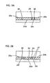
- Figs. 5A and 5B are sectional views taken along line 5-5 of Fig. 4.
- Figs. 6A, 6B, 6C, 6D, and 6E are side views of shielded cases according to alternative embodiments of the present invention.
- Fig. 7A is a side view of a shielded case according to another embodiment of the present invention.
- Fig. 7B is a development view of the blank form which the shielded case of Fig. 7A is formed.
- Fig. 8A is an exploded side view of an electronic device in which an electronic element is stored in the shielded case of Fig. 7A.
- Fig. 8B is a side view of the electronic device of Fig.8A with the electronic element housed in the shielded
- Fig. 9 is a block diagram of a circuit for avoiding the effects of manual movements of a camcorder using the shielded case of the present invention.
- Fig. 10 is a perspective view of a known shielded case.
- FIG. 1 A first embodiment of the present invention is shown in Figs. 1 through 5.
- the shielded case 10-1 of the invention includes a top wall 12, a front wall 14, a rear wall 16 and a pair of side walls 18, 20.
- the basic structure of the first embodiment of the present invention is substantially the same as the prior art and will not be described again.
- the primary difference between the prior art and the first embodiment of the invention is that the blank 24 is made of a ductile material which is expanded in the area of mating parts 18c, 18d, 20c and 20d by a series of deformations formed in the ductile material in the area of the mating parts. In the embodiment shown in Figs. 1 and 2, the deformations are circular depressions.
- the shielded case 10-1 of the invention is preferably formed from a single blank 14 shown in Fig. 3.
- the blank 14 is preferably cut from a ductile plate (such as copper) to ensure that the interlocking portions of the side wall will expand when the depressions 26 are formed therein.
- the ductile plate preferably has a predetermined thickness and the blank 14 is preferably cut using a press or the like.
- the blank 14 After the blank 14 has been cut, it is bent at substantially right angles along each of the dashed lines shown in Fig. 3 to form the walls 12 - 20 with the mating parts 18c, 18d and 20c and 20d interlocking with one another.
- the half walls 18a and 18b are butt-jointed at their respective edges to form the side wall 18
- the half walls 20a and 20b are butt-jointed at their respective edges to form the side wall 20.
- this is insufficient to avoid gapping between the adjacent half walls when a large external impact is applied to the case 10-1.
- the present invention forms deformations in the side walls in the area of the mating parts to pressure weld, and thereby securely couple, the half walls together.
- this is achieved by forming circular depressions in the half walls 18a, 18b and 20a, 20b in the areas of the mating parts 18c, 18d and 20c, 20d. These depressions are formed using a press or other suitable apparatus (or by hand). This simple method securely couples the half walls together and avoids the problems of the prior art without the use of solder.
- Fig. 4 is an enlarged view of a portion of the front wall 14 enclosed by a dotted line, of the shielded case 10 shown in Fig. 2.
- Fig. 5A is a sectional view along line 5-5 of the portion of the shielded case 10-1 shown in Fig. 4 before the depression 26 is formed.
- Fig. 5B is a sectional view along the line 5-5 of the portion of the shielded case 10-1 shown in Fig. 4, after the depression 26 has been formed.
- the mating portions 20c and 20d overlap each other in the area of the a 2-shaped interface 28 between the upper and lower half walls 20a and 20b.
- the depressions 26 are preferably formed in this overlapped area so that when the ductile material forming the case 10-1 expands (at least in the direction of the arrows in Fig. 4)the abutting portions of the Z-shaped interface 28 are forced into pressure contact with one another and are pressure-welded together. This effect can better be understood with reference to Figs. 5A and 5B.
- Fig. 5A the depression 26 has not yet been formed in the half wall 20b and there may be a small gap between the adjacent mating portions. Even if the mating portions are touching, they are not yet pressure welded.
- Fig. 5B shows the state of the mating portions once the depression 26 has been formed in the mating portion 20d. As shown by the arrows, the mating portion 20d expands outwardly toward the Z-shaped interface 28 causing the abutting edges to be pressure-welded. In the embodiment shown, the expansion caused by the depression 26 is large and projections 30 are created in the area of the Z-shaped interface 28. However, a smaller depression 26 can be formed so as to pressure-weld the abutting edges together without forming the projections 30.
- the foregoing process is preferably carried out in the overlapping areas of all of the mating parts 18c, 18d, 20c and 20d so that the half walls 18a, 18b and the half walls 20a,20b are firmly coupled together and do not separate from each other.
- a pair of circular depressions are formed in the area of each Z- shaped interface of a respective pair of mating parts.
- the number and location of the depressions, as well as the shape and the size of the depressions can be varied as desired.
- the shielded case according to the present invention produces many advantages. It enables the half walls to be firmly coupled to one another without soldering, thereby providing a secure coupling without the use of lead. [although the preferred embodiment avoids the use of solder, solder can be used in addition to the formation of depressions if desired.]
- FIG. 6A, 6B, 6C, 6D, and 6E By way of example and not limitation, several alternative designs for the shielded case are shown in Figs. 6A, 6B, 6C, 6D, and 6E. In these Figures only side wall 20 is shown. Each side wall 18 will preferably have the same structure as the side wall 20 shown. The remaining structure of the shielded cases of Figs. 6A to 6E are the same as that of Fig. 1 and a description of these components is not provided.
- an elongated depression 34 is substituted for the round depressions 20 of the shielded case 10-1 of Fig. 1.
- the elongated depression 34 is formed as a linear groove disposed in the vicinity of the boundary between the half walls 20a, 20b so as to extend along mating parts 20c and 20d and pass through the Z-shaped interface 28 between the mating parts.
- the cross-sectional shape of the depression 21 may be take any suitable shape such as a curved groove.
- the mating parts 20c' and 20d' of the shielded case 10-3 shown in Fig. 6B have rounded edges, rather than the angled edges of the mating parts of the shielded case 10-2 shown in Fig. 6A.
- the shielded case 10-3 uses an elongated depression 34 to couple the half walls 20a, 20b together.
- the shielded case 10-3 offers substantially the same effect as that of the shielded case 10-2.
- the shielded case 10-4 shown in Fig. 6C a single pair of mating parts 20c, 20d are used in lieu of two the pairs of mating parts used in the embodiment of Fig. 6A.
- the shielded case 10-4 uses an elongated depression to couple the mating parts together.
- the shielded case 10-4 offers substantially the same effect as that of the shielded case 10-2.
- the shielded case 10-5 shown in Fig. 6D a plurality of mating parts 20c and 20d are provided and are pressure-welded together by the use of an elongated depression 34.
- the shielded case 10-5 offers substantially the same effect as that of the shielded case 10-2. However, because a greater number of overlapping areas are provided, a more secure coupling is achieved.
- a portion of the side wall 20 is formed by side portion 20ab which is integral with and extends from the lateral edge of the top wall 12.
- the side portion 20ab is provided with mating parts 20e which couple with mating parts 20c' and 20d'.
- the side portion 20ab is pressure welded to the half walls 20a, 20b by a plurality of depressions 26 formed therein.
- the shielded case 10-6 offers substantially the same effect as that of the shielded case 10-2.
- the half walls forming the side walls 18, 20 of the shielded cases 10-2, 10-3, 10-4, 10-5, and 10-6 do not separate from each other even when an impact is applied to the cases as with the prior embodiment. While the presence of the depressions in the side walls is usually sufficient to avoid separation between adjacent half walls, the abutting edges of the mating parts (or, if desired, the abutting edges of the entire length of the half walls) may be soldered so as to be more firmly coupled, if desired.
- Fig. 7A is an illustration of a shielded case 10-7 according to another embodiment of the present invention.
- Fig. 7B is a development view of a blank 24' from which the shielded case 10-7 is formed.
- components which are the same as or correspond to those of the shielded case 10-1 shown in Fig. 1 are identified by the same reference numerals and their description is omitted.
- the shielded case is preferably formed from a flat blank 24' of ductile metal.
- the blank 24' includes the top wall 12, the front and rear walls 14 and 16 and half walls 18a', 18b', 20a' and 20b'.
- the half walls 18a', 18b', 20a' and 20b' have a slightly different shape than the half walls 18a, 18b, 20a and 20b of the embodiment of Fig. 3. Particularly, notches are formed in the half walls in the area adjacent the top wall 12.
- the blank 24' also includes a pair of inner side walls 36, 38 which are integral with and extend laterally outwardly from the top wall 12.
- the inner side walls 36, 38 are longer than the length of the side walls 18, 20 and lie underneath and extend below the side walls 18, 20 when the blank 24' is bent to form the shielded case 10-7 (see Fig. 7A).
- the inner side walls 36 and 38 are provided with protrusions 40 and 42 formed at their distal edges, respectively. These protrusions are used to partially close the open bottom of the case 10-6 after an electronic element has been inserted into the case.
- the front and rear walls 14 and 16 are provided with mounting feet 44 and 46, respectively, which extend below the main body of the shielded case after the blank 24' has been folded into the shape of the case 10-7 as shown in Fig.7A.
- These mounting feet are preferably used to mount the shielded case on a circuit board or other base.
- the mounting feet 44, 46 can, for example, be used to mount the shielded case to the circuit board by extending the feet through openings in the circuit board and bending the feet to lock the shielded case in place.
- the various walls and half walls of the blank 24' are bent at substantially right angles along the dashed lines shown in Fig. 7B and the mating portions are interlocked together.
- the inner side walls 36, 38 are placed under the side walls 18, 20, respectively, as best shown in Fig. 7A.
- this embodiment uses the inner side walls 36, 38 underneath the side walls 18, 20, the electronic element inside the shielded case 10-7 will be shielded from electromagnetic waves even if there is a slight gap in the side walls 18, 20. Nonetheless, it is preferable to reliably pressure weld the mating parts of the side walls together using elongated depression 34.
- Figs. 8A and 8B show the manner in which an electronic element 48 can be housed in the shielded casing 10-7 to form a shielded electronic device 50 in accordance with the principals of the present invention.
- Fig. 8A is an exploded view of the shielded electronic device 50 with the electronic element 48 located outside of the case 10-7.
- the electronic element 48 is inserted into the case 10-7 through the open bottom 22.
- the protrusions 40, 42 are bent by approximately 90 degrees to partially close the case and prevent the electronic element from being removed, thereby forming the shielded electronic device 50 of Fig. 8B.
- the electronic element 48 can be retained in the case 10-7 in any suitable manner. If desired, the protrusions 40, 42 can interact with the electronic device to lock it in place. Any other means can be used for this purpose.
- the electronic device 50 is used as an oscillation gyro for determining angular velocities. Since the oscillation gyro includes an electronic element 48 which is easily affected by electromagnetic waves of an oscillating circuit and the like, the electronic element 48 is disposed in the shielded case 10-7 to inhibit transmission of the electromagnetic waves.
- the inner side walls 36, 38 are disposed inside the side walls 18, 20, respectively.
- the electronic element 48 does not come into contact with the half walls forming the side walls 18, 20 when the electronic element 48 is inserted into the case 10-7. This reduces the likelihood that the half walls will separate from one another.
- Circuit 52 using an oscillation gyro as the shielded electronic device 50 is shown in Fig. 9.
- Circuit 52 is used in a camcorder to avoid the negative effect of manual deflections on the video being recorded by the camcorder.
- Circuit 52 includes oscillation gyro 50, an integration circuit 54, a servo circuit 56, a current driver 58, an actuator 60, and a position-determination sensor 62 connected to each other in series. The output of the actuator 60 is fed back to the servo circuit 56 via the position-determination sensor 62.
- an angular-velocity-signal indicative of a manual deflection of the camcorder is generated by the oscillation gyro 50 and applied to the integration circuit 54.
- the integration circuit 54 integrates the angular-velocity-signal, converts it into a deflection angle, and outputs the deflection angle to the servo circuit 56.
- the servo circuit 56 computes the difference between an actual value of the deflection angle and a target value by using deflection-angle-signals inputted by the integration circuit 54 and the position-determination sensor 62, and outputs a computed difference signal to the current driver 58.
- the current driver 58 outputs electrical current to the actuator 60 according to the input signal, and the actuator 60 mechanically drives an optical system of the camcorder.
- the position-determination sensor 62 outputs the deflection angle produced by the optical system of the camcorder to the servo circuit 56.
- the electronic apparatus of the present invention can be used in any appropriate circuit and is not limited to the camcorder circuit having the above configuration.
- the electronic apparatus according to the present invention is not likely to be broken because the electronic apparatus uses an electronic device in which a risk in that sidewalls of a shielded case remove from each other when an impact is applied and an electronic element received in the shielded case is exposed to the outside is avoided.
Landscapes
- Engineering & Computer Science (AREA)
- Microelectronics & Electronic Packaging (AREA)
- Shielding Devices Or Components To Electric Or Magnetic Fields (AREA)
- Casings For Electric Apparatus (AREA)
Abstract
Description
Claims (11)
- A shielded case (10-1; ...; 10-7) comprising:a plurality of walls (12, 14, 16, 18, 20; 12, 14, 16, 36, 38), at least one of the walls being formed by at least first and second separate sections (18a, 18b, 20a, 20b; 18a', 18b', 20a', 20b') which abut one another along an interface (28); andone or more depressions (26; 34) formed in at least one of the first and second sections so as to cause at least one of said sections to expand toward the other of said sections (18a, 18b, 20a, 20b; 18a', 18b', 20a', 20b') thereby pressure-welding said first and second sections (18a, 18b, 20a, 20b; 18a', 18b', 20a', 20b') along at least part of said interface (28).
- A shielded case (10-1; ...; 10-7) according to Claim 1, wherein each of said depressions (26; 34) is disposed in the vicinity of said at least part of said interface (28).
- A shielded case (10-2; ...; 10-5; 10-7) according to Claim 2, wherein at least one of said depressions (34) is an elongated depression.
- A shielded case (10-2; ..., 10-5; 10-7) according to claim 3, wherein said elongated depression (34) extends across said interface (28) onto both said first and second sections.
- A shielded case (10-1; 10-6) according to Claim 1, wherein at least one of said depressions (26) is circular in shape.
- A shielded case (10-1; ...; 10-7) according to Claim 1, wherein said first and second sections (18a, 18b, 20a, 20b; 18a', 18b', 20a', 20b') are flat metallic plates.
- A shielded case (10-1; ...; 10-7) according to claim 1, wherein said first and second sections (18a, 18b, 20a, 20b; 18a', 18b', 20a', 20b') include at least one pair of mating parts (18c, 18d, 20c, 20d) which overlap one another and at least one of said depressions (26; 34) is formed in the area of said overlap.
- A shielded case (10-1; 10-2; 10-4; ...; 107) according to claim 7, wherein said mating parts (18a, 18b, 20a, 20b; 18a', 18b', 20a', 20b') abut one another along a Z-shaped interface (28).
- A shielded electronic device (50) comprising:(A) a shielded case (10-1; ...; 10-7) comprising:(1) a plurality of walls (12, 14, 16, 18, 20; 12, 14, 16, 36, 38), at least one of the walls being formed by at least first and second separate sections (18a, 18b, 20a, 20b; 18a', 18b', 20a', 20b') which abut one another along an interface (28); and(2) one or more depression (26; 34) formed in at least one of the first and second sections (18a, 18b, 20a, 20b; 18a', 18b', 20a', 20b') so as to cause at least one of said sections to expand toward the other of said sections thereby pressure-welding said first and second sections (18a, 18b, 20a, 20b; 18a', 18b', 20a', 20b') along at least part of said interface (28); and(B) an electronic component (48) ocated in said shielded case (10-1; ...; 10-7).
- A method for manufacturing a shielded electronic device (50), said method comprising:forming a wall (12, 14, 16, 18, 20; 12, 14, 16, 36, 38) by bending first and second separate sections (18a, 18b, 20a, 20b; 18a', 18b', 20a', 20b') of a flat plate (24; 24') toward one another with opposed edges of said first and second sections (12, 14, 16, 18, 20; 12, 14, 16, 36, 38) abutting one another; andforming one or more depressions (26; 34) in said wall (10-1; ...; 10-7) so that at least one of the first and second sections (18a, 18b, 20a, 20b; 18a', 18b', 20a', 20b') is expanded toward the other along an interface (28) between said sections (18a, 18b, 20a, 20b; 18a', 18b', 20a', 20b') to pressure weld said sections (18a, 18b, 20a, 20b; 18a', 18b', 20a', 20b') together.
- An electronic circuit (52) containing a plurality of components (48), at least one of said components (48) being a shielded electronic device (50) comprising:(A) a shielded case (10-a; ...; 10-7) comprising:(1) a plurality of walls (12, 14, 16, 18, 20; 12, 14, 16, 36, 38), at least one of the walls being formed by at least first and second separate sections (18a, 18b, 20a, 20b; 18a', 18b', 20a', 20b) which abut one another along an interface (28); and(2) one or more depression (26; 34) formed in at least one of the first and second sections so as to cause at least one of said sections to expand toward the other of said sections thereby pressure-welding said first and second sections (18a, 18b, 20a, 20b; 18a', 18b', 20a', 20b') along at least part of said interface (28); and(B) an electronic component (48) located in said shielded case (10-1; ...; 10-7).
Applications Claiming Priority (2)
| Application Number | Priority Date | Filing Date | Title |
|---|---|---|---|
| JP2000229751 | 2000-07-28 | ||
| JP2000229751A JP2002043785A (en) | 2000-07-28 | 2000-07-28 | Shielding case, electronic device using the same, electronic apparatus using the same, and method of manufacturing the same |
Publications (3)
| Publication Number | Publication Date |
|---|---|
| EP1176860A2 true EP1176860A2 (en) | 2002-01-30 |
| EP1176860A3 EP1176860A3 (en) | 2004-01-14 |
| EP1176860B1 EP1176860B1 (en) | 2008-11-19 |
Family
ID=18722814
Family Applications (1)
| Application Number | Title | Priority Date | Filing Date |
|---|---|---|---|
| EP01118141A Expired - Lifetime EP1176860B1 (en) | 2000-07-28 | 2001-07-26 | Shielded case, electronic device using shielded case, electronic apparatus using electronic device, and method for manufacturing shielded case |
Country Status (5)
| Country | Link |
|---|---|
| US (1) | US6628530B2 (en) |
| EP (1) | EP1176860B1 (en) |
| JP (1) | JP2002043785A (en) |
| KR (1) | KR100430038B1 (en) |
| DE (1) | DE60136599D1 (en) |
Cited By (3)
| Publication number | Priority date | Publication date | Assignee | Title |
|---|---|---|---|---|
| WO2005055686A3 (en) * | 2003-12-04 | 2005-08-11 | Eaton Corp | Electronic apparatus and enclosure employing substantially co-planar portions with mating crenellations |
| EP2031950B1 (en) * | 2007-08-31 | 2011-02-02 | Laird Technologies, Inc. | Electromagnetic interference shields and related manufacturing methods |
| CN102036540A (en) * | 2009-09-30 | 2011-04-27 | 莱尔德技术股份有限公司 | Shielding shell |
Families Citing this family (8)
| Publication number | Priority date | Publication date | Assignee | Title |
|---|---|---|---|---|
| JP5625339B2 (en) * | 2009-12-01 | 2014-11-19 | 富士通株式会社 | Shield case and communication device |
| TWI395543B (en) * | 2010-04-21 | 2013-05-01 | Universal Scient Ind Shanghai | Metal shielding device and metal plate for manufacturing the same |
| CN102333438B (en) * | 2010-07-12 | 2014-03-12 | 环鸿科技股份有限公司 | Metal shielding device and metal plate for making metal shielding device |
| WO2012038997A1 (en) * | 2010-09-21 | 2012-03-29 | 三菱電機株式会社 | Light source lighting device and manufacturing method therefor |
| CN106968014B (en) * | 2012-03-21 | 2019-06-04 | 弗赖贝格化合物原料有限公司 | Method for preparing III-N single crystal and III-N single crystal |
| CN203827626U (en) * | 2014-05-20 | 2014-09-10 | 泰科电子(上海)有限公司 | Electronic device housing |
| TWI586252B (en) * | 2016-01-19 | 2017-06-01 | 和碩聯合科技股份有限公司 | Folded shielding case |
| WO2017176250A1 (en) * | 2016-04-05 | 2017-10-12 | Hewlett-Packard Development Company, L.P. | Multilayer structures for electronic device housings |
Family Cites Families (9)
| Publication number | Priority date | Publication date | Assignee | Title |
|---|---|---|---|---|
| JPH0276880A (en) | 1988-06-16 | 1990-03-16 | Sankyo Co Ltd | Cachexia-improving remidy |
| JPH0642583B2 (en) | 1988-08-17 | 1994-06-01 | シャープ株式会社 | Semiconductor laser device |
| DE4215182C2 (en) * | 1992-05-08 | 1995-04-20 | Siemens Ag | Process for producing an electromagnetically sealed holder for two metallic components, and shielded subrack with such components |
| US5354951A (en) * | 1993-03-15 | 1994-10-11 | Leader Tech, Inc. | Circuit board component shielding enclosure and assembly |
| JPH08130846A (en) | 1994-11-01 | 1996-05-21 | Tokyo Sutadei Kk | Motor |
| JP2817702B2 (en) * | 1996-03-29 | 1998-10-30 | 日本電気株式会社 | Wireless unit mounting structure and wireless unit mounting method using this mounting structure |
| DE19708789C2 (en) * | 1997-03-04 | 1999-02-04 | Vero Electronics Gmbh | Top surface |
| US6194653B1 (en) * | 1998-03-24 | 2001-02-27 | General Instrument Corporation | Enclosure design having an integrated system of retention, electromagnetic interference containment and structural load distribution |
| US6313400B1 (en) * | 1999-07-13 | 2001-11-06 | Itt Manufacturing Enterprises, Inc. | Data card easily assembled housing |
-
2000
- 2000-07-28 JP JP2000229751A patent/JP2002043785A/en active Pending
-
2001
- 2001-07-10 US US09/902,119 patent/US6628530B2/en not_active Expired - Lifetime
- 2001-07-26 DE DE60136599T patent/DE60136599D1/en not_active Expired - Fee Related
- 2001-07-26 EP EP01118141A patent/EP1176860B1/en not_active Expired - Lifetime
- 2001-07-27 KR KR10-2001-0045475A patent/KR100430038B1/en not_active Expired - Lifetime
Cited By (4)
| Publication number | Priority date | Publication date | Assignee | Title |
|---|---|---|---|---|
| WO2005055686A3 (en) * | 2003-12-04 | 2005-08-11 | Eaton Corp | Electronic apparatus and enclosure employing substantially co-planar portions with mating crenellations |
| CN100544570C (en) * | 2003-12-04 | 2009-09-23 | 伊顿公司 | Electronic devices and enclosures employing substantially coplanar portions with mating serrations |
| EP2031950B1 (en) * | 2007-08-31 | 2011-02-02 | Laird Technologies, Inc. | Electromagnetic interference shields and related manufacturing methods |
| CN102036540A (en) * | 2009-09-30 | 2011-04-27 | 莱尔德技术股份有限公司 | Shielding shell |
Also Published As
| Publication number | Publication date |
|---|---|
| JP2002043785A (en) | 2002-02-08 |
| EP1176860B1 (en) | 2008-11-19 |
| US6628530B2 (en) | 2003-09-30 |
| DE60136599D1 (en) | 2009-01-02 |
| KR100430038B1 (en) | 2004-05-04 |
| EP1176860A3 (en) | 2004-01-14 |
| KR20020010546A (en) | 2002-02-04 |
| US20020015295A1 (en) | 2002-02-07 |
Similar Documents
| Publication | Publication Date | Title |
|---|---|---|
| EP1176860B1 (en) | Shielded case, electronic device using shielded case, electronic apparatus using electronic device, and method for manufacturing shielded case | |
| US5265322A (en) | Electronic module assembly and method of forming same | |
| US5216581A (en) | Electronic module assembly and method of forming same | |
| EP0531613B1 (en) | Electret condenser microphone unit | |
| US6821032B2 (en) | Methods of sealing electronic, optical and electro-optical packages and related package and substrate designs | |
| EP0557883A1 (en) | Laminated electronic module assembly | |
| JP4631970B2 (en) | Shield structure | |
| US6142838A (en) | Connecting structure between covered wire and terminal | |
| EP1248129B1 (en) | Optical connector | |
| JP2003174281A (en) | Shield case for electromagnetic component | |
| US20090166341A1 (en) | Laser Beam Welding Structure, Laser Beam Welding Method, and Vehicle Control Unit Using the Laser Beam Welding Structure | |
| JP2022189573A (en) | Board connector | |
| JP3264835B2 (en) | High frequency equipment shield case | |
| JP4182552B2 (en) | Platform box for gaming machines | |
| JP2976324B2 (en) | Mounting structure between coaxial connector and substrate | |
| JPH0478039B2 (en) | ||
| JP4086244B2 (en) | connector | |
| EP0902612B1 (en) | Seam structure for enclosures | |
| CN101355219A (en) | Connector | |
| JP2861873B2 (en) | High frequency equipment shield case | |
| JP3018758B2 (en) | Fixing device for electronic components for printed circuit boards | |
| JP3443173B2 (en) | Shield case | |
| WO2026069963A1 (en) | Shield case and shield method | |
| JP2025153256A (en) | Shielding, communication connectors, and metal sheets in exploded view | |
| JPS63302599A (en) | Attaching method for braided shield wire and structure thereof |
Legal Events
| Date | Code | Title | Description |
|---|---|---|---|
| PUAI | Public reference made under article 153(3) epc to a published international application that has entered the european phase |
Free format text: ORIGINAL CODE: 0009012 |
|
| 17P | Request for examination filed |
Effective date: 20010726 |
|
| AK | Designated contracting states |
Kind code of ref document: A2 Designated state(s): AT BE CH CY DE DK ES FI FR GB GR IE IT LI LU MC NL PT SE TR |
|
| AX | Request for extension of the european patent |
Free format text: AL;LT;LV;MK;RO;SI |
|
| PUAL | Search report despatched |
Free format text: ORIGINAL CODE: 0009013 |
|
| AK | Designated contracting states |
Kind code of ref document: A3 Designated state(s): AT BE CH CY DE DK ES FI FR GB GR IE IT LI LU MC NL PT SE TR |
|
| AX | Request for extension of the european patent |
Extension state: AL LT LV MK RO SI |
|
| AKX | Designation fees paid |
Designated state(s): DE FR GB |
|
| RAP1 | Party data changed (applicant data changed or rights of an application transferred) |
Owner name: MURATA MANUFACTURING CO., LTD. |
|
| GRAP | Despatch of communication of intention to grant a patent |
Free format text: ORIGINAL CODE: EPIDOSNIGR1 |
|
| GRAS | Grant fee paid |
Free format text: ORIGINAL CODE: EPIDOSNIGR3 |
|
| GRAA | (expected) grant |
Free format text: ORIGINAL CODE: 0009210 |
|
| AK | Designated contracting states |
Kind code of ref document: B1 Designated state(s): DE FR GB |
|
| REG | Reference to a national code |
Ref country code: GB Ref legal event code: FG4D |
|
| REF | Corresponds to: |
Ref document number: 60136599 Country of ref document: DE Date of ref document: 20090102 Kind code of ref document: P |
|
| PLBE | No opposition filed within time limit |
Free format text: ORIGINAL CODE: 0009261 |
|
| STAA | Information on the status of an ep patent application or granted ep patent |
Free format text: STATUS: NO OPPOSITION FILED WITHIN TIME LIMIT |
|
| 26N | No opposition filed |
Effective date: 20090820 |
|
| REG | Reference to a national code |
Ref country code: FR Ref legal event code: ST Effective date: 20100331 |
|
| PG25 | Lapsed in a contracting state [announced via postgrant information from national office to epo] |
Ref country code: FR Free format text: LAPSE BECAUSE OF NON-PAYMENT OF DUE FEES Effective date: 20090731 |
|
| PG25 | Lapsed in a contracting state [announced via postgrant information from national office to epo] |
Ref country code: DE Free format text: LAPSE BECAUSE OF NON-PAYMENT OF DUE FEES Effective date: 20100202 |
|
| PGFP | Annual fee paid to national office [announced via postgrant information from national office to epo] |
Ref country code: GB Payment date: 20200727 Year of fee payment: 20 |
|
| REG | Reference to a national code |
Ref country code: GB Ref legal event code: PE20 Expiry date: 20210725 |
|
| PG25 | Lapsed in a contracting state [announced via postgrant information from national office to epo] |
Ref country code: GB Free format text: LAPSE BECAUSE OF EXPIRATION OF PROTECTION Effective date: 20210725 |