EP1176775A1 - Low voltage broadband line driver - Google Patents
Low voltage broadband line driver Download PDFInfo
- Publication number
- EP1176775A1 EP1176775A1 EP00402123A EP00402123A EP1176775A1 EP 1176775 A1 EP1176775 A1 EP 1176775A1 EP 00402123 A EP00402123 A EP 00402123A EP 00402123 A EP00402123 A EP 00402123A EP 1176775 A1 EP1176775 A1 EP 1176775A1
- Authority
- EP
- European Patent Office
- Prior art keywords
- terminal
- resistor
- line driver
- output
- transformer
- Prior art date
- Legal status (The legal status is an assumption and is not a legal conclusion. Google has not performed a legal analysis and makes no representation as to the accuracy of the status listed.)
- Granted
Links
- 238000004804 winding Methods 0.000 claims description 15
- 230000009466 transformation Effects 0.000 claims description 11
- 230000001131 transforming effect Effects 0.000 claims description 8
- 238000000034 method Methods 0.000 claims description 3
- 230000005540 biological transmission Effects 0.000 description 6
- 238000013461 design Methods 0.000 description 4
- 230000010354 integration Effects 0.000 description 2
- 238000007796 conventional method Methods 0.000 description 1
- 238000010586 diagram Methods 0.000 description 1
- 230000000694 effects Effects 0.000 description 1
- 238000005516 engineering process Methods 0.000 description 1
- 238000012986 modification Methods 0.000 description 1
- 230000004048 modification Effects 0.000 description 1
Images


Classifications
-
- H—ELECTRICITY
- H04—ELECTRIC COMMUNICATION TECHNIQUE
- H04L—TRANSMISSION OF DIGITAL INFORMATION, e.g. TELEGRAPHIC COMMUNICATION
- H04L25/00—Baseband systems
- H04L25/02—Details ; arrangements for supplying electrical power along data transmission lines
- H04L25/0264—Arrangements for coupling to transmission lines
- H04L25/0266—Arrangements for providing Galvanic isolation, e.g. by means of magnetic or capacitive coupling
-
- H—ELECTRICITY
- H04—ELECTRIC COMMUNICATION TECHNIQUE
- H04L—TRANSMISSION OF DIGITAL INFORMATION, e.g. TELEGRAPHIC COMMUNICATION
- H04L27/00—Modulated-carrier systems
- H04L27/0002—Modulated-carrier systems analog front ends; means for connecting modulators, demodulators or transceivers to a transmission line
-
- H—ELECTRICITY
- H04—ELECTRIC COMMUNICATION TECHNIQUE
- H04L—TRANSMISSION OF DIGITAL INFORMATION, e.g. TELEGRAPHIC COMMUNICATION
- H04L27/00—Modulated-carrier systems
- H04L27/26—Systems using multi-frequency codes
- H04L27/2601—Multicarrier modulation systems
Definitions
- the present invention relates to broadband line drivers, such as an ADSL (Asymmetric Digital Subscriber Line) line driver or a VDSL (Very High Speed Digital Subscriber Line) line driver which can be integrated on chip.
- ADSL Asymmetric Digital Subscriber Line
- VDSL Very High Speed Digital Subscriber Line
- Broadband line drivers as ADSL (Asymmetric Digital Subscriber Line) line drivers, VDSL (Very High Speed Digital Subscriber Line) line drivers or others, generally called xDSL line drivers (where "x” represents the type of technology), are known to a person skilled in the art, e.g. from Bill Schweber, "Analog front ends bridge the xDSL-to-real-world chasm", EDN April 1, 1999 p.48-64 (fig.3), from E. Nash , "Line-driver design for broadband communications applications", Electronic Design, December 1, 1997 , p.81-94, and from M. Steffes, "Optimizing performance in an xDSL line driver", Electronic Design, April 19, 1999 , Vol.47 No.8 , p.44-58.
- Such broadband line drivers typically comprise a cascade connection of an operational amplifier and a transformer with a rather low (e.g. 1:2) transformation ratio for galvanically isolating the amplifier from the line.
- the transformation ratio has to remain low, otherwise linearity and frequency response are limited because a high turns ratio in transformers is more prone to distortion and limits the bandwidth.
- SNR signal to noise ratio
- Line drivers are usually back-terminated, because signals traversing an unterminated cable are reflected and these reflections can severely affect the primary signal.
- the termination resistance cannot be implemented with sufficient precision if a high transformation ratio is used. Indeed, to correctly terminate the line, it is necessary to set the output impedance of the amplifier to be equal to the impedance of the line being driven. If the transformation ratio is rather high, e.g. 1:5, then the impedance reflected from the line is low, equal to the line characteristic impedance for the example given divided by 25. The low resistor values needed for the line impedance matching circuit in that case cannot be realised with sufficient resolution.
- the maximum required line voltage depends on the modulation scheme used and on the line impedance and is for a low transformation ratio (1:1 or 1:2) generally between 15 and 30 V. Therefore, the operational amplifier has to generate a high voltage output signal, and thus a high power supply voltage (generally between 12 and 15 V) is required for the operational amplifier.
- An active back-terminated broadband line driver is descried in EP-0 901 221.
- the active back-termination enables to substantially decrease the power consumption of the line driver, and is widely used in industry nowadays.
- a line driver comprising an operational amplifier and an output transformer, the transformer being in a feedback loop between the output and the input of the operational amplifier.
- the driver can have a low power consumption and a low driving voltage compared with conventional designs.
- the non-linearities and poor frequency response of the transformer are compensated for by the feedback loop, and hence a transformer with a rather high transformation ratio (e.g. 1:5) can be used.
- the present invention also provides a method of operating a broadband line driver comprising an amplifying device, comprising the steps of:
- Fig. 1 is a schematic circuit diagram illustrating a broadband line driver with a transformer in the feedback loop in accordance with an embodiment of the present invention.
- Fig. 2 is a schematic representation of an active back-terminated operational amplifier with a transformer in the feedback loop in accordance with a further embodiment of the present invention.
- FIG. 1 represents, schematically, a broadband line driver having an input terminal denoted by IN, and an output terminal denoted by OUT.
- the input terminal IN of the basic circuit is intended to be coupled to a signal source (not represented).
- a signal source not represented.
- At the output terminal OUT appears a signal which is intended to drive a circuit or transmission line connected to the output terminal OUT.
- the basic circuit is a classical feedback loop, but the amplifying element is the cascade of an operational amplifier A and a transformer T.
- the gain of this cascade equals K.
- the output signal of the amplifying cascade is divided by a factor ⁇ (typically between 2 and 10) and subtracted from the input signal provided by the signal source. The result of this subtraction is used as input for the amplifying cascade.
- the gain of the closed feedback loop being the ratio of the output signal to the input signal provided by the signal source, equals ⁇ . K / K + ⁇ .
- K is much higher than ⁇ , such that the gain of the closed loop is in good estimation equal to ⁇ and insensitive to tolerances on K.
- the transformer T has a turn ratio 1 :n (n>1). As a consequence the required signal range at the output of the operational amplifier A can be n times smaller than the range of the signal that is present at the output terminal OUT.
- Fig. 2 illustrates a back-terminated line driver in accordance with a second embodiment of the present invention. It has a first input terminal IN1 and a second input terminal IN2 as well as a first output terminal OUT1 and a second output terminal OUT2.
- the input terminals IN1, IN2 are intended to be coupled to a first and a second terminal of a signal source.
- the output terminals OUT1 and OUT2 are intended to be coupled, via transmission lines (not represented), to a load impedance RL. More generally, the transmission line can be supposed to have a characteristic impedance ZL, the resistive part of which equals RL.
- the line driver of the present embodiment comprises an amplifying device A.
- the amplifying device comprises a first and a second device input terminal Al1, Al2 and a first and a second device output terminal AO1, AO2.
- the first device input terminal Al1 is coupled to the first input terminal IN1 of the line driver over a first resistor R11
- the second device input terminal Al2 is coupled to the second input terminal IN2 of the line driver over a second resistor R12.
- the device output terminals AO1 and AO2 are connected to a transforming device having a transformation ratio of 1:n whereby n is greater than or equal to 1, e.g. a transformer T.
- the first device output terminal AO1 is coupled to a first terminal T11 of a primary winding of the transformer T and the second device output terminal AO2 is coupled to a second terminal T12 of the primary windings thereof.
- a secondary winding of this transformer also has two terminals. T21, T22, a first terminal T21 being coupled to the output terminal OUT1, and a second terminal T22 being coupled to OUT2.
- the transformer T has a turns ratio 1:n (n ⁇ 1).
- the first terminal T21 and the second terminal T22 are coupled to the output terminals OUT1 and OUT2 respectively via a matching impedance, e.g. via a third and a fourth resistor R13, R14, combined with an active backtermination circuit consisting of resistors R17 and R18.
- first and second output terminals T21 and T22 of the transformer T are connected to the respective input Al1 and Al2 of the amplifier A via a feed back impedance.
- a fifth resistor R15 is coupled between the first terminal T21 of the secondary winding of the transformer T and the first device input terminal Al1.
- a sixth resistor R16 is coupled between the second terminal T22 of the secondary winding of the transformer T and the second device input terminal Al2.
- a seventh resistor R17 forming part of the just mentioned active backtermination, is coupled between the second output terminal OUT2 and the first device input terminal Al1.
- An eighth transistor R18 also forming part of the just mentioned active backtermination, is coupled between the first output terminal OUT1 and the second device input terminal Al2.
- the first resistor R11 and second resistor R12 are equal and have a value R1
- the third resistor R13 and fourth resistor R14 are equal and have a value (1- ⁇ ).
- RL/2 where ⁇ represents the active backtermination factor, a factor which is representative for the part of the line impedance that is synthesised by use of the operational amplifier.
- the fifth resistor R15 and sixth resistor R16 are equal and have a value R1
- the seventh resistor R17 and eighth resistor R18 are equal and have a value R1/ ⁇ .
- the amplifying device A can produce an output signal with a lower voltage level, if n is chosen larger than one.
- n is chosen larger than one.
- the output voltage produced by the amplifying device does not need to exceed 3 V.
- a high line driver output voltage can be generated with a low power supply voltage for the operational amplifier. Therefore, the operational amplifier can be integrated on a chip using conventional techniques.
- the resistor values for active back termination become realisable with sufficient resolution.
- the active back termination resistive circuit is now located at the side of the transformer with most windings.
Landscapes
- Engineering & Computer Science (AREA)
- Computer Networks & Wireless Communication (AREA)
- Signal Processing (AREA)
- Power Engineering (AREA)
- Amplifiers (AREA)
- Logic Circuits (AREA)
- Tone Control, Compression And Expansion, Limiting Amplitude (AREA)
- Dc Digital Transmission (AREA)
- Control Of El Displays (AREA)
Abstract
Description
- The present invention relates to broadband line drivers, such as an ADSL (Asymmetric Digital Subscriber Line) line driver or a VDSL (Very High Speed Digital Subscriber Line) line driver which can be integrated on chip.
- Broadband line drivers as ADSL (Asymmetric Digital Subscriber Line) line drivers, VDSL (Very High Speed Digital Subscriber Line) line drivers or others, generally called xDSL line drivers (where "x" represents the type of technology), are known to a person skilled in the art, e.g. from Bill Schweber, "Analog front ends bridge the xDSL-to-real-world chasm", EDN April 1, 1999 p.48-64 (fig.3), from E. Nash, "Line-driver design for broadband communications applications", Electronic Design, December 1, 1997, p.81-94, and from M. Steffes, "Optimizing performance in an xDSL line driver", Electronic Design, April 19, 1999, Vol.47 No.8, p.44-58.
- Such broadband line drivers typically comprise a cascade connection of an operational amplifier and a transformer with a rather low (e.g. 1:2) transformation ratio for galvanically isolating the amplifier from the line. The transformation ratio has to remain low, otherwise linearity and frequency response are limited because a high turns ratio in transformers is more prone to distortion and limits the bandwidth. Moreover, in many front ends, a high step up for the transmitted signal (= the signal going out on the line) means a high step down for the received signal, which affects the signal to noise ratio (SNR).
- Line drivers are usually back-terminated, because signals traversing an unterminated cable are reflected and these reflections can severely affect the primary signal. Conventionally, the termination resistance cannot be implemented with sufficient precision if a high transformation ratio is used. Indeed, to correctly terminate the line, it is necessary to set the output impedance of the amplifier to be equal to the impedance of the line being driven. If the transformation ratio is rather high, e.g. 1:5, then the impedance reflected from the line is low, equal to the line characteristic impedance for the example given divided by 25. The low resistor values needed for the line impedance matching circuit in that case cannot be realised with sufficient resolution.
- The immediate effect of back-termination is that the signal from the amplifier is halved before it is applied to the line. This doubles the power that the amplifier must deliver.
- The maximum required line voltage depends on the modulation scheme used and on the line impedance and is for a low transformation ratio (1:1 or 1:2) generally between 15 and 30 V. Therefore, the operational amplifier has to generate a high voltage output signal, and thus a high power supply voltage (generally between 12 and 15 V) is required for the operational amplifier.
- An active back-terminated broadband line driver is descried in EP-0 901 221. The active back-termination enables to substantially decrease the power consumption of the line driver, and is widely used in industry nowadays.
- However, as explained before, high power supply voltages are still needed, and a consequence thereof is that integration of the line driver on chip is not possible or at least difficult to realise. The line driver therefore, at present, is not integrated in any of the chips.
- It is an object of the present invention to provide a broadband line driver and a method of operating the same which allows integration on a chip.
- It is another object of the present invention to reduce the supply voltage of the amplifier of a broadband line driver.
- It is yet another object of the present invention to improve non-linearities and poor frequency response of a transformer used in a broadband line driver.
- These objectives may be severally or individually be accomplished by a line driver, comprising an operational amplifier and an output transformer, the transformer being in a feedback loop between the output and the input of the operational amplifier. The driver can have a low power consumption and a low driving voltage compared with conventional designs. The non-linearities and poor frequency response of the transformer are compensated for by the feedback loop, and hence a transformer with a rather high transformation ratio (e.g. 1:5) can be used.
- The present invention also provides a method of operating a broadband line driver comprising an amplifying device, comprising the steps of:
- transforming the output voltage of the amplifying device to a higher value;
- feeding back a signal from the transformed output voltage to an input of the amplifying device.
- Other characteristics and advantages of the invention may be seen from the following description of a specific embodiment of a broadband line driver according to the invention; this description is given for the sake of example only, without limiting the scope of the invention. The references quoted below refer to the attached drawings.
- Fig. 1 is a schematic circuit diagram illustrating a broadband line driver with a transformer in the feedback loop in accordance with an embodiment of the present invention.
- Fig. 2 is a schematic representation of an active back-terminated operational amplifier with a transformer in the feedback loop in accordance with a further embodiment of the present invention.
- In the different figures, the same references refer to the same or analogous elements.
- A basic circuit in accordance with an embodiment of the present invention is shown in Fig. 1 which represents, schematically, a broadband line driver having an input terminal denoted by IN, and an output terminal denoted by OUT. The input terminal IN of the basic circuit is intended to be coupled to a signal source (not represented). At the output terminal OUT appears a signal which is intended to drive a circuit or transmission line connected to the output terminal OUT.
- The basic circuit is a classical feedback loop, but the amplifying element is the cascade of an operational amplifier A and a transformer T. The gain of this cascade equals K. The output signal of the amplifying cascade is divided by a factor β (typically between 2 and 10) and subtracted from the input signal provided by the signal source. The result of this subtraction is used as input for the amplifying cascade. The gain of the closed feedback loop, being the ratio of the output signal to the input signal provided by the signal source, equals β. K / K + β. In practice K is much higher than β, such that the gain of the closed loop is in good estimation equal to β and insensitive to tolerances on K. The transformer T has a turn ratio 1 :n (n>1). As a consequence the required signal range at the output of the operational amplifier A can be n times smaller than the range of the signal that is present at the output terminal OUT.
- Fig. 2 illustrates a back-terminated line driver in accordance with a second embodiment of the present invention. It has a first input terminal IN1 and a second input terminal IN2 as well as a first output terminal OUT1 and a second output terminal OUT2. The input terminals IN1, IN2 are intended to be coupled to a first and a second terminal of a signal source. The output terminals OUT1 and OUT2 are intended to be coupled, via transmission lines (not represented), to a load impedance RL. More generally, the transmission line can be supposed to have a characteristic impedance ZL, the resistive part of which equals RL.
- The line driver of the present embodiment comprises an amplifying device A. The amplifying device comprises a first and a second device input terminal Al1, Al2 and a first and a second device output terminal AO1, AO2. The first device input terminal Al1 is coupled to the first input terminal IN1 of the line driver over a first resistor R11, and the second device input terminal Al2 is coupled to the second input terminal IN2 of the line driver over a second resistor R12. The device output terminals AO1 and AO2 are connected to a transforming device having a transformation ratio of 1:n whereby n is greater than or equal to 1, e.g. a transformer T. The first device output terminal AO1 is coupled to a first terminal T11 of a primary winding of the transformer T and the second device output terminal AO2 is coupled to a second terminal T12 of the primary windings thereof. A secondary winding of this transformer also has two terminals. T21, T22, a first terminal T21 being coupled to the output terminal OUT1, and a second terminal T22 being coupled to OUT2. The transformer T has a turns ratio 1:n (n ≥ 1).
- When using a differential output amplifier for delivering maximum power to a load, via transmission lines coupled to the differential output terminals of the amplifier, it is important to match both the impedance of the load and the output impedance of the amplifier, to the line characteristic impedance.
- Therefore, the first terminal T21 and the second terminal T22 are coupled to the output terminals OUT1 and OUT2 respectively via a matching impedance, e.g. via a third and a fourth resistor R13, R14, combined with an active backtermination circuit consisting of resistors R17 and R18.
- Furthermore, the first and second output terminals T21 and T22 of the transformer T are connected to the respective input Al1 and Al2 of the amplifier A via a feed back impedance. For instance, a fifth resistor R15 is coupled between the first terminal T21 of the secondary winding of the transformer T and the first device input terminal Al1. A sixth resistor R16 is coupled between the second terminal T22 of the secondary winding of the transformer T and the second device input terminal Al2. A seventh resistor R17, forming part of the just mentioned active backtermination, is coupled between the second output terminal OUT2 and the first device input terminal Al1. An eighth transistor R18, also forming part of the just mentioned active backtermination, is coupled between the first output terminal OUT1 and the second device input terminal Al2. Hence, in accordance with this embodiment there is a feed back circuit between the output of the transformed output voltage of the amplifier A and its inputs.
- Preferably, the first resistor R11 and second resistor R12 are equal and have a value R1, the third resistor R13 and fourth resistor R14 are equal and have a value (1-α). RL/2 where α represents the active backtermination factor, a factor which is representative for the part of the line impedance that is synthesised by use of the operational amplifier. The fifth resistor R15 and sixth resistor R16 are equal and have a value R1, and the seventh resistor R17 and eighth resistor R18 are equal and have a value R1/α.
- In most cases R1 will be much higher than RL. For an RL that can be neglected with respect to R1, the formula of the output impedance of the line driver becomes rather simple:
Zout = RL - Some guideline to select appropriate values for the resistors R11, R12, R13, R14, R15, R16, R17 and R18 can be found in European Patent Application EP 0 901 221 wherein the active back termination concept is described. Anyhow, the presence of the resistors R13, R14, R15, R16, R17 and R18 makes it possible to tune the output impedance Zout of the arrangement to the desired value, i.e. the value to match the load impedance RL. The formula of the output impedance, Zout, on the basis of which the different values of the resistors may be selected for the case where the respective pairs of resistors R13 and R14, R15 and R16, R17 and R18 have substantially identical values, is given by:
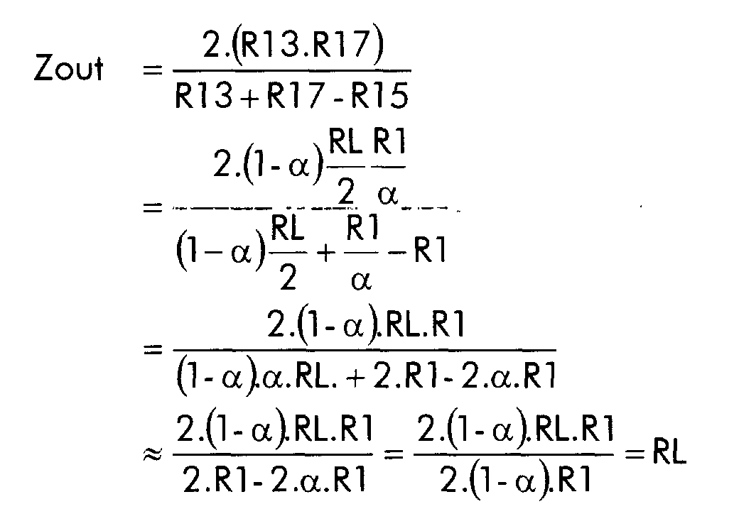
- This means indeed that the output impedance of the line driver is matched to the characteristic impedance of the transmission lines if the resistances are chosen as mentioned herein above.
- In order to obtain between the first and second output terminals OUT1, OUT2 a voltage of the required voltage level for driving the circuit connected to the transmission lines (e.g. 15 V), it can be seen that the amplifying device A can produce an output signal with a lower voltage level, if n is chosen larger than one. For example for obtaining an output voltage level of 15 V with a transformer with transformation ratio 1:5, the output voltage produced by the amplifying device does not need to exceed 3 V. Thus thanks to a high transformation ratio, a high line driver output voltage can be generated with a low power supply voltage for the operational amplifier. Therefore, the operational amplifier can be integrated on a chip using conventional techniques. The resistor values for active back termination become realisable with sufficient resolution. The active back termination resistive circuit is now located at the side of the transformer with most windings.
- While the invention has been shown and described with reference to a preferred embodiment, it will be understood by those skilled in the art that various changes or modifications in form and detail may be made without departing from the scope and spirit of this invention.
Claims (12)
- A broadband line driver comprising an amplifying device (A) with an input and an output, and a transforming device (T) coupled in series with the output of the amplifying device (A),
CHARACTERISED IN THAT the transforming device is located in a feedback loop that couples the output of the amplifying device (A) to the input of the amplifying device (A). - The broadband line driver according to claim 1,
CHARACTERISED IN THAT the transforming device (T) has a transformation ratio which is higher than 1:2. - The broadband line driver according to claim 1 or 2,
wherein a feedback circuit is connected between an output of the transforming device and the input of the amplifying device. - The broadband driver according to claim 3,
wherein the feedback circuit comprises resistors. - The broadband line driver according to any of the preceding claims, comprising:a first input terminal (IN1) and a second input terminal (IN2) as well as a first output terminal (OUT1) and a second output terminal (OUT2);the amplifying device (A) having a first and a second device input terminal (All, A12) and a first and a second device output terminal (AO1, A02),the transforming device comprising a transformer (T) with transformation ratio 1:n (n≥1) and comprising a primary winding with a first terminal (T11) and a second terminal (T12) and a secondary winding with a first terminal (T21) and a second terminal (T22), the first device output terminal (AO1) being coupled to a first terminal (T11) of the primary winding of the transformer (T), and the second device output terminal (AO2) being coupled to the second terminal (T12) of the primary winding, the first terminal (T21) of the secondary winding being coupled to the first output terminal (OUT1), and the second terminal (T22) being coupled to the second output terminal (OUT2),a first resistor (R17) being connected between the second output terminal (OUT2) and the first device input terminal (Al1), and a second resistor(R18) being coupled between the first output terminal (OUT1) and the second device input terminal (A12).
- The broadband driver according to claim 5,
wherein:the first device input terminal (All) is coupled to the first input terminal (IN1) over a third resistor (R11),the second device input terminal (A12) is coupled to the second input terminal (IN2) of the line driver over a fourth resistor (R12),a fifth resistor (R13) is connected between the first terminal (T12) of the secondary winding of the transformer (T) and the first output terminal (OUT1), and a sixth resistor (R14) is connected between the second terminal (T22) of the secondary winding of the transformer (T) and the second output terminal (OUT2),a seventh resistor (R15) is connected between the first terminal (T12) of the secondary winding of the transformer (T) and the first device input terminal (Al1) and a eighth resistor (R16) is connected between the second terminal (T22) of the secondary winding of the transformer (T) and the second device input terminal (A12). - The broadband line driver according to claim 6,
CHARACTERISED IN THAT the third resistor (R11) and the fourth resistor (R12) have substantially the same resistance value. - The broadband line driver according to any of claims 6 or 7,
CHARACTERISED IN THAT the fifth resistor (R13) and the sixth resistor (R14) have substantially the same resistance value. - The broadband line driver according to any of claims 6 to 8,
CHARACTERISED IN THAT the seventh resistor (R15) and the eighth resistor (R16) have substantially the same resistance value. - The broadband line driver according to any of claims 5 to 9,
CHARACTERISED IN THAT the first resistor (R17) and the second resistor (R18) have substantially the same resistance value. - Digital subscriber line analogue front end comprising a broadband line driver according to any of the previous claims.
- A method of operating a broadband line driver comprising an amplifying device, comprising the steps of:transforming the output voltage of the amplifying device to a higher value;feeding back a signal from the transformed output voltage to an input of the amplifying device.
Priority Applications (5)
| Application Number | Priority Date | Filing Date | Title |
|---|---|---|---|
| DE60026265T DE60026265T2 (en) | 2000-07-24 | 2000-07-24 | Low-voltage broadband line driver |
| AT00402123T ATE319252T1 (en) | 2000-07-24 | 2000-07-24 | BROADBAND LOW VOLTAGE LINE DRIVER |
| EP00402123A EP1176775B1 (en) | 2000-07-24 | 2000-07-24 | Low voltage broadband line driver |
| JP2001213273A JP2002100942A (en) | 2000-07-24 | 2001-07-13 | Low voltage broadband line driver |
| US09/910,037 US6985578B2 (en) | 2000-07-24 | 2001-07-23 | Low voltage broadband line driver |
Applications Claiming Priority (1)
| Application Number | Priority Date | Filing Date | Title |
|---|---|---|---|
| EP00402123A EP1176775B1 (en) | 2000-07-24 | 2000-07-24 | Low voltage broadband line driver |
Publications (2)
| Publication Number | Publication Date |
|---|---|
| EP1176775A1 true EP1176775A1 (en) | 2002-01-30 |
| EP1176775B1 EP1176775B1 (en) | 2006-03-01 |
Family
ID=8173783
Family Applications (1)
| Application Number | Title | Priority Date | Filing Date |
|---|---|---|---|
| EP00402123A Expired - Lifetime EP1176775B1 (en) | 2000-07-24 | 2000-07-24 | Low voltage broadband line driver |
Country Status (5)
| Country | Link |
|---|---|
| US (1) | US6985578B2 (en) |
| EP (1) | EP1176775B1 (en) |
| JP (1) | JP2002100942A (en) |
| AT (1) | ATE319252T1 (en) |
| DE (1) | DE60026265T2 (en) |
Families Citing this family (3)
| Publication number | Priority date | Publication date | Assignee | Title |
|---|---|---|---|---|
| ATE314769T1 (en) * | 2002-01-04 | 2006-01-15 | Cit Alcatel | IMPENDANCE ADJUSTMENT FOR LINE DRIVER |
| DE102005030049B4 (en) * | 2005-06-27 | 2007-09-13 | Infineon Technologies Ag | Driver circuit for a telephone line |
| WO2007063494A1 (en) | 2005-12-02 | 2007-06-07 | Nxp B.V. | Low noise amplifier |
Citations (2)
| Publication number | Priority date | Publication date | Assignee | Title |
|---|---|---|---|---|
| EP0901221A1 (en) * | 1997-09-05 | 1999-03-10 | Alcatel | Differential output amplifier arrangement and method for tuning the output impedance of a differential output amplifier |
| WO1999039433A1 (en) * | 1998-01-29 | 1999-08-05 | Telefonaktiebolaget Lm Ericsson (Publ) | Active impedance converter |
Family Cites Families (2)
| Publication number | Priority date | Publication date | Assignee | Title |
|---|---|---|---|---|
| US5038375A (en) * | 1989-06-23 | 1991-08-06 | Aptek Technologies, Inc. | Circuit arrangement for preventing gain from responding to frequency variation despite the presence of an isolation transformer |
| US6198818B1 (en) * | 1997-06-17 | 2001-03-06 | Paradyne Corporation | Method and apparatus for controlling the input impedance of an analog front end circuit of a data communications equipment (DCE) device |
-
2000
- 2000-07-24 AT AT00402123T patent/ATE319252T1/en not_active IP Right Cessation
- 2000-07-24 DE DE60026265T patent/DE60026265T2/en not_active Expired - Lifetime
- 2000-07-24 EP EP00402123A patent/EP1176775B1/en not_active Expired - Lifetime
-
2001
- 2001-07-13 JP JP2001213273A patent/JP2002100942A/en not_active Withdrawn
- 2001-07-23 US US09/910,037 patent/US6985578B2/en not_active Expired - Lifetime
Patent Citations (2)
| Publication number | Priority date | Publication date | Assignee | Title |
|---|---|---|---|---|
| EP0901221A1 (en) * | 1997-09-05 | 1999-03-10 | Alcatel | Differential output amplifier arrangement and method for tuning the output impedance of a differential output amplifier |
| WO1999039433A1 (en) * | 1998-01-29 | 1999-08-05 | Telefonaktiebolaget Lm Ericsson (Publ) | Active impedance converter |
Non-Patent Citations (4)
| Title |
|---|
| NASH E: "LINE-DRIVER DESIGN FOR BROADBAND COMMUNICATIONS APPLICATIONS", ELECTRONIC DESIGN,US,PENTON PUBLISHING, CLEVELAND, OH, vol. 45, no. 27, 1 December 1997 (1997-12-01), pages 81 - 82,84,86,88, XP000755760, ISSN: 0013-4872 * |
| NASH E: "SAVING DYNAMIC POWER IN HDSL LINE DRIVING APPLICATIONS", ELECTRONIC DESIGN,US,PENTON PUBLISHING, CLEVELAND, OH, vol. 45, no. 12, 9 June 1997 (1997-06-09), pages 88,90,92, XP000731500, ISSN: 0013-4872 * |
| SCWEBER B: "ANALOG FRONT ENDS BRIDG THE XDSL-TO-REAL-WORLD CHASM", EDN ELECTRICAL DESIGN NEWS,CAHNERS PUBLISHING CO. NEWTON, MASSACHUSETTS,US, vol. 44, no. 7, 1 April 1999 (1999-04-01), pages 48,50,52,54,56,58,60,62,64, XP000899059, ISSN: 0012-7515 * |
| STEFFES M ET AL: "OPTIMIZING PERFORMANCE IN AN XDSL LINE DRIVER", ELECTRONIC DESIGN,PENTON PUBLISHING, CLEVELAND, OH,US, vol. 47, no. 8, 19 April 1999 (1999-04-19), pages 44,46,48,52,54,56,58, XP000893613, ISSN: 0013-4872 * |
Also Published As
| Publication number | Publication date |
|---|---|
| EP1176775B1 (en) | 2006-03-01 |
| JP2002100942A (en) | 2002-04-05 |
| ATE319252T1 (en) | 2006-03-15 |
| US20020034294A1 (en) | 2002-03-21 |
| US6985578B2 (en) | 2006-01-10 |
| DE60026265D1 (en) | 2006-04-27 |
| DE60026265T2 (en) | 2006-11-23 |
Similar Documents
| Publication | Publication Date | Title |
|---|---|---|
| US5856758A (en) | Low distortion driver employing positive feedback for reducing power loss in output impedance that effectively matches the impedance of driven line | |
| US5822426A (en) | Balanced hybrid circuit | |
| CA2401539C (en) | Method and device for active impedance matching | |
| EP0026931A1 (en) | Transceiver for full duplex transmission of digital signals on a single line | |
| EP1391055B1 (en) | Line interface with a matching impedance coupled to a feedback path | |
| US7483528B2 (en) | Loop extender with selectable line termination and equalization | |
| EP1241799B1 (en) | Hybrid circuit for a broadband modem | |
| US8208462B2 (en) | Line driver for an adaptive hybrid circuit | |
| US6999743B2 (en) | Line interface with second order high pass transfer function | |
| US6452938B1 (en) | System and method to reduce electromagnetic interference emissions in a network interface | |
| EP1176775A1 (en) | Low voltage broadband line driver | |
| EP1612934B1 (en) | Class d-amplifier | |
| US6970515B1 (en) | Line driver for asymmetric digital subscriber line system | |
| US20060062378A1 (en) | Line interface with analog echo cancellation | |
| US6369650B1 (en) | Impedance synthesis and DC biasing method and architecture for DSL/cable line drivers | |
| US7349465B2 (en) | Line interface system | |
| US7020277B1 (en) | DSL line interface having low-pass filter characteristic with reduced external components | |
| US20040184558A1 (en) | Transmitter for transmitting digital data over a transmission line | |
| US20020098863A1 (en) | Broadband driver | |
| US20040232953A1 (en) | Line driver | |
| US20020024381A1 (en) | Power efficient line driver with 4X supply voltage swing and active termination | |
| EP1326390A1 (en) | Impedance matching in line drivers | |
| JP4668599B2 (en) | Wideband offset circuit | |
| US6252532B1 (en) | Programmable compensation and frequency equalization for network systems | |
| US20040095203A1 (en) | Transmission system |
Legal Events
| Date | Code | Title | Description |
|---|---|---|---|
| PUAI | Public reference made under article 153(3) epc to a published international application that has entered the european phase |
Free format text: ORIGINAL CODE: 0009012 |
|
| AK | Designated contracting states |
Kind code of ref document: A1 Designated state(s): AT BE CH CY DE DK ES FI FR GB GR IE IT LI LU MC NL PT SE |
|
| AX | Request for extension of the european patent |
Free format text: AL;LT;LV;MK;RO;SI |
|
| 17P | Request for examination filed |
Effective date: 20020730 |
|
| AKX | Designation fees paid |
Free format text: DE ES FR GB IT |
|
| RBV | Designated contracting states (corrected) |
Designated state(s): AT BE CH CY DE DK ES FI FR GB GR IE IT LI LU MC NL PT SE |
|
| 17Q | First examination report despatched |
Effective date: 20050512 |
|
| GRAP | Despatch of communication of intention to grant a patent |
Free format text: ORIGINAL CODE: EPIDOSNIGR1 |
|
| GRAS | Grant fee paid |
Free format text: ORIGINAL CODE: EPIDOSNIGR3 |
|
| GRAA | (expected) grant |
Free format text: ORIGINAL CODE: 0009210 |
|
| AK | Designated contracting states |
Kind code of ref document: B1 Designated state(s): AT BE CH CY DE DK ES FI FR GB GR IE IT LI LU MC NL PT SE |
|
| PG25 | Lapsed in a contracting state [announced via postgrant information from national office to epo] |
Ref country code: AT Free format text: LAPSE BECAUSE OF FAILURE TO SUBMIT A TRANSLATION OF THE DESCRIPTION OR TO PAY THE FEE WITHIN THE PRESCRIBED TIME-LIMIT Effective date: 20060301 Ref country code: NL Free format text: LAPSE BECAUSE OF FAILURE TO SUBMIT A TRANSLATION OF THE DESCRIPTION OR TO PAY THE FEE WITHIN THE PRESCRIBED TIME-LIMIT Effective date: 20060301 Ref country code: LI Free format text: LAPSE BECAUSE OF FAILURE TO SUBMIT A TRANSLATION OF THE DESCRIPTION OR TO PAY THE FEE WITHIN THE PRESCRIBED TIME-LIMIT Effective date: 20060301 Ref country code: FI Free format text: LAPSE BECAUSE OF FAILURE TO SUBMIT A TRANSLATION OF THE DESCRIPTION OR TO PAY THE FEE WITHIN THE PRESCRIBED TIME-LIMIT Effective date: 20060301 Ref country code: CH Free format text: LAPSE BECAUSE OF FAILURE TO SUBMIT A TRANSLATION OF THE DESCRIPTION OR TO PAY THE FEE WITHIN THE PRESCRIBED TIME-LIMIT Effective date: 20060301 Ref country code: BE Free format text: LAPSE BECAUSE OF FAILURE TO SUBMIT A TRANSLATION OF THE DESCRIPTION OR TO PAY THE FEE WITHIN THE PRESCRIBED TIME-LIMIT Effective date: 20060301 |
|
| REG | Reference to a national code |
Ref country code: GB Ref legal event code: FG4D |
|
| REG | Reference to a national code |
Ref country code: CH Ref legal event code: EP |
|
| REG | Reference to a national code |
Ref country code: IE Ref legal event code: FG4D |
|
| REF | Corresponds to: |
Ref document number: 60026265 Country of ref document: DE Date of ref document: 20060427 Kind code of ref document: P |
|
| PG25 | Lapsed in a contracting state [announced via postgrant information from national office to epo] |
Ref country code: SE Free format text: LAPSE BECAUSE OF FAILURE TO SUBMIT A TRANSLATION OF THE DESCRIPTION OR TO PAY THE FEE WITHIN THE PRESCRIBED TIME-LIMIT Effective date: 20060601 Ref country code: DK Free format text: LAPSE BECAUSE OF FAILURE TO SUBMIT A TRANSLATION OF THE DESCRIPTION OR TO PAY THE FEE WITHIN THE PRESCRIBED TIME-LIMIT Effective date: 20060601 |
|
| PG25 | Lapsed in a contracting state [announced via postgrant information from national office to epo] |
Ref country code: ES Free format text: LAPSE BECAUSE OF FAILURE TO SUBMIT A TRANSLATION OF THE DESCRIPTION OR TO PAY THE FEE WITHIN THE PRESCRIBED TIME-LIMIT Effective date: 20060612 |
|
| PG25 | Lapsed in a contracting state [announced via postgrant information from national office to epo] |
Ref country code: IE Free format text: LAPSE BECAUSE OF NON-PAYMENT OF DUE FEES Effective date: 20060724 |
|
| PG25 | Lapsed in a contracting state [announced via postgrant information from national office to epo] |
Ref country code: MC Free format text: LAPSE BECAUSE OF NON-PAYMENT OF DUE FEES Effective date: 20060731 |
|
| PG25 | Lapsed in a contracting state [announced via postgrant information from national office to epo] |
Ref country code: PT Free format text: LAPSE BECAUSE OF FAILURE TO SUBMIT A TRANSLATION OF THE DESCRIPTION OR TO PAY THE FEE WITHIN THE PRESCRIBED TIME-LIMIT Effective date: 20060801 |
|
| ET | Fr: translation filed | ||
| NLV1 | Nl: lapsed or annulled due to failure to fulfill the requirements of art. 29p and 29m of the patents act | ||
| REG | Reference to a national code |
Ref country code: CH Ref legal event code: PL |
|
| PLBE | No opposition filed within time limit |
Free format text: ORIGINAL CODE: 0009261 |
|
| STAA | Information on the status of an ep patent application or granted ep patent |
Free format text: STATUS: NO OPPOSITION FILED WITHIN TIME LIMIT |
|
| 26N | No opposition filed |
Effective date: 20061204 |
|
| PG25 | Lapsed in a contracting state [announced via postgrant information from national office to epo] |
Ref country code: GR Free format text: LAPSE BECAUSE OF FAILURE TO SUBMIT A TRANSLATION OF THE DESCRIPTION OR TO PAY THE FEE WITHIN THE PRESCRIBED TIME-LIMIT Effective date: 20060602 |
|
| PG25 | Lapsed in a contracting state [announced via postgrant information from national office to epo] |
Ref country code: LU Free format text: LAPSE BECAUSE OF NON-PAYMENT OF DUE FEES Effective date: 20060724 |
|
| PG25 | Lapsed in a contracting state [announced via postgrant information from national office to epo] |
Ref country code: CY Free format text: LAPSE BECAUSE OF FAILURE TO SUBMIT A TRANSLATION OF THE DESCRIPTION OR TO PAY THE FEE WITHIN THE PRESCRIBED TIME-LIMIT Effective date: 20060301 |
|
| REG | Reference to a national code |
Ref country code: FR Ref legal event code: GC Effective date: 20140717 |
|
| REG | Reference to a national code |
Ref country code: FR Ref legal event code: RG Effective date: 20141016 |
|
| REG | Reference to a national code |
Ref country code: FR Ref legal event code: PLFP Year of fee payment: 16 |
|
| REG | Reference to a national code |
Ref country code: FR Ref legal event code: PLFP Year of fee payment: 17 |
|
| PGFP | Annual fee paid to national office [announced via postgrant information from national office to epo] |
Ref country code: DE Payment date: 20160722 Year of fee payment: 17 Ref country code: IT Payment date: 20160725 Year of fee payment: 17 Ref country code: GB Payment date: 20160721 Year of fee payment: 17 |
|
| PGFP | Annual fee paid to national office [announced via postgrant information from national office to epo] |
Ref country code: FR Payment date: 20160721 Year of fee payment: 17 |
|
| REG | Reference to a national code |
Ref country code: DE Ref legal event code: R119 Ref document number: 60026265 Country of ref document: DE |
|
| GBPC | Gb: european patent ceased through non-payment of renewal fee |
Effective date: 20170724 |
|
| REG | Reference to a national code |
Ref country code: FR Ref legal event code: ST Effective date: 20180330 |
|
| PG25 | Lapsed in a contracting state [announced via postgrant information from national office to epo] |
Ref country code: DE Free format text: LAPSE BECAUSE OF NON-PAYMENT OF DUE FEES Effective date: 20180201 Ref country code: GB Free format text: LAPSE BECAUSE OF NON-PAYMENT OF DUE FEES Effective date: 20170724 |
|
| PG25 | Lapsed in a contracting state [announced via postgrant information from national office to epo] |
Ref country code: FR Free format text: LAPSE BECAUSE OF NON-PAYMENT OF DUE FEES Effective date: 20170731 |
|
| PG25 | Lapsed in a contracting state [announced via postgrant information from national office to epo] |
Ref country code: IT Free format text: LAPSE BECAUSE OF NON-PAYMENT OF DUE FEES Effective date: 20170724 |
|
| REG | Reference to a national code |
Ref country code: DE Ref legal event code: R081 Ref document number: 60026265 Country of ref document: DE Owner name: WSOU INVESTMENTS, LLC, LOS ANGELES, US Free format text: FORMER OWNER: ALCATEL LUCENT, PARIS, FR Ref country code: DE Ref legal event code: R082 Ref document number: 60026265 Country of ref document: DE Representative=s name: BARKHOFF REIMANN VOSSIUS, DE |
|
| REG | Reference to a national code |
Ref country code: GB Ref legal event code: 732E Free format text: REGISTERED BETWEEN 20200820 AND 20200826 |