EP1176705A1 - Low consumption converter directly connectable to the mains and the method for driving it - Google Patents
Low consumption converter directly connectable to the mains and the method for driving it Download PDFInfo
- Publication number
- EP1176705A1 EP1176705A1 EP00830540A EP00830540A EP1176705A1 EP 1176705 A1 EP1176705 A1 EP 1176705A1 EP 00830540 A EP00830540 A EP 00830540A EP 00830540 A EP00830540 A EP 00830540A EP 1176705 A1 EP1176705 A1 EP 1176705A1
- Authority
- EP
- European Patent Office
- Prior art keywords
- voltage
- signal
- converter
- load
- producing
- Prior art date
- Legal status (The legal status is an assumption and is not a legal conclusion. Google has not performed a legal analysis and makes no representation as to the accuracy of the status listed.)
- Granted
Links
Images
Classifications
-
- H—ELECTRICITY
- H02—GENERATION; CONVERSION OR DISTRIBUTION OF ELECTRIC POWER
- H02M—APPARATUS FOR CONVERSION BETWEEN AC AND AC, BETWEEN AC AND DC, OR BETWEEN DC AND DC, AND FOR USE WITH MAINS OR SIMILAR POWER SUPPLY SYSTEMS; CONVERSION OF DC OR AC INPUT POWER INTO SURGE OUTPUT POWER; CONTROL OR REGULATION THEREOF
- H02M1/00—Details of apparatus for conversion
- H02M1/42—Circuits or arrangements for compensating for or adjusting power factor in converters or inverters
- H02M1/4208—Arrangements for improving power factor of AC input
- H02M1/4225—Arrangements for improving power factor of AC input using a non-isolated boost converter
-
- H—ELECTRICITY
- H02—GENERATION; CONVERSION OR DISTRIBUTION OF ELECTRIC POWER
- H02J—ELECTRIC POWER NETWORKS; CIRCUIT ARRANGEMENTS OR SYSTEMS FOR SUPPLYING OR DISTRIBUTING ELECTRIC POWER; SYSTEMS FOR STORING ELECTRIC ENERGY
- H02J9/00—Circuit arrangements for emergency or stand-by power supply, e.g. for emergency lighting
- H02J9/005—Circuit arrangements for emergency or stand-by power supply, e.g. for emergency lighting using a power saving mode
- H02J9/007—Detection of the absence of a load
-
- H—ELECTRICITY
- H02—GENERATION; CONVERSION OR DISTRIBUTION OF ELECTRIC POWER
- H02M—APPARATUS FOR CONVERSION BETWEEN AC AND AC, BETWEEN AC AND DC, OR BETWEEN DC AND DC, AND FOR USE WITH MAINS OR SIMILAR POWER SUPPLY SYSTEMS; CONVERSION OF DC OR AC INPUT POWER INTO SURGE OUTPUT POWER; CONTROL OR REGULATION THEREOF
- H02M1/00—Details of apparatus for conversion
- H02M1/0003—Details of control, feedback or regulation circuits
- H02M1/0032—Control circuits allowing low power mode operation, e.g. in standby mode
-
- H—ELECTRICITY
- H02—GENERATION; CONVERSION OR DISTRIBUTION OF ELECTRIC POWER
- H02M—APPARATUS FOR CONVERSION BETWEEN AC AND AC, BETWEEN AC AND DC, OR BETWEEN DC AND DC, AND FOR USE WITH MAINS OR SIMILAR POWER SUPPLY SYSTEMS; CONVERSION OF DC OR AC INPUT POWER INTO SURGE OUTPUT POWER; CONTROL OR REGULATION THEREOF
- H02M1/00—Details of apparatus for conversion
- H02M1/0067—Converter structures employing plural converter units, other than for parallel operation of the units on a single load
- H02M1/007—Plural converter units in cascade
-
- Y—GENERAL TAGGING OF NEW TECHNOLOGICAL DEVELOPMENTS; GENERAL TAGGING OF CROSS-SECTIONAL TECHNOLOGIES SPANNING OVER SEVERAL SECTIONS OF THE IPC; TECHNICAL SUBJECTS COVERED BY FORMER USPC CROSS-REFERENCE ART COLLECTIONS [XRACs] AND DIGESTS
- Y02—TECHNOLOGIES OR APPLICATIONS FOR MITIGATION OR ADAPTATION AGAINST CLIMATE CHANGE
- Y02B—CLIMATE CHANGE MITIGATION TECHNOLOGIES RELATED TO BUILDINGS, e.g. HOUSING, HOUSE APPLIANCES OR RELATED END-USER APPLICATIONS
- Y02B70/00—Technologies for an efficient end-user side electric power management and consumption
- Y02B70/10—Technologies improving the efficiency by using switched-mode power supplies [SMPS], i.e. efficient power electronics conversion e.g. power factor correction or reduction of losses in power supplies or efficient standby modes
-
- Y—GENERAL TAGGING OF NEW TECHNOLOGICAL DEVELOPMENTS; GENERAL TAGGING OF CROSS-SECTIONAL TECHNOLOGIES SPANNING OVER SEVERAL SECTIONS OF THE IPC; TECHNICAL SUBJECTS COVERED BY FORMER USPC CROSS-REFERENCE ART COLLECTIONS [XRACs] AND DIGESTS
- Y02—TECHNOLOGIES OR APPLICATIONS FOR MITIGATION OR ADAPTATION AGAINST CLIMATE CHANGE
- Y02B—CLIMATE CHANGE MITIGATION TECHNOLOGIES RELATED TO BUILDINGS, e.g. HOUSING, HOUSE APPLIANCES OR RELATED END-USER APPLICATIONS
- Y02B70/00—Technologies for an efficient end-user side electric power management and consumption
- Y02B70/30—Systems integrating technologies related to power network operation and communication or information technologies for improving the carbon footprint of the management of residential or tertiary loads, i.e. smart grids as climate change mitigation technology in the buildings sector, including also the last stages of power distribution and the control, monitoring or operating management systems at local level
-
- Y—GENERAL TAGGING OF NEW TECHNOLOGICAL DEVELOPMENTS; GENERAL TAGGING OF CROSS-SECTIONAL TECHNOLOGIES SPANNING OVER SEVERAL SECTIONS OF THE IPC; TECHNICAL SUBJECTS COVERED BY FORMER USPC CROSS-REFERENCE ART COLLECTIONS [XRACs] AND DIGESTS
- Y02—TECHNOLOGIES OR APPLICATIONS FOR MITIGATION OR ADAPTATION AGAINST CLIMATE CHANGE
- Y02P—CLIMATE CHANGE MITIGATION TECHNOLOGIES IN THE PRODUCTION OR PROCESSING OF GOODS
- Y02P80/00—Climate change mitigation technologies for sector-wide applications
- Y02P80/10—Efficient use of energy, e.g. using compressed air or pressurized fluid as energy carrier
-
- Y—GENERAL TAGGING OF NEW TECHNOLOGICAL DEVELOPMENTS; GENERAL TAGGING OF CROSS-SECTIONAL TECHNOLOGIES SPANNING OVER SEVERAL SECTIONS OF THE IPC; TECHNICAL SUBJECTS COVERED BY FORMER USPC CROSS-REFERENCE ART COLLECTIONS [XRACs] AND DIGESTS
- Y04—INFORMATION OR COMMUNICATION TECHNOLOGIES HAVING AN IMPACT ON OTHER TECHNOLOGY AREAS
- Y04S—SYSTEMS INTEGRATING TECHNOLOGIES RELATED TO POWER NETWORK OPERATION, COMMUNICATION OR INFORMATION TECHNOLOGIES FOR IMPROVING THE ELECTRICAL POWER GENERATION, TRANSMISSION, DISTRIBUTION, MANAGEMENT OR USAGE, i.e. SMART GRIDS
- Y04S20/00—Management or operation of end-user stationary applications or the last stages of power distribution; Controlling, monitoring or operating thereof
- Y04S20/20—End-user application control systems
Definitions
- the invention relates in general to converters, adapters, battery chargers and similar circuits, and more specifically to a method of driving a low consumption converter directly connectable to the mains.
- Power supplies are generally constituted by a DC-DC converter coupled to the mains through one or several stages.
- a square wave drives the control terminal of a power switch determining its conductive or not conductive state.
- the output voltage is increased by increasing the duration of the phase of conduction of the switch, and decreased by increasing the duration of the phase of no conduction; thus the output voltage is controlled by varying the duty cycle of the driving square wave.
- the power switch is a MOS transistor
- a non negligible amount of power is spent to charge periodically the gate of the switching transistor.
- Power dissipation increases with the increase of the switching frequency in a measure that sensibly affects the overall efficiency of the converter.
- such a power dissipation lowers the efficiency of the converter especially when the load is relatively small. For this reason, present day devices implement a lowering of the switching frequency when supplying a relatively small load.
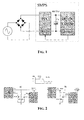
- a two stage converter may be constituted by, as illustrated in Fig. 1, a rectifier coupled to the mains, a power factor pre-regulating circuit PFC (Power Factor Corrector) supplied with the rectified mains voltage and producing a DC voltage of a certain nominal value and a DC-DC converter, input with the DC voltage of nominal value, controlling a load.
- the DC-DC converter may be based on a control scheme of any suitable kind (PWM, quasi resonant, resonant, etc.).
- a well known solution to reduce energy consumption under relatively small or null load conditions consists in reducing the switching frequency of the switches of the PFC stage or of the DC-DC stages, separately.
- an object of the present invention is a converter, directly connectable to the mains, comprising a rectifier of the network voltage, a pre-regulating circuit, supplied with the rectified network voltage and producing a DC voltage of a certain nominal value, a DC-DC converter that is input with the nominal DC voltage and produces a pre-established DC voltage on an output node, and a sensing circuit that produces a signal representative of the load currently supplied by the converter for eventually disabling said pre-regulating circuit.
- An essential feature is the presence of a control circuit receiving as an input the signal representative of the current load level and generating a disabling signal for as long as the load does not exceeds a pre-established value.
- a converter provided with the above mentioned control circuit can be driven according to a method that comprises the steps of sensing the level of load currently being supplied, comparing the sensed load with a pre-established threshold and generating the above mentioned disabling signal as long as the load remains lower than said pre-established threshold.
- a preferred embodiment of the converter of the invention includes a pre-regulating circuit comprising a power factor correction circuit that is supplied with the rectified network voltage and receives at an input a signal representative of the nominal DC voltage and producing a correction signal, a power driver supplied with the rectified network voltage and receiving at an input a driving signal and the correction signal and producing said nominal DC voltage if the driving voltage is disabled and a drive control circuit producing the driving signal if the voltage on an input node thereof is null.
- the drive control circuit can be simply realized by functionally coupling a comparator, that produces the disabling signal if the signal representative of the load surpasses a pre-established threshold, to a switch, driven by the disabling signal, that electrically isolates or connects to a reference voltage the input node of the driving circuit.
- the converter of the invention shows an enhanced performance in terms of energy saving than comparable known converters, because when the DC-DC converter detects a relatively large load, the PFC pre-regulating circuit is automatically set to a low consumption (quiescent) condition. On the contrary when the load increases, the PFC resumes its normal functioning, outputting the required power and voltage.
- the voltage on the bulk capacitor Co that couples the PFC to the converter is reduced from the value of the regulated voltage to the much lower rectified and filtered network voltage.
- I leak ⁇ 0.02 * C( ⁇ F)* V R (V) + 15 ⁇ A the turning off of the PFC results in a reduction of the self-consumption of the capacitor, and thus in a further energy saving.
- the reduction of the voltage onto the capacitor Co thus reducing the voltage supplied to the converter, allows a reduction of the switching losses of the converter and of the PFC, caused by parasitic elements.
- the driving method of the invention substantially consists in detecting the level of load being supplied, disabling the PFC pre-regulating circuit each time the load drops below a certain pre-established threshold and enabling the PFC preregulating circuit functioning when the load reaches and/or exceeds the threshold.
- a converter of the invention can be realized with a common DC-DC converter by detecting the load level, providing a signal representative of the current load condition to a stand-by control circuit that drives an on/off circuit controlling the functioning of the PFC pre-regulating stage of the converter.
- the disabling on/off signal input to the PFC stage of the converter can be generated within the DC-DC converter itself or by any external circuit detecting the power being delivered to the load.
- Fig. 2 Two possible embodiments of the invention conveniently using commercially available PFC pre-regulating circuit and DC-DC converter, respectively the devices L6561 and L5991 of STMicroelectronics, are shown in Fig. 2.
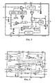
- the block diagrams of the two commercial devices are depicted in Fig. 3 and Fig. 4, respectively.
- the device L6561 is essentially constituted by a voltage regulator VOLTAGE_REGULATOR supplied with the rectified network voltage Vcc and receiving at its input INV a signal representative of the nominal DC voltage produced by the pre-regulator, by a power driver DRIVER supplied with the voltage VCC and driven by a driving circuit DISABLE, disabling the driver if the voltage on the node ZCD is null.
- the transistor 1.a is coupled to the zener diode and acts as a comparator producing, on the base of transistor 1.b, a null collector-emitter voltage if the voltage on the node ST-BY is equal to or greater than 5V, or a voltage suitable to set in conduction state the transistor 1.b if on ST-BY a voltage lower than 5V is present. Such a collector-emitter voltage represents the disabling signal.
- the transistor 1.b is a switch driven by the disabling signal that connects or disconnects to ground the node ZCD of the L6561 device.
- An alternative way of turning off the device L6561 may be that of disconnecting it from the supply line in the way shown in Fig. 2b.
- the switch driven by the disabling signal couples the device L6561 to the VCC line.
- the commercial device L5991 whose block diagram is depicted in Fig. 4, is provided with a logic circuit regulating the PWM driving signal that receives on the input node ISEN a signal representing the current delivered to the load, on the node SC a duty-cycle regulation signal and on the node RCT a clock signal.
- the device L5991 is also provided with a driver to the output nodes OUT and PGND of which is coupled the output bridge circuit, and with a stand-by circuit STAND-BY producing a selection signal on the node ST-BY, in order to reduce the frequency of the external oscillator that generates the clock signal to a minimum value whenever the load drops below a certain pre-established threshold.
- Such a stand-by circuit is commonly present in several other commercially available converters, for reducing the switching losses when the load is relatively low.
- the improved converter of the invention can be simply realized by inputting to any of the control circuits of Fig. 2 the selection signal that is already generated within these commercially available converters as a signal representative of the level of load.
Landscapes
- Engineering & Computer Science (AREA)
- Power Engineering (AREA)
- Dc-Dc Converters (AREA)
- Rectifiers (AREA)
Abstract
Description
Claims (5)
- A converter directly connectable to the mains comprising a rectifier stage of the network voltage, a power factor correction pre-regulating circuit supplied with the rectified network voltage and producing a DC voltage of a certain nominal value, a DC-DC converter supplied with said DC voltage of a certain nominal value and producing a pre-established DC voltage on an output node, sensing means producing a signal representative of the current level of load being supplied by the converter, characterized in that it comprisesa control circuit input with said signal representative of the level of load and generating a disabling signal of said power factor corrector pre-regulating circuit as long as the level of load does not exceed a certain pre-established threshold.
- The converter of claim 1, wherein said power factor correction pre-regulating circuit comprisescharacterized in that it further comprisesa correction circuit that receives at an input a signal representing the desired nominal DC voltage and produces a correction signal,a power driver supplied with the rectified network voltage and receiving as input a drive signal and said correction signal, producing said nominal DC voltage if said drive signal is disabled,a drive circuit producing said drive signal if the voltage on an input node thereof is null,a comparator producing the disabling signal if the signal representative of the level of load exceeds said pre-established threshold;a switch driven by said disabling signal that electrically isolates or connects to a reference voltage said input node of the drive control circuit.
- The converter according to claim 1 wherein said control circuit comprisesa comparator producing said disabling signal if the signal representative of the load exceeds a certain threshold;a switch driven by said disabling signal electrically connecting or disconnecting said power factor correction pre-regulating circuit to the output of said rectifier stage.
- The converter according to a claim from 1 to 3, wherein said DC-DC converter uses a clock whose frequency can be regulated between at least two distinct values by a selection circuit, a stand-by circuit (STAND-BY) producing said selection signal in function of the current delivered to the load, characterized in thatsaid signal representative of the level of load is activated when said selection signal assumes a value corresponding to the minimum frequency of the oscillator that generates said clock.
- A method of driving a converter directly connectable to the mains comprising a rectifier stage of the network voltage, a power factor correction pre-regulating circuit that may be disabled by a disabling signal fed with the rectified network voltage and producing a DC voltage equal to a certain nominal value, a DC-DC converter supplied with said nominal DC voltage and producing a certain DC voltage on an output node, comprising the steps ofsensing the level of load currently being supplied by the converter;comparing the sensed level of load with a pre-established threshold;producing said disabling signal as long as the level of load is lower than said pre-established threshold.
Priority Applications (3)
| Application Number | Priority Date | Filing Date | Title |
|---|---|---|---|
| EP00830540A EP1176705B1 (en) | 2000-07-28 | 2000-07-28 | Low consumption converter directly connectable to the mains |
| DE60003809T DE60003809T2 (en) | 2000-07-28 | 2000-07-28 | Low-consumption converter that can be connected directly to the network |
| US09/916,185 US6424549B1 (en) | 2000-07-28 | 2001-07-26 | Low consumption converter directly connectable to the mains |
Applications Claiming Priority (1)
| Application Number | Priority Date | Filing Date | Title |
|---|---|---|---|
| EP00830540A EP1176705B1 (en) | 2000-07-28 | 2000-07-28 | Low consumption converter directly connectable to the mains |
Publications (2)
| Publication Number | Publication Date |
|---|---|
| EP1176705A1 true EP1176705A1 (en) | 2002-01-30 |
| EP1176705B1 EP1176705B1 (en) | 2003-07-09 |
Family
ID=8175425
Family Applications (1)
| Application Number | Title | Priority Date | Filing Date |
|---|---|---|---|
| EP00830540A Expired - Lifetime EP1176705B1 (en) | 2000-07-28 | 2000-07-28 | Low consumption converter directly connectable to the mains |
Country Status (3)
| Country | Link |
|---|---|
| US (1) | US6424549B1 (en) |
| EP (1) | EP1176705B1 (en) |
| DE (1) | DE60003809T2 (en) |
Cited By (2)
| Publication number | Priority date | Publication date | Assignee | Title |
|---|---|---|---|---|
| EP2566024A1 (en) * | 2011-09-01 | 2013-03-06 | Nxp B.V. | An AC/DC converter having a switchable pfc, a controller therefor, and a method of operating a controller |
| GB2540570A (en) * | 2015-07-21 | 2017-01-25 | Dyson Technology Ltd | Battery charger |
Families Citing this family (10)
| Publication number | Priority date | Publication date | Assignee | Title |
|---|---|---|---|---|
| US7548441B2 (en) | 2004-02-24 | 2009-06-16 | Vlt, Inc. | Universal AC adapter |
| US7408795B2 (en) * | 2004-02-24 | 2008-08-05 | Vlt, Inc. | Energy storage and hold-up method and apparatus for high density power conversion |
| US7561446B1 (en) | 2005-09-15 | 2009-07-14 | Vlt, Inc. | Double-clamped ZVS buck-boost power converter |
| US20070139984A1 (en) * | 2005-12-20 | 2007-06-21 | Yu-Kang Lo | Resonant conversion control method and device with a very low standby power consumption |
| US20070174258A1 (en) * | 2006-01-23 | 2007-07-26 | Jones Scott A | Targeted mobile device advertisements |
| US8065286B2 (en) * | 2006-01-23 | 2011-11-22 | Chacha Search, Inc. | Scalable search system using human searchers |
| US7917788B2 (en) * | 2006-11-01 | 2011-03-29 | Freescale Semiconductor, Inc. | SOC with low power and performance modes |
| KR20100134650A (en) * | 2008-03-10 | 2010-12-23 | 테크티움 엘티디. | Green power supply for converting alternating current into regulated direct current output |
| CN101604904B (en) * | 2008-06-11 | 2011-07-13 | 康舒科技股份有限公司 | Switching Mode Power Supply Improves Light Load Efficiency |
| US8971075B2 (en) * | 2011-02-07 | 2015-03-03 | Texas Instruments Incorporated | Method and apparatus for generating an adaptive switching frequency for operating power factor correction circuit |
Citations (7)
| Publication number | Priority date | Publication date | Assignee | Title |
|---|---|---|---|---|
| US5600549A (en) * | 1994-09-20 | 1997-02-04 | Astec International, Ltd. | Power factor corrected electrical power converter |
| US5726871A (en) * | 1996-01-15 | 1998-03-10 | Lg Electronics Inc. | Power supply circuit with power saving mode for video display appliance |
| US5757166A (en) * | 1995-11-30 | 1998-05-26 | Motorola, Inc. | Power factor correction controlled boost converter with an improved zero current detection circuit for operation under high input voltage conditions |
| US5903138A (en) * | 1995-03-30 | 1999-05-11 | Micro Linear Corporation | Two-stage switching regulator having low power modes responsive to load power consumption |
| DE19805373A1 (en) * | 1998-02-11 | 1999-08-12 | Hahn Uwe | Circuit for mains stage for a primary clocked ac/dc mains stage, pref. for a TV receiver |
| US5960207A (en) * | 1997-01-21 | 1999-09-28 | Dell Usa, L.P. | System and method for reducing power losses by gating an active power factor conversion process |
| US6043633A (en) * | 1998-06-05 | 2000-03-28 | Systel Development & Industries | Power factor correction method and apparatus |
Family Cites Families (3)
| Publication number | Priority date | Publication date | Assignee | Title |
|---|---|---|---|---|
| US5790389A (en) * | 1996-05-31 | 1998-08-04 | Virginia Power Technologies, Inc. | Consolidated soft-switching AC/DC converters |
| US6023037A (en) * | 1998-11-05 | 2000-02-08 | Lincoln Global, Inc. | Electric ARC welder and plasma cutter |
| TW431059B (en) * | 1999-01-04 | 2001-04-21 | Skynet Electronic Co Ltd | Power factor correction circuit |
-
2000
- 2000-07-28 EP EP00830540A patent/EP1176705B1/en not_active Expired - Lifetime
- 2000-07-28 DE DE60003809T patent/DE60003809T2/en not_active Expired - Lifetime
-
2001
- 2001-07-26 US US09/916,185 patent/US6424549B1/en not_active Expired - Lifetime
Patent Citations (7)
| Publication number | Priority date | Publication date | Assignee | Title |
|---|---|---|---|---|
| US5600549A (en) * | 1994-09-20 | 1997-02-04 | Astec International, Ltd. | Power factor corrected electrical power converter |
| US5903138A (en) * | 1995-03-30 | 1999-05-11 | Micro Linear Corporation | Two-stage switching regulator having low power modes responsive to load power consumption |
| US5757166A (en) * | 1995-11-30 | 1998-05-26 | Motorola, Inc. | Power factor correction controlled boost converter with an improved zero current detection circuit for operation under high input voltage conditions |
| US5726871A (en) * | 1996-01-15 | 1998-03-10 | Lg Electronics Inc. | Power supply circuit with power saving mode for video display appliance |
| US5960207A (en) * | 1997-01-21 | 1999-09-28 | Dell Usa, L.P. | System and method for reducing power losses by gating an active power factor conversion process |
| DE19805373A1 (en) * | 1998-02-11 | 1999-08-12 | Hahn Uwe | Circuit for mains stage for a primary clocked ac/dc mains stage, pref. for a TV receiver |
| US6043633A (en) * | 1998-06-05 | 2000-03-28 | Systel Development & Industries | Power factor correction method and apparatus |
Cited By (7)
| Publication number | Priority date | Publication date | Assignee | Title |
|---|---|---|---|---|
| EP2566024A1 (en) * | 2011-09-01 | 2013-03-06 | Nxp B.V. | An AC/DC converter having a switchable pfc, a controller therefor, and a method of operating a controller |
| CN102969909A (en) * | 2011-09-01 | 2013-03-13 | Nxp股份有限公司 | An ac/dc converter having a switchable pfc, a controller therefor, and a method of operating a controller |
| US8963451B2 (en) | 2011-09-01 | 2015-02-24 | Nxp B.V. | AC/DC converter having a switchable PFC, a controller therfor, and a method of operating a contoller |
| CN102969909B (en) * | 2011-09-01 | 2016-04-13 | Nxp股份有限公司 | Having can the AC/DC transducer of switch P FC and the method for controller and operation control thereof |
| GB2540570A (en) * | 2015-07-21 | 2017-01-25 | Dyson Technology Ltd | Battery charger |
| CN107852007A (en) * | 2015-07-21 | 2018-03-27 | 戴森技术有限公司 | Battery charger |
| GB2540570B (en) * | 2015-07-21 | 2019-04-03 | Dyson Technology Ltd | Battery charger |
Also Published As
| Publication number | Publication date |
|---|---|
| US20020021576A1 (en) | 2002-02-21 |
| EP1176705B1 (en) | 2003-07-09 |
| DE60003809D1 (en) | 2003-08-14 |
| DE60003809T2 (en) | 2004-06-03 |
| US6424549B1 (en) | 2002-07-23 |
Similar Documents
| Publication | Publication Date | Title |
|---|---|---|
| US6903536B2 (en) | PFC-PWM controller having interleaved switching | |
| US6960906B2 (en) | Switching power supply | |
| US7852640B2 (en) | System and method for providing control for switch-mode power supply | |
| US9048742B2 (en) | Systems and methods for adjusting current consumption of control chips to reduce standby power consumption of power converters | |
| US9590513B2 (en) | Methods for operating a converter | |
| US5179508A (en) | Standby boost converter | |
| US5903138A (en) | Two-stage switching regulator having low power modes responsive to load power consumption | |
| US7208985B2 (en) | Semiconductor device for controlling switching power supply | |
| US7567065B2 (en) | Switching regulator and method for changing output voltages thereof | |
| US20010020802A1 (en) | Power unit | |
| US7012818B2 (en) | Switching power supply device | |
| US20040037098A1 (en) | Switching power supply | |
| US20040174149A1 (en) | Power supplying methods and apparatus that provide stable output voltage | |
| US20080049452A1 (en) | Ultralow Power stan-By Supply | |
| US20040145924A1 (en) | Pulse width modulation signal generator and switching mode power supply including the same | |
| EP1176705B1 (en) | Low consumption converter directly connectable to the mains | |
| US9343981B2 (en) | Charging device for charging a battery pack | |
| US8503195B1 (en) | System and method for zero volt switching of half bridge converters during startup and short circuit conditions | |
| JP3475904B2 (en) | Switching power supply | |
| US20230010170A1 (en) | Method of standby power supply | |
| JPH11341397A (en) | Remote control standby power supply | |
| US6233164B1 (en) | Protection circuit for a switched-mode power supply | |
| JP2006148988A (en) | Switching power supply circuit | |
| CN116365828A (en) | Power supply circuit of flyback converter, power supply method and flyback converter | |
| KR19980066100U (en) | Initial drive circuit of the monitor |
Legal Events
| Date | Code | Title | Description |
|---|---|---|---|
| PUAI | Public reference made under article 153(3) epc to a published international application that has entered the european phase |
Free format text: ORIGINAL CODE: 0009012 |
|
| AK | Designated contracting states |
Kind code of ref document: A1 Designated state(s): DE FR GB IT Kind code of ref document: A1 Designated state(s): AT BE CH CY DE DK ES FI FR GB GR IE IT LI LU MC NL PT SE |
|
| AX | Request for extension of the european patent |
Free format text: AL;LT;LV;MK;RO;SI |
|
| 17P | Request for examination filed |
Effective date: 20020507 |
|
| 17Q | First examination report despatched |
Effective date: 20020814 |
|
| AKX | Designation fees paid |
Free format text: DE FR GB IT |
|
| GRAH | Despatch of communication of intention to grant a patent |
Free format text: ORIGINAL CODE: EPIDOS IGRA |
|
| RTI1 | Title (correction) |
Free format text: LOW CONSUMPTION CONVERTER DIRECTLY CONNECTABLE TO THE MAINS |
|
| GRAH | Despatch of communication of intention to grant a patent |
Free format text: ORIGINAL CODE: EPIDOS IGRA |
|
| GRAA | (expected) grant |
Free format text: ORIGINAL CODE: 0009210 |
|
| AK | Designated contracting states |
Designated state(s): DE FR GB IT |
|
| REG | Reference to a national code |
Ref country code: GB Ref legal event code: FG4D |
|
| REF | Corresponds to: |
Ref document number: 60003809 Country of ref document: DE Date of ref document: 20030814 Kind code of ref document: P |
|
| REG | Reference to a national code |
Ref country code: IE Ref legal event code: FG4D |
|
| PLBE | No opposition filed within time limit |
Free format text: ORIGINAL CODE: 0009261 |
|
| STAA | Information on the status of an ep patent application or granted ep patent |
Free format text: STATUS: NO OPPOSITION FILED WITHIN TIME LIMIT |
|
| ET | Fr: translation filed | ||
| 26N | No opposition filed |
Effective date: 20040414 |
|
| PGFP | Annual fee paid to national office [announced via postgrant information from national office to epo] |
Ref country code: IT Payment date: 20070725 Year of fee payment: 8 |
|
| PGFP | Annual fee paid to national office [announced via postgrant information from national office to epo] |
Ref country code: FR Payment date: 20070730 Year of fee payment: 8 |
|
| REG | Reference to a national code |
Ref country code: FR Ref legal event code: ST Effective date: 20090331 |
|
| PG25 | Lapsed in a contracting state [announced via postgrant information from national office to epo] |
Ref country code: FR Free format text: LAPSE BECAUSE OF NON-PAYMENT OF DUE FEES Effective date: 20080731 Ref country code: IT Free format text: LAPSE BECAUSE OF NON-PAYMENT OF DUE FEES Effective date: 20080728 |
|
| PGFP | Annual fee paid to national office [announced via postgrant information from national office to epo] |
Ref country code: DE Payment date: 20100706 Year of fee payment: 11 Ref country code: GB Payment date: 20100628 Year of fee payment: 11 |
|
| GBPC | Gb: european patent ceased through non-payment of renewal fee |
Effective date: 20110728 |
|
| REG | Reference to a national code |
Ref country code: DE Ref legal event code: R231 Ref document number: 60003809 Country of ref document: DE |
|
| REG | Reference to a national code |
Ref country code: DE Ref legal event code: R119 Ref document number: 60003809 Country of ref document: DE Effective date: 20120201 |
|
| PG25 | Lapsed in a contracting state [announced via postgrant information from national office to epo] |
Ref country code: GB Free format text: LAPSE BECAUSE OF NON-PAYMENT OF DUE FEES Effective date: 20110728 |
|
| PG25 | Lapsed in a contracting state [announced via postgrant information from national office to epo] |
Ref country code: DE Free format text: LAPSE BECAUSE OF THE APPLICANT RENOUNCES Effective date: 20120417 |
|
| PG25 | Lapsed in a contracting state [announced via postgrant information from national office to epo] |
Ref country code: DE Free format text: LAPSE BECAUSE OF THE APPLICANT RENOUNCES Effective date: 20120201 |