EP1176643A2 - MOS power semiconductor device having a trench gate and method of making the same - Google Patents
MOS power semiconductor device having a trench gate and method of making the same Download PDFInfo
- Publication number
- EP1176643A2 EP1176643A2 EP01116709A EP01116709A EP1176643A2 EP 1176643 A2 EP1176643 A2 EP 1176643A2 EP 01116709 A EP01116709 A EP 01116709A EP 01116709 A EP01116709 A EP 01116709A EP 1176643 A2 EP1176643 A2 EP 1176643A2
- Authority
- EP
- European Patent Office
- Prior art keywords
- upper layer
- source regions
- trench
- power device
- conductance type
- Prior art date
- Legal status (The legal status is an assumption and is not a legal conclusion. Google has not performed a legal analysis and makes no representation as to the accuracy of the status listed.)
- Withdrawn
Links
Images

Classifications
-
- H—ELECTRICITY
- H10—SEMICONDUCTOR DEVICES; ELECTRIC SOLID-STATE DEVICES NOT OTHERWISE PROVIDED FOR
- H10D—INORGANIC ELECTRIC SEMICONDUCTOR DEVICES
- H10D30/00—Field-effect transistors [FET]
- H10D30/60—Insulated-gate field-effect transistors [IGFET]
- H10D30/64—Double-diffused metal-oxide semiconductor [DMOS] FETs
- H10D30/66—Vertical DMOS [VDMOS] FETs
-
- H—ELECTRICITY
- H10—SEMICONDUCTOR DEVICES; ELECTRIC SOLID-STATE DEVICES NOT OTHERWISE PROVIDED FOR
- H10D—INORGANIC ELECTRIC SEMICONDUCTOR DEVICES
- H10D12/00—Bipolar devices controlled by the field effect, e.g. insulated-gate bipolar transistors [IGBT]
- H10D12/01—Manufacture or treatment
- H10D12/031—Manufacture or treatment of IGBTs
- H10D12/032—Manufacture or treatment of IGBTs of vertical IGBTs
- H10D12/038—Manufacture or treatment of IGBTs of vertical IGBTs having a recessed gate, e.g. trench-gate IGBTs
-
- H—ELECTRICITY
- H10—SEMICONDUCTOR DEVICES; ELECTRIC SOLID-STATE DEVICES NOT OTHERWISE PROVIDED FOR
- H10D—INORGANIC ELECTRIC SEMICONDUCTOR DEVICES
- H10D12/00—Bipolar devices controlled by the field effect, e.g. insulated-gate bipolar transistors [IGBT]
- H10D12/411—Insulated-gate bipolar transistors [IGBT]
- H10D12/441—Vertical IGBTs
- H10D12/461—Vertical IGBTs having non-planar surfaces, e.g. having trenches, recesses or pillars in the surfaces of the emitter, base or collector regions
- H10D12/481—Vertical IGBTs having non-planar surfaces, e.g. having trenches, recesses or pillars in the surfaces of the emitter, base or collector regions having gate structures on slanted surfaces, on vertical surfaces, or in grooves, e.g. trench gate IGBTs
-
- H—ELECTRICITY
- H10—SEMICONDUCTOR DEVICES; ELECTRIC SOLID-STATE DEVICES NOT OTHERWISE PROVIDED FOR
- H10D—INORGANIC ELECTRIC SEMICONDUCTOR DEVICES
- H10D18/00—Thyristors
- H10D18/01—Manufacture or treatment
-
- H—ELECTRICITY
- H10—SEMICONDUCTOR DEVICES; ELECTRIC SOLID-STATE DEVICES NOT OTHERWISE PROVIDED FOR
- H10D—INORGANIC ELECTRIC SEMICONDUCTOR DEVICES
- H10D18/00—Thyristors
- H10D18/60—Gate-turn-off devices
- H10D18/65—Gate-turn-off devices with turn-off by field effect
- H10D18/655—Gate-turn-off devices with turn-off by field effect produced by insulated gate structures
-
- H—ELECTRICITY
- H10—SEMICONDUCTOR DEVICES; ELECTRIC SOLID-STATE DEVICES NOT OTHERWISE PROVIDED FOR
- H10D—INORGANIC ELECTRIC SEMICONDUCTOR DEVICES
- H10D30/00—Field-effect transistors [FET]
- H10D30/60—Insulated-gate field-effect transistors [IGFET]
- H10D30/64—Double-diffused metal-oxide semiconductor [DMOS] FETs
- H10D30/66—Vertical DMOS [VDMOS] FETs
- H10D30/668—Vertical DMOS [VDMOS] FETs having trench gate electrodes, e.g. UMOS transistors
-
- H—ELECTRICITY
- H10—SEMICONDUCTOR DEVICES; ELECTRIC SOLID-STATE DEVICES NOT OTHERWISE PROVIDED FOR
- H10D—INORGANIC ELECTRIC SEMICONDUCTOR DEVICES
- H10D64/00—Electrodes of devices having potential barriers
- H10D64/20—Electrodes characterised by their shapes, relative sizes or dispositions
- H10D64/23—Electrodes carrying the current to be rectified, amplified, oscillated or switched, e.g. sources, drains, anodes or cathodes
- H10D64/251—Source or drain electrodes for field-effect devices
- H10D64/252—Source or drain electrodes for field-effect devices for vertical or pseudo-vertical devices
- H10D64/2527—Source or drain electrodes for field-effect devices for vertical or pseudo-vertical devices for vertical devices wherein the source or drain electrodes are recessed in semiconductor bodies
-
- H—ELECTRICITY
- H10—SEMICONDUCTOR DEVICES; ELECTRIC SOLID-STATE DEVICES NOT OTHERWISE PROVIDED FOR
- H10D—INORGANIC ELECTRIC SEMICONDUCTOR DEVICES
- H10D64/00—Electrodes of devices having potential barriers
- H10D64/20—Electrodes characterised by their shapes, relative sizes or dispositions
- H10D64/23—Electrodes carrying the current to be rectified, amplified, oscillated or switched, e.g. sources, drains, anodes or cathodes
- H10D64/251—Source or drain electrodes for field-effect devices
- H10D64/256—Source or drain electrodes for field-effect devices for lateral devices wherein the source or drain electrodes are recessed in semiconductor bodies
Definitions
- the present invention is related to MOS semiconductor devices and, more particularly, to a power MOS semiconductor device with continuous body contact and a wide active channel.
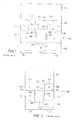
- FIG. 1 depicts a trench MOS-gated device 200 that includes a doped N+ substrate 201 on which is deposited an epitaxial doped upper layer 202.
- Epitaxial layer 202 includes drain region 203, heavily doped P+ body regions 204, and P-well regions 205.
- Abutting body regions 204 in epitaxial layer 203 are heavily doped N+ source regions 206, which are separated from each other by a gate trench 207 that has dielectric sidewalls 208 and floor 209. Contained within trench 207 is a gate material 210, filled to a selected level 211, and an overlying dielectric layer 212. Selected level 211 of gate material 210 is approximately coplanar with the selected depth 216 of N+ source regions 206, thereby providing overlap between source regions 206 and gate material 210. The surface 213 of gate dielectric layer 212 is substantially coplanar with the surface 214 of epitaxial layer 202. Deposited metal layer 215 contacts body regions 204 and source regions 206.
- FIG. 2 depicts an alternative prior art trench MOS-gated device 300 that includes a doped N+ substrate 301, on which is disposed a doped upper layer 302.
- Upper layer 302 includes drain region 303 and P-wells 305.
- Gate trenches 307 each have dielectric sidewalls 308 and a floor 309 and contain conductive gate material 310, filled to a selected level 311, and an overlying dielectric layer 312.
- the surface 313 of gate dielectric layer 312 is substantially coplanar with the surface 314 of upper layer 302.
- Metal layer 315 is deposited on surface 314 to contact body regions 304 and source regions 306.
- the present invention is directed to an MOS power device a substrate that comprises an upper layer having an upper surface and an underlying drain region, a well region of a first conductance type disposed in the upper layer over the drain region, and a plurality of spaced apart buried gates, each of which comprises a trench that extends from the upper surface of the upper layer through the well region into the drain region.
- Each trench comprises an insulating material lining its surface, a conductive material filling its lower portion to a selected level substantially below the upper surface of the upper layer, and an insulating material substantially filling the remainder of the trench.
- a plurality of highly doped source regions of a second conductance type are disposed in the upper layer adjacent the upper portion of each trench, each source region extending from the upper surface to a depth in the upper layer selected to provide overlap between the source regions and the conductive material in the trenches.
- a "V" groove in each of the highly doped source regions extends through the source regions into the well region and terminates in a nadir.
- a highly doped body region of a first conductance type is disposed in the well region adjacent both to the nadir of one or more of the grooves and to adjacent source regions penetrated by the grooves.
- a conductive layer is disposed over the substrate and electrically contacts the body and source regions.
- the present invention is further directed to a process for fabricating an MOS power device that comprises: providing a semiconductor substrate comprising an upper layer that has an upper surface and an underlying drain region, and forming a well region of a first conductance type in the upper layer overlying the drain region.
- a plurality of spaced apart gate trenches, each extending from the upper surface of the upper layer through the well region into the drain region, are formed and lined with an insulating material.
- a lower portion of each said trench is filled with a conductive material to a selected level substantially below the upper surface of the upper layer, and the upper portion of each trench is substantially filled with an insulating material, thereby forming a plurality of trench gates.
- a plurality of highly doped source regions of a second conductance type are formed in the upper layer adjacent the upper portion of each trench, each source region extending from the upper surface to a depth in the upper layer selected to provide overlap between the source regions and the conductive material in the trenches.
- a "U" groove is formed in each of the highly doped source regions, each groove extending through the source region into the well region and terminating in a nadir.
- a highly doped body region of a first conductance type is implanted in the well region adjacent the nadir of one or more of the grooves, and also adjacent source regions penetrated by the grooves.
- a conductive layer is deposited over the substrate for electrically contacting the body and source regions.
- MOS power device of the present invention which is formed by a completely self-aligned process, avoids the loss of channel width and provides reduced channel resistance without sacrificing device ruggedness and dynamic characteristics, as well as SOA.
- FIG. 1 schematically depicts a cross-section of a trench MOS-gated device 200 of the prior art.
- FIG. 2 is a schematic cross-sectional representation of another trench MOS-gated device 300 of the prior art.
- FIG. 3 schematically depict a cross-section of a trench MOS-gated device 600 in accordance with the present invention.
- FIG. 4 is a schematic cross-sectional representation of another trench MOS-gated device 800 of the present invention.
- FIG. 3 is a schematic cross-sectional view of an MOS power device 600 of the present invention.
- Device 600 includes a heavily doped semiconductor substrate 601, which can be monocrystalline silicon, on which is formed a doped upper layer 602 that includes a drain region 603 and well regions 604.
- Upper layer 602 can be epitaxially grown silicon or, for lower voltage devices (ca 12V), a heavily doped portion of substrate 601.
- Well regions 604 are formed in layer 602 by doping into upper layer upper surface 605.
- Gate trenches 607 extend from surface 605 through well regions 604 to drain region 603.
- Trench dielectric sidewalls 608 and floor 609 preferably comprising silicon dioxide, which can be either deposited or grown, are formed in gate trench 607, which is then filled with a conductive gate material 610, which can be, for example, a metal, a silicide, or doped polysilicon, to a selected level 611.
- Filling of trenches 607 is completed by forming an isolation dielectric layer 612, which can be silicon dioxide or BPSG, over conductive gate material 610 in trenches 607 and on surface 605.
- a planarization dielectric etch is performed to re-expose surface 605 without removing dielectric material 612 from trenches 607.
- Surface 613 of dielectric layer 612 in trenches 607 is thereby rendered substantially coplanar with upper surface 605 of layer 602. It may be advantageous, however, to etch surface 613 slightly below surface 605 in order to increase source contact and improve device on-resistance characteristics.
- Source regions 606 are formed by ion implantation and diffusion to a selected depth 614 in well region 604. Because conductive gate material 610 is recessed within gate trench 607 to permit the inclusion of dielectric layer 612 of sufficient thickness to provide gate isolation, diffusions to form source regions 606 must be deep enough to ensure overlap with conductive gate material 610.
- groove 615 extending below depth 614 is etched through each of source regions 606, terminating in a nadir 616 in well region 604.
- groove 615 is V-shaped, comprising two intersecting surfaces 617a and 617b that intersect at an acute angle, preferably about 60 to about 80 degrees. If KOH in propanol-water is used as the etch agent, groove 615 is etched at an angle ⁇ of 54.74 degrees with respect to upper surface 605; in this instance, the angle of intersection of surfaces 617a and 617b is equal to 180 - 2 ⁇ , or about 70.5 degrees.
- a highly doped body region 618 is formed in well region 604 adjacent nadir 618 at also adjacent the source region 606 penetrated by groove 615.
- a high dose about 5x10 15 cm -2 , of boron can be implanted at an angle of 0 degrees, followed by rapid thermal annealing. It should be noted that unlike the discussed prior art, formation of body region 618 in device 600 of the present invention does not require the use of a body mask.
- a metal layer 619 is deposited on substrate 601 to contact body regions 618 and source regions 606.
- Metal (not shown) can be deposited on the reverse side of substrate 601 to provide contact with drain region 603.
- source regions 606 are shown as having N polarity and body regions 618 are depicted as having P polarity in device 600, it is understood that the polarities of these regions can be reversed from those shown in FIG. 3.
- Gate trenches 607 included in a device of the present invention may have an open-cell stripe topology or a closed-cell cellular topology. Furthermore, in the closed- cell cellular topology, the trenches may have a square or, more preferably, a hexagonal configuration.
- device 600 is a power MOSFET, the present invention is applicable to the construction of other MOS-gated devices such as an insulated gate bipolar transistor (IGBT), an MOS-controlled thyristor (MCT), and an accumulation field effect transistor (ACCUFET).
- IGBT insulated gate bipolar transistor
- MCT MOS-controlled thyristor
- ACCUFET accumulation field effect transistor
- FIG. 4 schematically illustrates trench MOS-gated device 800 similar to device 600, except that groove 818, terminating in nadir 816, comprises three intersecting surfaces 817a, 817b, and 817c.
Landscapes
- Thyristors (AREA)
- Electrodes Of Semiconductors (AREA)
Abstract
An MOS power device a substrate comprises an upper layer having an upper surface
and an underlying drain region, a well region of a first conductance type disposed in the
upper layer over the drain region, and a plurality of spaced apart buried gates, each of which
comprises a trench that extends from the upper surface of the upper layer through the well
region into the drain region. Each trench comprises an insulating material lining its surface, a
conductive material filling its lower portion to a selected level substantially below the upper
surface of the upper layer, and an insulating material substantially filling the remainder of the
trench. A plurality of highly doped source regions of a second conductance type are disposed
in the upper layer adjacent the upper portion of each trench, each source region extending
from the upper surface to a depth in the upper layer selected to provide overlap between the
source regions and the conductive material in the trenches. A groove in each of the highly
doped source regions extends through the source regions into the well region and terminates
in a nadir. A highly doped body region of a first conductance type is disposed in the well
region adjacent both to the nadir of one or more of the grooves and to adjacent source
regions penetrated by the grooves. A conductive layer is disposed over the substrate and
electrically contacts the body and source regions. A process for fabricating a device produces
an MOS power device that avoids the loss of channel width and provides reduced channel
resistance without sacrificing device ruggedness and dynamic characteristics.
Description
- The present invention is related to MOS semiconductor devices and, more particularly, to a power MOS semiconductor device with continuous body contact and a wide active channel.
- Co-pending, commonly assigned U.S. Application Serial No. 09/260,411, filed March 1, 1999 by Christopher B. Kocon et al. for MOS-GATED DEVICE HAVING A BURIED GATE AND PROCESS FOR FORMING SAME, the disclosure of which is incorporated herein by reference, describes a device expected to provide high cell packing density through the use of a recessed and buried gate. FIG. 1 (FIG. 2 in Application Serial No. 09/260,411) depicts a trench MOS-
gated device 200 that includes a dopedN+ substrate 201 on which is deposited an epitaxial doped upper layer 202. Epitaxial layer 202 includesdrain region 203, heavily dopedP+ body regions 204, and P-well regions 205.Abutting body regions 204 inepitaxial layer 203 are heavily dopedN+ source regions 206, which are separated from each other by agate trench 207 that hasdielectric sidewalls 208 andfloor 209. Contained withintrench 207 is agate material 210, filled to a selectedlevel 211, and an overlyingdielectric layer 212. Selectedlevel 211 ofgate material 210 is approximately coplanar with the selecteddepth 216 ofN+ source regions 206, thereby providing overlap betweensource regions 206 andgate material 210. Thesurface 213 of gatedielectric layer 212 is substantially coplanar with thesurface 214 of epitaxial layer 202. Depositedmetal layer 215contacts body regions 204 andsource regions 206. - FIG. 2 (FIG. 3B in Application Serial No. 09/260,411) depicts an alternative prior art trench MOS-
gated device 300 that includes a dopedN+ substrate 301, on which is disposed a doped upper layer 302. Upper layer 302 includes drainregion 303 and P-wells 305.N+ source regions 306, formed by ion implantation and diffusion to aselected depth 316 in upper layer 302, are also separated bygate trench 307.Gate trenches 307 each havedielectric sidewalls 308 and afloor 309 and containconductive gate material 310, filled to a selectedlevel 311, and an overlyingdielectric layer 312. Thesurface 313 of gatedielectric layer 312 is substantially coplanar with thesurface 314 of upper layer 302.Metal layer 315 is deposited onsurface 314 to contact body regions 304 andsource regions 306. - Although the just-described prior art structures are expected to provide high cell packing density, the periodic placement of the P+ body regions produces a high series resistance, resulting in degradation of the electro-thermal dynamic characteristics and ruggedness as well as SOA (Safe Operation Area) of the devices. Also, depending on the total area of the P+ body regions, some loss of channel width can result.
- The present invention is directed to an MOS power device a substrate that comprises an upper layer having an upper surface and an underlying drain region, a well region of a first conductance type disposed in the upper layer over the drain region, and a plurality of spaced apart buried gates, each of which comprises a trench that extends from the upper surface of the upper layer through the well region into the drain region. Each trench comprises an insulating material lining its surface, a conductive material filling its lower portion to a selected level substantially below the upper surface of the upper layer, and an insulating material substantially filling the remainder of the trench. A plurality of highly doped source regions of a second conductance type are disposed in the upper layer adjacent the upper portion of each trench, each source region extending from the upper surface to a depth in the upper layer selected to provide overlap between the source regions and the conductive material in the trenches. A "V" groove in each of the highly doped source regions extends through the source regions into the well region and terminates in a nadir. A highly doped body region of a first conductance type is disposed in the well region adjacent both to the nadir of one or more of the grooves and to adjacent source regions penetrated by the grooves. A conductive layer is disposed over the substrate and electrically contacts the body and source regions.
- The present invention is further directed to a process for fabricating an MOS power device that comprises: providing a semiconductor substrate comprising an upper layer that has an upper surface and an underlying drain region, and forming a well region of a first conductance type in the upper layer overlying the drain region. A plurality of spaced apart gate trenches, each extending from the upper surface of the upper layer through the well region into the drain region, are formed and lined with an insulating material. A lower portion of each said trench is filled with a conductive material to a selected level substantially below the upper surface of the upper layer, and the upper portion of each trench is substantially filled with an insulating material, thereby forming a plurality of trench gates.
- A plurality of highly doped source regions of a second conductance type are formed in the upper layer adjacent the upper portion of each trench, each source region extending from the upper surface to a depth in the upper layer selected to provide overlap between the source regions and the conductive material in the trenches. A "U" groove is formed in each of the highly doped source regions, each groove extending through the source region into the well region and terminating in a nadir. A highly doped body region of a first conductance type is implanted in the well region adjacent the nadir of one or more of the grooves, and also adjacent source regions penetrated by the grooves. A conductive layer is deposited over the substrate for electrically contacting the body and source regions.
- The MOS power device of the present invention, which is formed by a completely self-aligned process, avoids the loss of channel width and provides reduced channel resistance without sacrificing device ruggedness and dynamic characteristics, as well as SOA.
- FIG. 1 schematically depicts a cross-section of a trench MOS-
gated device 200 of the prior art. - FIG. 2 is a schematic cross-sectional representation of another trench MOS-
gated device 300 of the prior art. - FIG. 3 schematically depict a cross-section of a trench MOS-
gated device 600 in accordance with the present invention. - FIG. 4 is a schematic cross-sectional representation of another trench MOS-
gated device 800 of the present invention. - FIG. 3 is a schematic cross-sectional view of an
MOS power device 600 of the present invention.Device 600 includes a heavily dopedsemiconductor substrate 601, which can be monocrystalline silicon, on which is formed a dopedupper layer 602 that includes adrain region 603 andwell regions 604.Upper layer 602 can be epitaxially grown silicon or, for lower voltage devices (ca 12V), a heavily doped portion ofsubstrate 601.Well regions 604 are formed inlayer 602 by doping into upper layerupper surface 605. -
Gate trenches 607, formed using a trench mask as known in the art, extend fromsurface 605 throughwell regions 604 to drainregion 603. Trenchdielectric sidewalls 608 andfloor 609, preferably comprising silicon dioxide, which can be either deposited or grown, are formed ingate trench 607, which is then filled with aconductive gate material 610, which can be, for example, a metal, a silicide, or doped polysilicon, to a selected level 611. Filling oftrenches 607 is completed by forming an isolationdielectric layer 612, which can be silicon dioxide or BPSG, overconductive gate material 610 intrenches 607 and onsurface 605. A planarization dielectric etch is performed to re-exposesurface 605 without removingdielectric material 612 fromtrenches 607.Surface 613 ofdielectric layer 612 intrenches 607 is thereby rendered substantially coplanar withupper surface 605 oflayer 602. It may be advantageous, however, to etchsurface 613 slightly belowsurface 605 in order to increase source contact and improve device on-resistance characteristics. -
Source regions 606 are formed by ion implantation and diffusion to a selecteddepth 614 inwell region 604. Becauseconductive gate material 610 is recessed withingate trench 607 to permit the inclusion ofdielectric layer 612 of sufficient thickness to provide gate isolation, diffusions to formsource regions 606 must be deep enough to ensure overlap withconductive gate material 610. - A
groove 615 extending belowdepth 614 is etched through each ofsource regions 606, terminating in a nadir 616 inwell region 604. Preferably,groove 615 is V-shaped, comprising two intersecting surfaces 617a and 617b that intersect at an acute angle, preferably about 60 to about 80 degrees. If KOH in propanol-water is used as the etch agent,groove 615 is etched at an angle of 54.74 degrees with respect toupper surface 605; in this instance, the angle of intersection of surfaces 617a and 617b is equal to 180 - 2, or about 70.5 degrees. - A highly doped
body region 618 is formed inwell region 604adjacent nadir 618 at also adjacent thesource region 606 penetrated bygroove 615. For a P+ body, a high dose, about 5x1015 cm-2, of boron can be implanted at an angle of 0 degrees, followed by rapid thermal annealing. It should be noted that unlike the discussed prior art, formation ofbody region 618 indevice 600 of the present invention does not require the use of a body mask. - A
metal layer 619 is deposited onsubstrate 601 to contactbody regions 618 andsource regions 606. Metal (not shown) can be deposited on the reverse side ofsubstrate 601 to provide contact withdrain region 603. Althoughsource regions 606 are shown as having N polarity andbody regions 618 are depicted as having P polarity indevice 600, it is understood that the polarities of these regions can be reversed from those shown in FIG. 3. -
Gate trenches 607 included in a device of the present invention may have an open-cell stripe topology or a closed-cell cellular topology. Furthermore, in the closed- cell cellular topology, the trenches may have a square or, more preferably, a hexagonal configuration. Althoughdevice 600, as schematically depicted in FIG. 3, is a power MOSFET, the present invention is applicable to the construction of other MOS-gated devices such as an insulated gate bipolar transistor (IGBT), an MOS-controlled thyristor (MCT), and an accumulation field effect transistor (ACCUFET). - Various etch technologies for controlling sidewall angles can be applied to the present invention. FIG. 4 schematically illustrates trench MOS-gated
device 800 similar todevice 600, except that groove 818, terminating innadir 816, comprises three intersectingsurfaces - The invention has been described in detail for the purpose of illustration, but it is understood that such detail is solely for that purpose, and variations can be made therein by those skilled in the art without departing from the spirit and scope of the invention, which is defined by the following claims.
Claims (30)
- An MOS power device comprising:a substrate that comprises an upper layer having an upper surface and an underlying drain region;a well region of a first conductance type disposed in said upper layer overlying said drain region;a plurality of spaced apart buried gates, each said gate comprising a trench extending from said upper surface of said upper layer through said well region into said drain region, each said trench comprising an insulating material lining its surface, a conductive material filling its lower portion to a selected level substantially below the upper surface of the upper layer, and an insulating material substantially filling the remainder of said trench;a plurality of highly doped source regions of a second conductance type disposed in said upper layer adjacent said upper portion of each said trench, each said source region extending from said upper surface to a depth in said upper layer selected to provide overlap between said source regions and said conductive material in said trenches;a groove in each of said highly doped source regions, each said groove extending through said source regions into said well region and terminating in a nadir;a highly doped body region of a first conductance type disposed in said well region adjacent said nadir of one or more of said grooves, said body region also being adjacent source regions penetrated by said grooves; anda conductive layer disposed over said substrate and electrically contacting said body and source regions.
- The MOS power device of claim 1 wherein said grooves are V-shaped, comprising two surfaces that intersect at said nadir, said surfaces being disposed at an acute angle to one another.
- The MOS power device of claim 2 wherein said angle comprises about 60 to about 80 degrees.
- The MOS power device of claim 3 wherein said angle comprises about 54 to about 55 degrees.
- The MOS power device of claim 1 wherein said grooves comprise three or more surfaces.
- The MOS power device of claim 1 wherein said first conductance type is P and said second conductance type is N.
- The MOS power device of claim 1 wherein said first conductance type is N and said second conductance type is P.
- The MOS power device of claim 1 wherein said upper layer comprises an epitaxial layer.
- The MOS power device of claim 1 wherein said upper layer comprises a highly doped portion of said substrate.
- The MOS power device of claim 1 wherein said substrate comprises monocrystalline silicon.
- The MOS power device of claim 1 wherein said insulating material in said trenches comprises silicon dioxide.
- The MOS power device of claim 1 wherein said conductive material in said trenches is selected from the group consisting of a metal, a silicide, and doped polysilicon.
- The MOS power device of claim 1 wherein said device is selected from the group consisting of a power MOSFET, an insulated gate bipolar transistor (IGBT), an MOS-controlled thyristor (MCT), and an accumulation field effect transistor (ACCUFET).
- A process for fabricating an MOS power device comprising:providing a semiconductor substrate comprising an upper layer having an upper surface and an underlying drain region;forming a well region of a first conductance type in said upper layer overlying said drain region;forming a plurality of spaced apart gate trenches, each said trench extending from said upper surface of said upper layer through said well region into said drain region;lining each said trench with an insulating material, filling a lower portion of each said trench with a conductive material to a selected level substantially below the upper surface of the upper layer, and substantially filling the upper portion of each said trench with an insulating material, thereby forming a plurality of trench gates;forming a plurality of highly doped source regions of a second conductance type in said upper layer adjacent said upper portion of each said trench, each said source region extending from said upper surface to a depth in said upper layer selected to provide overlap between said source regions and said conductive material in said trenches;forming a groove in each of said highly doped source regions, each said groove extending through said source regions into said well region and terminating in a nadir;implanting a highly doped body region of a first conductance type in said well region adjacent said nadir of one or more of said grooves, said body region also being adjacent source regions penetrated by said grooves; anddepositing a conductive layer over said substrate for electrically contacting said body and source regions.
- The process of claim 14 wherein said grooves are V-shaped, comprising two surfaces that intersect at said nadir, said surfaces being disposed at an acute angle to one another.
- The process of claim 15 wherein said angle comprises about 60 to about 80 degrees.
- The process of claim 16 wherein said angle comprises about 54 to about 55 degrees.
- The process of claim 14 wherein said grooves comprise three or more surfaces.
- The process of claim 14 wherein said first conductance type is P and said second conductance type is N.
- The process of claim 14 wherein said first conductance type is N and said second conductance type is P.
- The process of claim 14 wherein said upper layer comprises an epitaxial layer.
- The process of claim 14 wherein said upper layer comprises a highly doped portion of said substrate.
- The process of claim 14 wherein said substrate comprises monocrystalline silicon.
- The process of claim 14 wherein said insulating material in said trenches comprises silicon dioxide.
- The process of claim 14 wherein said conductive material in said trenches is selected from the group consisting of a metal, a silicide, and doped polysilicon.
- The process of claim 14 wherein said forming said groove in each of said highly doped source regions comprises etching silicon using KOH in propanol-water.
- The process of claim 14 wherein said implanting a highly doped body region of a first conductance type in said well region comprises implanting a dopant through said groove at an implant angle of 0 degrees.
- The process of claim 27 wherein said implanting said dopant is followed by rapid temperature annealing.
- The process of claim 27 wherein said dopant is boron implanted at a dose of about 5x1015 cm-2.
- The process of claim 14 wherein said device is selected from the group consisting of a power MOSFET, an insulated gate bipolar transistor (IGBT), an MOS-controlled thyristor (MCT), and an accumulation field effect transistor (ACCUFET).
Applications Claiming Priority (2)
| Application Number | Priority Date | Filing Date | Title |
|---|---|---|---|
| US09/624,533 US6445035B1 (en) | 2000-07-24 | 2000-07-24 | Power MOS device with buried gate and groove |
| US624533 | 2000-07-24 |
Publications (1)
| Publication Number | Publication Date |
|---|---|
| EP1176643A2 true EP1176643A2 (en) | 2002-01-30 |
Family
ID=24502357
Family Applications (1)
| Application Number | Title | Priority Date | Filing Date |
|---|---|---|---|
| EP01116709A Withdrawn EP1176643A2 (en) | 2000-07-24 | 2001-07-17 | MOS power semiconductor device having a trench gate and method of making the same |
Country Status (4)
| Country | Link |
|---|---|
| US (2) | US6445035B1 (en) |
| EP (1) | EP1176643A2 (en) |
| JP (1) | JP5065557B2 (en) |
| TW (1) | TW522569B (en) |
Cited By (3)
| Publication number | Priority date | Publication date | Assignee | Title |
|---|---|---|---|---|
| WO2002069394A1 (en) * | 2001-02-27 | 2002-09-06 | Fairchild Semiconductor Corporation | Process for depositing and planarizing bpsg for dense trench mosfet application |
| CN102412266A (en) * | 2011-10-13 | 2012-04-11 | 上海华虹Nec电子有限公司 | Power device structure for improving SOA (service-oriented architecture) capability and manufacturing method thereof |
| CN102945804A (en) * | 2012-12-07 | 2013-02-27 | 株洲南车时代电气股份有限公司 | Method for manufacturing trench gate type IGBT (insulated gate bipolar transistor) chip |
Families Citing this family (38)
| Publication number | Priority date | Publication date | Assignee | Title |
|---|---|---|---|---|
| US6916745B2 (en) * | 2003-05-20 | 2005-07-12 | Fairchild Semiconductor Corporation | Structure and method for forming a trench MOSFET having self-aligned features |
| US6709930B2 (en) * | 2002-06-21 | 2004-03-23 | Siliconix Incorporated | Thicker oxide formation at the trench bottom by selective oxide deposition |
| WO2003046999A1 (en) * | 2001-11-30 | 2003-06-05 | Shindengen Electric Manufacturing Co., Ltd. | Semiconductor device and manufacturing method thereof |
| US20030151092A1 (en) * | 2002-02-11 | 2003-08-14 | Feng-Tso Chien | Power mosfet device with reduced snap-back and being capable of increasing avalanche-breakdown current endurance, and method of manafacturing the same |
| US7012005B2 (en) * | 2002-06-25 | 2006-03-14 | Siliconix Incorporated | Self-aligned differential oxidation in trenches by ion implantation |
| US6943426B2 (en) * | 2002-08-14 | 2005-09-13 | Advanced Analogic Technologies, Inc. | Complementary analog bipolar transistors with trench-constrained isolation diffusion |
| TWI237348B (en) * | 2004-08-26 | 2005-08-01 | Mosel Vitelic Inc | Method of manufacturing trench metal oxide semiconductor field effect transistor |
| US7667264B2 (en) | 2004-09-27 | 2010-02-23 | Alpha And Omega Semiconductor Limited | Shallow source MOSFET |
| JP2006202931A (en) * | 2005-01-20 | 2006-08-03 | Renesas Technology Corp | Semiconductor device and manufacturing method thereof |
| US8362547B2 (en) | 2005-02-11 | 2013-01-29 | Alpha & Omega Semiconductor Limited | MOS device with Schottky barrier controlling layer |
| US8283723B2 (en) * | 2005-02-11 | 2012-10-09 | Alpha & Omega Semiconductor Limited | MOS device with low injection diode |
| US7285822B2 (en) * | 2005-02-11 | 2007-10-23 | Alpha & Omega Semiconductor, Inc. | Power MOS device |
| US7948029B2 (en) | 2005-02-11 | 2011-05-24 | Alpha And Omega Semiconductor Incorporated | MOS device with varying trench depth |
| US8093651B2 (en) * | 2005-02-11 | 2012-01-10 | Alpha & Omega Semiconductor Limited | MOS device with integrated schottky diode in active region contact trench |
| WO2006108011A2 (en) * | 2005-04-06 | 2006-10-12 | Fairchild Semiconductor Corporation | Trenched-gate field effect transistors and methods of forming the same |
| AT504290A2 (en) | 2005-06-10 | 2008-04-15 | Fairchild Semiconductor | FIELD EFFECT TRANSISTOR WITH LOAD BALANCE |
| US8338887B2 (en) | 2005-07-06 | 2012-12-25 | Infineon Technologies Ag | Buried gate transistor |
| WO2007033216A2 (en) * | 2005-09-12 | 2007-03-22 | Beth Israel Deaconess Medical Center | Methods and compositions for the treatment and diagnosis of diseases characterized by vascular leak, hypotension, or a procoagulant state |
| TW200713579A (en) * | 2005-09-26 | 2007-04-01 | Fwu-Iuan Hshieh | Structure for avalanche improvement of ultra high density trench MOSFET |
| KR100714900B1 (en) * | 2006-06-09 | 2007-05-04 | 삼성전자주식회사 | Semiconductor device having a buried gate electrode and a manufacturing method thereof |
| DE102006049043B4 (en) * | 2006-10-18 | 2011-03-17 | Infineon Technologies Austria Ag | Field effect controllable semiconductor device and method for its manufacture |
| US7732842B2 (en) * | 2006-12-06 | 2010-06-08 | Fairchild Semiconductor Corporation | Structure and method for forming a planar schottky contact |
| EP2109892A4 (en) * | 2007-01-09 | 2011-03-23 | Maxpower Semiconductor Inc | SEMICONDUCTOR DEVICE |
| US8304829B2 (en) | 2008-12-08 | 2012-11-06 | Fairchild Semiconductor Corporation | Trench-based power semiconductor devices with increased breakdown voltage characteristics |
| US8174067B2 (en) | 2008-12-08 | 2012-05-08 | Fairchild Semiconductor Corporation | Trench-based power semiconductor devices with increased breakdown voltage characteristics |
| US8227855B2 (en) | 2009-02-09 | 2012-07-24 | Fairchild Semiconductor Corporation | Semiconductor devices with stable and controlled avalanche characteristics and methods of fabricating the same |
| US8148749B2 (en) | 2009-02-19 | 2012-04-03 | Fairchild Semiconductor Corporation | Trench-shielded semiconductor device |
| US8049276B2 (en) | 2009-06-12 | 2011-11-01 | Fairchild Semiconductor Corporation | Reduced process sensitivity of electrode-semiconductor rectifiers |
| WO2011048800A1 (en) * | 2009-10-23 | 2011-04-28 | パナソニック株式会社 | Semiconductor device and process for production thereof |
| JP2011134985A (en) * | 2009-12-25 | 2011-07-07 | Fuji Electric Co Ltd | Trench gate type semiconductor device, and method of manufacturing the same |
| JP2011204808A (en) * | 2010-03-25 | 2011-10-13 | Panasonic Corp | Semiconductor device and method of manufacturing the same |
| CN102184945A (en) * | 2011-05-03 | 2011-09-14 | 成都芯源系统有限公司 | Groove gate type MOSFET device |
| CN102916049B (en) * | 2012-10-30 | 2015-04-22 | 成都芯源系统有限公司 | Semiconductor device including junction field effect transistor and method of manufacturing the same |
| KR101828495B1 (en) | 2013-03-27 | 2018-02-12 | 삼성전자주식회사 | Semiconductor Devices Having a Planar Source Electrode |
| KR101934893B1 (en) | 2013-03-27 | 2019-01-03 | 삼성전자 주식회사 | Method of Fabricating a Semiconductor Device Having a Grooved Source Contact Region |
| CN108231900A (en) * | 2017-12-28 | 2018-06-29 | 中山汉臣电子科技有限公司 | Power semiconductor device and preparation method thereof |
| CN117673082A (en) * | 2022-08-23 | 2024-03-08 | 艾科微电子(深圳)有限公司 | Semiconductor device and manufacturing method thereof |
| US12610605B2 (en) * | 2022-11-28 | 2026-04-21 | Globalfoundries U.S. Inc. | IC structure with gate electrode fully within V-shaped cavity |
Family Cites Families (9)
| Publication number | Priority date | Publication date | Assignee | Title |
|---|---|---|---|---|
| JPH04215456A (en) * | 1990-12-14 | 1992-08-06 | Nikon Corp | Wafer with scribe line, and manufacture thereof |
| JPH0823093A (en) * | 1994-07-08 | 1996-01-23 | Nissan Motor Co Ltd | Semiconductor device and manufacturing method thereof |
| US6236099B1 (en) * | 1996-04-22 | 2001-05-22 | International Rectifier Corp. | Trench MOS device and process for radhard device |
| WO1998012741A1 (en) * | 1996-09-18 | 1998-03-26 | Advanced Micro Devices, Inc. | Short channel non-self aligned vmos field effect transistor |
| US6110799A (en) * | 1997-06-30 | 2000-08-29 | Intersil Corporation | Trench contact process |
| US5909618A (en) * | 1997-07-08 | 1999-06-01 | Micron Technology, Inc. | Method of making memory cell with vertical transistor and buried word and body lines |
| JP3326366B2 (en) * | 1997-08-08 | 2002-09-24 | 三洋電機株式会社 | Semiconductor device and manufacturing method thereof |
| JP3164030B2 (en) * | 1997-09-19 | 2001-05-08 | 日本電気株式会社 | Manufacturing method of vertical field effect transistor |
| CN1166002C (en) * | 1998-04-23 | 2004-09-08 | 国际整流器有限公司 | P-shape channelled metal-oxide semiconductor FET transistor structure |
-
2000
- 2000-07-24 US US09/624,533 patent/US6445035B1/en not_active Expired - Lifetime
-
2001
- 2001-07-16 TW TW091117818A patent/TW522569B/en not_active IP Right Cessation
- 2001-07-17 EP EP01116709A patent/EP1176643A2/en not_active Withdrawn
- 2001-07-23 JP JP2001221780A patent/JP5065557B2/en not_active Expired - Lifetime
-
2002
- 2002-07-16 US US10/195,984 patent/US6638826B2/en not_active Expired - Lifetime
Cited By (4)
| Publication number | Priority date | Publication date | Assignee | Title |
|---|---|---|---|---|
| WO2002069394A1 (en) * | 2001-02-27 | 2002-09-06 | Fairchild Semiconductor Corporation | Process for depositing and planarizing bpsg for dense trench mosfet application |
| CN102412266A (en) * | 2011-10-13 | 2012-04-11 | 上海华虹Nec电子有限公司 | Power device structure for improving SOA (service-oriented architecture) capability and manufacturing method thereof |
| CN102945804A (en) * | 2012-12-07 | 2013-02-27 | 株洲南车时代电气股份有限公司 | Method for manufacturing trench gate type IGBT (insulated gate bipolar transistor) chip |
| CN102945804B (en) * | 2012-12-07 | 2015-04-15 | 株洲南车时代电气股份有限公司 | Method for manufacturing trench gate type IGBT (insulated gate bipolar transistor) chip |
Also Published As
| Publication number | Publication date |
|---|---|
| US6638826B2 (en) | 2003-10-28 |
| JP2002124674A (en) | 2002-04-26 |
| TW522569B (en) | 2003-03-01 |
| US20030011027A1 (en) | 2003-01-16 |
| JP5065557B2 (en) | 2012-11-07 |
| US6445035B1 (en) | 2002-09-03 |
Similar Documents
| Publication | Publication Date | Title |
|---|---|---|
| US6638826B2 (en) | Power MOS device with buried gate | |
| US6916712B2 (en) | MOS-gated device having a buried gate and process for forming same | |
| US6365942B1 (en) | MOS-gated power device with doped polysilicon body and process for forming same | |
| EP1054451B1 (en) | MOS-gated power device and process for forming the same | |
| KR100912995B1 (en) | Manufacturing method of high voltage electric power MOSF having a voltage holding area including doped columns formed by rapid diffusion | |
| JP4088033B2 (en) | Semiconductor device | |
| US6673681B2 (en) | Process for forming MOS-gated power device having segmented trench and extended doping zone | |
| KR100305978B1 (en) | Field-effect trench transistors with lightly doped epitaxial regions on the surface of transistors | |
| US7736976B2 (en) | Method for fabricating a power semiconductor device having a voltage sustaining layer with a terraced trench facilitating formation of floating islands | |
| US6750104B2 (en) | High voltage power MOSFET having a voltage sustaining region that includes doped columns formed by trench etching using an etchant gas that is also a doping source | |
| KR100990294B1 (en) | High voltage power MOSFF containing doped columns | |
| US20060170036A1 (en) | Method of fabricating semiconductor device containing dielectrically isolated PN junction for enhanced breakdown characteristics | |
| US20010022379A1 (en) | Power trench transistor device source region formation using silicon spacer | |
| US6373098B1 (en) | Trench-gated device having trench walls formed by selective epitaxial growth and process for forming device |
Legal Events
| Date | Code | Title | Description |
|---|---|---|---|
| PUAI | Public reference made under article 153(3) epc to a published international application that has entered the european phase |
Free format text: ORIGINAL CODE: 0009012 |
|
| AK | Designated contracting states |
Kind code of ref document: A2 Designated state(s): AT BE CH CY DE DK ES FI FR GB GR IE IT LI LU MC NL PT SE TR |
|
| AX | Request for extension of the european patent |
Free format text: AL;LT;LV;MK;RO;SI |
|
| STAA | Information on the status of an ep patent application or granted ep patent |
Free format text: STATUS: THE APPLICATION HAS BEEN WITHDRAWN |
|
| 18W | Application withdrawn |
Effective date: 20031014 |