EP1176455A1 - A travelling wave optical modulator - Google Patents
A travelling wave optical modulator Download PDFInfo
- Publication number
- EP1176455A1 EP1176455A1 EP01306429A EP01306429A EP1176455A1 EP 1176455 A1 EP1176455 A1 EP 1176455A1 EP 01306429 A EP01306429 A EP 01306429A EP 01306429 A EP01306429 A EP 01306429A EP 1176455 A1 EP1176455 A1 EP 1176455A1
- Authority
- EP
- European Patent Office
- Prior art keywords
- single crystalline
- ferroelectric single
- substrate
- travelling wave
- optical modulator
- Prior art date
- Legal status (The legal status is an assumption and is not a legal conclusion. Google has not performed a legal analysis and makes no representation as to the accuracy of the status listed.)
- Granted
Links
- 230000003287 optical effect Effects 0.000 title claims abstract description 150
- 239000000758 substrate Substances 0.000 claims abstract description 107
- 239000010410 layer Substances 0.000 claims abstract description 62
- 239000012790 adhesive layer Substances 0.000 claims abstract description 33
- 239000011521 glass Substances 0.000 claims description 34
- 239000000463 material Substances 0.000 claims description 29
- 238000004519 manufacturing process Methods 0.000 claims description 26
- 229910000679 solder Inorganic materials 0.000 claims description 21
- 239000011347 resin Substances 0.000 claims description 20
- 229920005989 resin Polymers 0.000 claims description 20
- 238000007747 plating Methods 0.000 claims description 11
- 239000000126 substance Substances 0.000 claims description 10
- 229910021417 amorphous silicon Inorganic materials 0.000 claims description 7
- 238000000034 method Methods 0.000 claims description 6
- 238000012545 processing Methods 0.000 claims description 5
- 239000002178 crystalline material Substances 0.000 claims description 4
- 238000003780 insertion Methods 0.000 description 13
- 230000037431 insertion Effects 0.000 description 13
- 239000013078 crystal Substances 0.000 description 12
- 230000003247 decreasing effect Effects 0.000 description 10
- 239000010931 gold Substances 0.000 description 10
- GQYHUHYESMUTHG-UHFFFAOYSA-N lithium niobate Chemical compound [Li+].[O-][Nb](=O)=O GQYHUHYESMUTHG-UHFFFAOYSA-N 0.000 description 9
- 239000013307 optical fiber Substances 0.000 description 7
- RTAQQCXQSZGOHL-UHFFFAOYSA-N Titanium Chemical compound [Ti] RTAQQCXQSZGOHL-UHFFFAOYSA-N 0.000 description 5
- 229910052737 gold Inorganic materials 0.000 description 5
- 238000004544 sputter deposition Methods 0.000 description 5
- 229910052719 titanium Inorganic materials 0.000 description 5
- 239000010936 titanium Substances 0.000 description 5
- VYPSYNLAJGMNEJ-UHFFFAOYSA-N Silicium dioxide Chemical compound O=[Si]=O VYPSYNLAJGMNEJ-UHFFFAOYSA-N 0.000 description 4
- 238000000313 electron-beam-induced deposition Methods 0.000 description 4
- PCHJSUWPFVWCPO-UHFFFAOYSA-N gold Chemical compound [Au] PCHJSUWPFVWCPO-UHFFFAOYSA-N 0.000 description 4
- 238000000206 photolithography Methods 0.000 description 4
- XAGFODPZIPBFFR-UHFFFAOYSA-N aluminium Chemical compound [Al] XAGFODPZIPBFFR-UHFFFAOYSA-N 0.000 description 3
- 229910052782 aluminium Inorganic materials 0.000 description 3
- 238000009792 diffusion process Methods 0.000 description 3
- 239000003960 organic solvent Substances 0.000 description 3
- 229910052814 silicon oxide Inorganic materials 0.000 description 3
- 238000001039 wet etching Methods 0.000 description 3
- 238000009713 electroplating Methods 0.000 description 2
- 238000005498 polishing Methods 0.000 description 2
- WSMQKESQZFQMFW-UHFFFAOYSA-N 5-methyl-pyrazole-3-carboxylic acid Chemical compound CC1=CC(C(O)=O)=NN1 WSMQKESQZFQMFW-UHFFFAOYSA-N 0.000 description 1
- 239000004593 Epoxy Substances 0.000 description 1
- WHXSMMKQMYFTQS-UHFFFAOYSA-N Lithium Chemical compound [Li] WHXSMMKQMYFTQS-UHFFFAOYSA-N 0.000 description 1
- 229910052581 Si3N4 Inorganic materials 0.000 description 1
- PNEYBMLMFCGWSK-UHFFFAOYSA-N aluminium oxide Inorganic materials [O-2].[O-2].[O-2].[Al+3].[Al+3] PNEYBMLMFCGWSK-UHFFFAOYSA-N 0.000 description 1
- 229910052810 boron oxide Inorganic materials 0.000 description 1
- BRPQOXSCLDDYGP-UHFFFAOYSA-N calcium oxide Chemical compound [O-2].[Ca+2] BRPQOXSCLDDYGP-UHFFFAOYSA-N 0.000 description 1
- 239000000292 calcium oxide Substances 0.000 description 1
- ODINCKMPIJJUCX-UHFFFAOYSA-N calcium oxide Inorganic materials [Ca]=O ODINCKMPIJJUCX-UHFFFAOYSA-N 0.000 description 1
- 239000008119 colloidal silica Substances 0.000 description 1
- 230000000052 comparative effect Effects 0.000 description 1
- 238000000151 deposition Methods 0.000 description 1
- 230000008021 deposition Effects 0.000 description 1
- JKWMSGQKBLHBQQ-UHFFFAOYSA-N diboron trioxide Chemical compound O=BOB=O JKWMSGQKBLHBQQ-UHFFFAOYSA-N 0.000 description 1
- 229910000464 lead oxide Inorganic materials 0.000 description 1
- 229910052744 lithium Inorganic materials 0.000 description 1
- OBTSLRFPKIKXSZ-UHFFFAOYSA-N lithium potassium Chemical compound [Li].[K] OBTSLRFPKIKXSZ-UHFFFAOYSA-N 0.000 description 1
- PSVBHJWAIYBPRO-UHFFFAOYSA-N lithium;niobium(5+);oxygen(2-) Chemical compound [Li+].[O-2].[O-2].[O-2].[Nb+5] PSVBHJWAIYBPRO-UHFFFAOYSA-N 0.000 description 1
- ORUIBWPALBXDOA-UHFFFAOYSA-L magnesium fluoride Chemical compound [F-].[F-].[Mg+2] ORUIBWPALBXDOA-UHFFFAOYSA-L 0.000 description 1
- 229910001635 magnesium fluoride Inorganic materials 0.000 description 1
- 239000000395 magnesium oxide Substances 0.000 description 1
- CPLXHLVBOLITMK-UHFFFAOYSA-N magnesium oxide Inorganic materials [Mg]=O CPLXHLVBOLITMK-UHFFFAOYSA-N 0.000 description 1
- AXZKOIWUVFPNLO-UHFFFAOYSA-N magnesium;oxygen(2-) Chemical compound [O-2].[Mg+2] AXZKOIWUVFPNLO-UHFFFAOYSA-N 0.000 description 1
- 238000012986 modification Methods 0.000 description 1
- 230000004048 modification Effects 0.000 description 1
- TWNQGVIAIRXVLR-UHFFFAOYSA-N oxo(oxoalumanyloxy)alumane Chemical compound O=[Al]O[Al]=O TWNQGVIAIRXVLR-UHFFFAOYSA-N 0.000 description 1
- YEXPOXQUZXUXJW-UHFFFAOYSA-N oxolead Chemical compound [Pb]=O YEXPOXQUZXUXJW-UHFFFAOYSA-N 0.000 description 1
- 238000012805 post-processing Methods 0.000 description 1
- 239000000843 powder Substances 0.000 description 1
- HQVNEWCFYHHQES-UHFFFAOYSA-N silicon nitride Chemical compound N12[Si]34N5[Si]62N3[Si]51N64 HQVNEWCFYHHQES-UHFFFAOYSA-N 0.000 description 1
- 229910052709 silver Inorganic materials 0.000 description 1
- 239000006104 solid solution Substances 0.000 description 1
- 238000007669 thermal treatment Methods 0.000 description 1
Images



Classifications
-
- G—PHYSICS
- G02—OPTICS
- G02F—OPTICAL DEVICES OR ARRANGEMENTS FOR THE CONTROL OF LIGHT BY MODIFICATION OF THE OPTICAL PROPERTIES OF THE MEDIA OF THE ELEMENTS INVOLVED THEREIN; NON-LINEAR OPTICS; FREQUENCY-CHANGING OF LIGHT; OPTICAL LOGIC ELEMENTS; OPTICAL ANALOGUE/DIGITAL CONVERTERS
- G02F1/00—Devices or arrangements for the control of the intensity, colour, phase, polarisation or direction of light arriving from an independent light source, e.g. switching, gating or modulating; Non-linear optics
- G02F1/01—Devices or arrangements for the control of the intensity, colour, phase, polarisation or direction of light arriving from an independent light source, e.g. switching, gating or modulating; Non-linear optics for the control of the intensity, phase, polarisation or colour
- G02F1/21—Devices or arrangements for the control of the intensity, colour, phase, polarisation or direction of light arriving from an independent light source, e.g. switching, gating or modulating; Non-linear optics for the control of the intensity, phase, polarisation or colour by interference
- G02F1/225—Devices or arrangements for the control of the intensity, colour, phase, polarisation or direction of light arriving from an independent light source, e.g. switching, gating or modulating; Non-linear optics for the control of the intensity, phase, polarisation or colour by interference in an optical waveguide structure
- G02F1/2255—Devices or arrangements for the control of the intensity, colour, phase, polarisation or direction of light arriving from an independent light source, e.g. switching, gating or modulating; Non-linear optics for the control of the intensity, phase, polarisation or colour by interference in an optical waveguide structure controlled by a high-frequency electromagnetic component in an electric waveguide structure
-
- G—PHYSICS
- G02—OPTICS
- G02F—OPTICAL DEVICES OR ARRANGEMENTS FOR THE CONTROL OF LIGHT BY MODIFICATION OF THE OPTICAL PROPERTIES OF THE MEDIA OF THE ELEMENTS INVOLVED THEREIN; NON-LINEAR OPTICS; FREQUENCY-CHANGING OF LIGHT; OPTICAL LOGIC ELEMENTS; OPTICAL ANALOGUE/DIGITAL CONVERTERS
- G02F1/00—Devices or arrangements for the control of the intensity, colour, phase, polarisation or direction of light arriving from an independent light source, e.g. switching, gating or modulating; Non-linear optics
- G02F1/01—Devices or arrangements for the control of the intensity, colour, phase, polarisation or direction of light arriving from an independent light source, e.g. switching, gating or modulating; Non-linear optics for the control of the intensity, phase, polarisation or colour
- G02F1/03—Devices or arrangements for the control of the intensity, colour, phase, polarisation or direction of light arriving from an independent light source, e.g. switching, gating or modulating; Non-linear optics for the control of the intensity, phase, polarisation or colour based on ceramics or electro-optical crystals, e.g. exhibiting Pockels effect or Kerr effect
- G02F1/035—Devices or arrangements for the control of the intensity, colour, phase, polarisation or direction of light arriving from an independent light source, e.g. switching, gating or modulating; Non-linear optics for the control of the intensity, phase, polarisation or colour based on ceramics or electro-optical crystals, e.g. exhibiting Pockels effect or Kerr effect in an optical waveguide structure
- G02F1/0356—Devices or arrangements for the control of the intensity, colour, phase, polarisation or direction of light arriving from an independent light source, e.g. switching, gating or modulating; Non-linear optics for the control of the intensity, phase, polarisation or colour based on ceramics or electro-optical crystals, e.g. exhibiting Pockels effect or Kerr effect in an optical waveguide structure controlled by a high-frequency electromagnetic wave component in an electric waveguide structure
Definitions
- This invention relates to A travelling wave-type optical modulator including;
- the resin material room temperature-cured resin, heat-cured resin or ultraviolet-cured resin are exemplified. And, the resin materials have lower dielectric constants, respectively.
- ferroelectric single crystalline layer 4 is etched by photolithography using a given mask, and thus, a ferroelectric single crystalline layer 16 having its thicker parts 5 and its thinner parts 6.
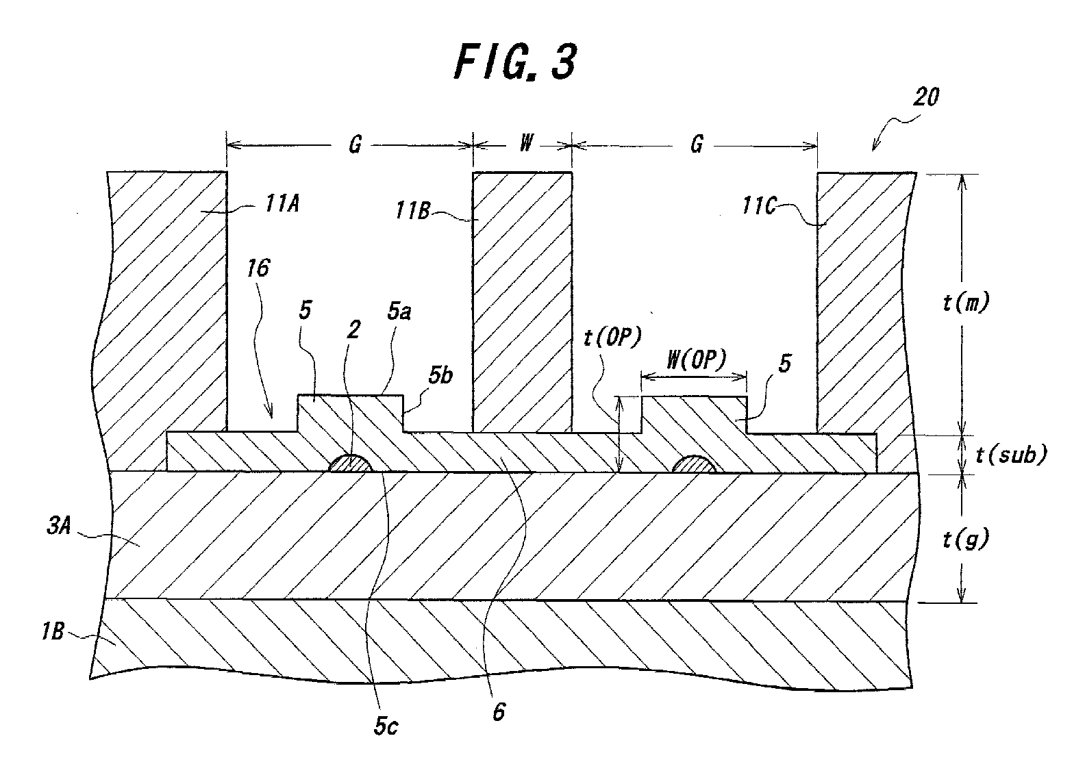
- Numeral references 5a, 5b and 5c denote the top surface, the side surface and the bottom surface of the thicker part 5, respectively.
- the width W of the central electrode 11B was set to 8 ⁇ m, and the width W of the thickness t(OP) of the thicker part 5 was set 6 ⁇ m.
- the electrode gap G was set to 15, 20 and 25 ⁇ m.
- the thickness t(g) of the adhesive layer 3A, the thickness t(sub) of the thinner part 6, the electrode thickness t(m), the microwave refractive index nm, the characteristic impedance Z, the electrode loss ⁇ and the product V ⁇ ⁇ L of operating voltage V ⁇ by electrode length L were investigated. The thus obtained results are listed in Fig. 4.
- optical waveguides 2 are formed on a substrate 1A made of a X-cut ferroelectric single crystal so that the long directions of the optical waveguides 2 are parallel to the Y-direction of the substrate. Therefore, a given TE mode optical wave travels through each optical waveguide in a direction parallel to the Y-direction of the substrate 1A.
- solder glass layer 3 as an adhesive layer is formed on the substrate 1A.
- another supporting substrate 1B is prepared, and a solder glass layer 3 as an adhesive layer is formed on the supporting substrate 1B.
- the solder glass layers 3 are adhered and thermally treated under a given load being applied, to adhere the substrate 1A and the supporting substrate 1B each other, as shown in Fig. 6(b).
- Numeral reference 3A designates an adhesive layer made of the bonded adhesive layers 3.
Landscapes
- Physics & Mathematics (AREA)
- Nonlinear Science (AREA)
- Electromagnetism (AREA)
- General Physics & Mathematics (AREA)
- Optics & Photonics (AREA)
- Chemical & Material Sciences (AREA)
- Engineering & Computer Science (AREA)
- Ceramic Engineering (AREA)
- Crystallography & Structural Chemistry (AREA)
- Optical Modulation, Optical Deflection, Nonlinear Optics, Optical Demodulation, Optical Logic Elements (AREA)
- Optical Integrated Circuits (AREA)
Abstract
Description
- This invention relates to a travelling wave-type optical modulator.
- The inventors disclosed in Japanese Laid-open publication Kokai Hei 10-133159(JPA 10-133159) that if the part under an optical waveguide of a substrate to construct a travelling wave-type optical modulator can be reduced up to e.g. 10 µm or below, the optical modulator can be operated at a frequency of 10 GHz or over without a buffer layer made of silicon oxide or the like. In this case, thicker parts and thinner parts are formed in the substrate, and as a result, the travelling wave-type optical modulator can be operated at a high speed and repressed in DC drift. Moreover, the product (Vπ · L) of operating voltage Vπ by electrode length L in the optical modulator can be favorably decreased.
- Then, the inventors made an attempt to develop the performances of the above optical modulator, and found out the following problem. That is, in the case of connecting the above optical modulator to an external optical fiber, the optical insertion loss was increased. Moreover, it is desired that the product (Vπ·L) is more decreased with keeping the velocity matching for microwave signal and the impedance matching for an external circuit.
- It is an object of the present invention to, in a travelling wave-type optical modulator including such a substrate made of a ferroelectric single crystal as having its thicker parts and thinner parts, decrease the optical insertion loss with keeping the velocity matching for microwave signal and the impedance matching for an external circuit.
- It is another object of the present invention to, in a travelling wave-type optical modulator including such a substrate made of a ferroelectric single crystal as having its thicker parts and thinner parts, to much decrease the product (Vπ · L) of operating voltage Vπ by electrode length L with keeping the velocity matching for microwave signal and the impedance matching for an external circuit.
- This invention relates to A travelling wave-type optical modulator including;
- a supporting substrate,
- a ferroelectric single crystalline layer, on the supporting substrate, having thicker parts and thinner parts within the modulating region of the travelling wave-type optical modulator as viewed in the cross section of the modulating region,
- an optical waveguide formed in the thicker part of the ferroelectric single crystalline layer, and
- electrodes for modulation, each provided on the thinner part of the ferroelectric single crystalline layer in between the adjacent thicker parts.
-
- This invention relates to a method for manufacturing a travelling wave-type optical modulator, including the steps of;
- preparing a substrate made of a ferroelectric single crystalline material,
- forming an optical waveguide in the substrate,
- adhering the substrate to another supporting substrate,
- processing the substrate so as to have thicker parts and thinner parts, as viewed in the cross section of the modulating region, within the modulating region of the travelling wave-type optical modulator and position the optical waveguide in the thicker part, and
- providing electrodes for modulation, each positioned on the thinner part in between the adjacent thicker parts of the ferroelectric single crystalline layer.
-
- According to the above travelling wave-type optical modulator, the optical insertion loss can be decreased with keeping the velocity matching for microwave signal and the impedance matching for an external circuit as described below.
- The optical waveguide can be formed in any area within the thicker part of the ferroelectric single crystalline layer. Preferably, the optical waveguide is formed in an upper area of the thicker part or a lower part thereof adjacent to the supporting substrate. If the waveguide is formed in the lower area, the product (Vπ · L) can be decreased more effectively.
- In a preferred embodiment of the present invention, the supporting substrate includes a base substance made of a hard material and an adhesive layer on the base substance. As the hard material, a ferroelectric single crystal as described below, a glass material and a resin material are exemplified.
The adhesive layer may be made of a glass material having lower dielectric constant and an operation temperature of about 600°C or below. Concretely, solder glass made of plural glass materials such as silicon oxide, lead oxide, aluminum oxide, magnesium oxide, calcium oxide, and boron oxide is exemplified. - As the resin material, room temperature-cured resin, heat-cured resin or ultraviolet-cured resin are exemplified. And, the resin materials have lower dielectric constants, respectively.
- Moreover, this invention relates to a travelling wave-type optical modulator including;
- a supporting substrate,
- ferroelectric single crystalline portions, on the supporting substrate, each separated within the modulating region of the travelling wave-type optical modulator as viewed in the cross section of the modulating region,
- an optical waveguide formed in the ferroelectric single crystalline portion, and
- electrodes for modulation, each provided in between the adjacent ferroelectric single crystalline portions on the supporting substrate.
-
- Furthermore, this invention also relates to a method for manufacturing a travelling wave-type optical modulator, including the steps of;
- preparing a substrate made of a ferroelectric single crystalline material,
- forming an optical waveguide in the substrate,
- adhering the substrate to another supporting substrate,
- processing the substrate to fabricate ferroelectric single crystalline portions, each separated, as viewed in the cross section of the modulating region, within the modulating region of the travelling wave-type optical modulator and so as to position the optical waveguide in the ferroelectric single crystalline portion, and
- providing electrodes for modulation, each positioned in between the adjacent ferroelectric single crystalline portions.
-
- According to the above travelling wave-type optical modulator, the product (Vπ · L) of operating voltage Vπ by electrode length L can be much decreased with keeping the velocity matching for microwave signal and the impedance matching for an external circuit as described below.
- Although the configuration of each ferroelectric single crystalline part is not restricted, it is required that the adjacent ferroelectric single crystalline portions are separated each other, and the electrodes are formed in the spaces in between the adjacent ferroelectric single crystalline portions. Moreover, it is desired that the ferroelectric single crystalline portion is constructed of its bottom surface adjacent to the supporting substrate, its top surface opposite to the supporting substrate and its side surfaces positioned between the bottom surface and the top surface. In this case, each electrode is arranged so as to be contacted with the opposing side surfaces of the adjacent ferroelectric single crystalline parts. Moreover, it is preferable that the top surface is parallel to the bottom surface.
- Particularly, in this case, it is desired that each electrode are contacted with the top surfaces of the adjacent ferroelectric single crystalline portions.
- The optical waveguide may be formed in any area within the ferroelectric single crystalline portion. For example, the optical waveguide may be formed in the upper area or the lower area of the ferroelectric single crystalline portion. If the optical waveguide is formed in the lower area, the product (Vπ · L) of operating voltage Vπ by electrode length L can be much decreased.
- In the above travelling wave-type optical modulator, the supporting substrate preferably includes a base substance made of a hard material and an adhesive layer on the base substance. As the hard material, a ferroelectric single crystal, a glass material and a resin material are exemplified as mentioned above. The adhesive layer may be also made of the above-mentioned solder glass. Moreover, the supporting substrate may be made of a glass material or a resin material entirely.
- The ferroelectric single crystalline portion is made of any material used in the travelling wave-type optical modulator, and concretely, lithium niobate, potassium lithium niobate, lithium tantalate and KTP are exemplified. Preferably, at least one of lithium niobate, lithium tantalate and lithium niobate-lithium tantalate solid solution single crystal is employed.
- For a better understanding of this invention, reference is made to the attached drawings, wherein:
- Figs. 1(a)-(d) are cross sectional views schematically showing the manufacturing steps for a first travelling wave-type optical modulator according to the present invention,
- Figs. 2(a)-(d) are cross sectional views schematically showing the manufacturing steps subsequent to Figs. 1 (a)-(d) for the first travelling wave-type optical modulator,
- Fig. 3 is an enlarged cross sectional view showing a part of the first travelling wave-type optical modulator,
- Fig. 4 is a graph showing the variations in the operating voltage Vπ, the electrode length L, the characteristic impedance Z and the electrode thickness t(m) at speed matching, with several parameters varied, of the first travelling wave-type optical modulator shown in Fig. 3,
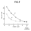
- Fig. 5 is a graph showing the relation between the product (Vπ · L) of operating voltage Vπ by electrode length L and the electrode thickness t(m) in the optical waveguide being formed in the upper area (A) or the lower part (B) of the thicker part of the ferroelectric single crystalline part of the first travelling wave-type optical modulator shown in Fig. 3,
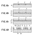
- Figs. 6(a)-(d) are cross sectional views schematically showing the manufacturing steps for a second travelling wave-type optical modulator according to the present invention,
- Figs. 7(a)-(b) are cross sectional views schematically showing the manufacturing steps subsequent to Figs. 6 (a)-(d) for the second travelling wave-type optical modulator,
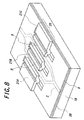
- Fig. 8 is a perspective view showing the second travelling wave-type optical modulator manufactured as shown Figs. 6 and 7,
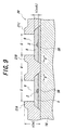
- Fig. 9 is an enlarged cross sectional view showing a part of the second travelling wave-type optical modulator, and
- Fig. 10 is an enlarged cross sectional view showing another second travelling wave-type optical modulator.
-
- This invention is described in detail hereinafter, with reference to the attached drawings.
- Figs. 1(a)-(d) and Fig. 2(a)-(d) are cross sectional views schematically showing the manufacturing steps for a first travelling wave-type optical modulator according to the present invention.
- First of all, as shown in Fig. 1(a),
optical waveguides 2 are formed in asubstrate 1A made of a X-cut ferroelectric single crystal so that the long directions of theoptical waveguides 2 are parallel to the Y-direction of the substrate. Therefore, a given TE mode optical wave travels through each optical waveguide in a direction parallel to the Y-direction of thesubstrate 1A. - Then, an
adhesive layer 3 is formed on thesubstrate 1A. On the other hand, a supportingsubstrate 1B is prepared, and anotheradhesive layer 3 is formed on the supportingsubstrate 1B. Then, as shown in Fig. 1(b), theadhesive layers 3 are contacted each other, and thermally treated under a given load being applied. As a result, thesubstrate 1A and the supportingsubstrate 1B are adhered.Numeral reference 3A designates an adhesive layer made of the bonded adhesive layers 3. Then, thesubstrate 1A is ground and polished to fabricate a thinner ferroelectricsingle crystalline layer 4, as shown in Fig. 1(c). Subsequently, the ferroelectricsingle crystalline layer 4 is etched by photolithography using a given mask, and thus, a ferroelectricsingle crystalline layer 16 having itsthicker parts 5 and itsthinner parts 6.Numeral references thicker part 5, respectively. - Next, after a plating underfilm not shown is formed, a thick resist
layer 7 is formed so as to cover the surface of the ferroelectricsingle crystalline layer 16, as shown in Fig. 2(a). Then,electrodes 11A-11C are formed by plating, as shown in Fig. 2(b). Lastly, the thick resistlayer 7 is removed, and a travelling wave-type optical modulator is fabricated, as shown in Fig. 2(c). Fig. 2(c) shows the cross section of a modulatingregion 20 of the travelling wave-type optical modulator. - The
optical waveguides 2 can be fabricated by a well known method such as a titanium diffusion method, a proton exchange method. Theelectrodes 11A-11C can be made of a material having lower resistance and excellent impedance performance such as Au, Ag, or Cu. Moreover, the electrodes can be made by plating, deposition, sputtering. Moreover, a buffer layer made of silicon oxide, magnesium fluoride, silicon nitride or alumina may be provided. - The
substrate 1A and the supportingsubstrate 1B were made of X-cut lithium niobate single crystal, and a travelling wave-type optical modulator was fabricated as in Figs. 1 and 2. A titanium pattern was formed on asubstrate 1A by photolithography and electron beam deposition, and thermally diffused at 1000-1050°C under moisture-containing oxide atmosphere to form the titanium diffusion typeoptical waveguides 2. - Then, solder glass layers were formed, as
adhesive layers 3, in a thickness of about 5 µm on thesubstrates substrates - Subsequently, the
substrate 1A was ground and polished, and then, CMP-treated by using polishing powders to complete the ferroelectricsingle crystalline layer 4 made of lithium niobate single crystal. Then, an aluminum pattern was aligned and formed immediately on the optical waveguide by photolithograpy and electron beam deposition. Then, the ferroelectricsingle crystalline layer 4 was etched via the aluminum pattern as a mask, to form the ferroelectricsingle crystalline layer 16 having thethicker parts 5 andthinner parts 6. Thereafter, the aluminum pattern was removed. - Then, an underfilm for gold plating, made of a Cr layer as an adhesive layer and a Au layer having a thickness of 5000Å on the Cr layer, was formed by sputtering. Subsequently, a thick resist commercially available was formed, as a guiding layer for gold plating, by photolithography, and then, a gold electrode was formed by electroplating. Thereafter, the resist layer was removed with an organic solvent and the underfilm was removed by wet-etching.
- Then, the thus obtained wafer was cut into chips. The ends of each chip is optically polished to complete a travelling wave-type optical modulator. Thereafter, optical fibers were attached to the traveling wave-type optical modulator with ultraviolet cured resin so that the optical axes of the optical fibers can match the one of the optical waveguide. The transmissive performance (S21) and reflective performance (S11) were measured by a network analyzer, and the microwave reflective index nm, the characteristic impedance Z and the electrode loss α were calculated. Then, the half wavelength voltage Vπ was measured as an electro-optic characteristic. Moreover, the optical insertion loss was measured.
- As shown in Fig. 3, the width W of the
central electrode 11B was set to 8 µm, and the width W of the thickness t(OP) of thethicker part 5 was set 6 µm. Then, the electrode gap G was set to 15, 20 and 25 µm. In this case, the thickness t(g) of theadhesive layer 3A, the thickness t(sub) of thethinner part 6, the electrode thickness t(m), the microwave refractive index nm, the characteristic impedance Z, the electrode loss α and the product Vπ · L of operating voltage Vπ by electrode length L were investigated. The thus obtained results are listed in Fig. 4. - As is apparent from Fig. 4, in the above travelling wave-type optical modulator, the microwave refractive index can be matched to the optical wave refractive index. Particularly, on the condition of the electrode gap G=20 µm, the glass thickness tg=10 µm, the thinner part thickness t(sub)=3 µm, and the electrode thickness t(m)=19 µm, the velocity matching condition was able to be satisfied, and the characteristic impedance Z of 45Ω, the electrode loss α of 0.3dB/cm · (GHz)1/2 were able to be obtained . Moreover, the modulating band of the travelling wave-type optical modulator was 40GHz. The product (Vπ · L) was 8.2 V·cm (the operating voltage Vπ=2.05V, the electrode length L=4 cm). Moreover, the optical insertion loss was 4dB.
- The
substrate 1A and supportingsubstrate 1B were adhered with resin layers, made of epoxy-based resin film (dielectric constant=3.8), formed instead of the solder glass layers. At the time of adhesion, a load of 50 kgf/cm2 was applied, and the resin layers were thermally treated at 170°C. - The thus obtained travelling wave-type optical modulator was evaluated as in Example 1. On the condition of the electrode gap G=20 µm, the resin thickness tg=25 µm, the thinner part thickness t(sub)=3 µm, and the electrode thickness t(m)=19 µm, the velocity matching condition was able to be satisfied, and the characteristic impedance Z of 45Ω, the electrode loss α of 0.3 dB/cm · (GHz)1/2 were able to be obtained. Moreover, the modulating band of the travelling wave-type optical modulator was 40 GHz. The product (Vπ · L) was 8.2 V·cm (the operating voltage Vπ=2.05V, the electrode length L=4cm). Moreover, the optical insertion loss was 4dB.
- Except that the ferroelectric single crystalline layer was formed uniform without the thicker parts and the thinner parts, a travelling wave-type optical modulator was fabricated as in Example 1. The thickness t(sub) of the ferroelectric single crystalline layer was set to 3 µm. As a result, although the modulating band of 40 GHz was attained, the optical insertion loss was increased up to 10 dB.
- On the condition of the width W of the
central electrode 11B = 8 µm, the width W(OP) of thethicker part 5 = 10 µm, the thickness t(OP) of thethicker part 5 = 6 µm, the electrode gap G = 20 µm, the glass thickness t(g)=10 µm and the electrode thickness t(m)=19 µm, a travelling wave-type optical modulator was fabricated. Moreover, the thickness t(sub) of the thinner part was varied as in Fig. 5. In this case, the optical waveguide was formed in an adjacent area to thebottom surface 5c or thetop surface 5a of thethicker part 5. The thus calculated and obtained product (Vπ · L) were shown in Fig. 5 as a graph. - The graph B denotes the product (Vπ · L) in the case of forming the optical waveguide in the area adjacent to the bottom surface 5C, and the graph A denotes the product (Vπ · L) in the case of forming the optical waveguide in the area adjacent to the
top surface 5a. As is apparent from Fig. 5, if the optical waveguide is formed in the are an adjacent to thebottom surface 5c of thethicker part 5, the product (Vπ · L) is more decreased. - Next, the second traveling wave-type optical modulator will be descried with reference to Figs. 6-10.
- First of all, as shown in Fig. 6(a),
optical waveguides 2 are formed on asubstrate 1A made of a X-cut ferroelectric single crystal so that the long directions of theoptical waveguides 2 are parallel to the Y-direction of the substrate. Therefore, a given TE mode optical wave travels through each optical waveguide in a direction parallel to the Y-direction of thesubstrate 1A. - Then, a
solder glass layer 3 as an adhesive layer is formed on thesubstrate 1A. On the other hand, another supportingsubstrate 1B is prepared, and asolder glass layer 3 as an adhesive layer is formed on the supportingsubstrate 1B. Thesolder glass layers 3 are adhered and thermally treated under a given load being applied, to adhere thesubstrate 1A and the supportingsubstrate 1B each other, as shown in Fig. 6(b).Numeral reference 3A designates an adhesive layer made of the bonded adhesive layers 3. - Then, the top surface of the
substrate 1A in which the optical waveguide was formed is ground and polished, thereby to form a thinner ferroelectricsingle crystalline layer 4, as shown in Fig. 6(c). Subsequently, the ferroelectricsingle crystalline layer 4 and thesolder glass layer 3 are partially removed to expose the surface of thesubstrate 1B, thereby to form ferroelectricsingle crystalline portions 8 separately. In this case, a givenspace 9 is formed in between the adjacent ferroelectric single crystalline portions. Then, as shown in Fig. 7(a), an amorphous silicon film is formed so as to cover the surface of each ferroelectricsingle crystalline portion 8 and the exposed surface of thesubstrate 1B. - Then, after a plating underfilm not shown is formed, a thick resist layer is formed, and thereafter,
electrodes 21A-21C are formed by plating. Next, the thick resist layer is removed with an organic solvent, and the plating underfilm is removed by wet-etching to complete a travelling wave-type optical modulator as shown in Fig. 7(b). Fig. 8 is a perspective view schematically showing the travelling wave-type optical modulator. In this embodiment, the travelling wave-type optical modulator constructs a Mach-Zehnder type modulator. Fig. 7(b) corresponds to the cross section of the modulatingregion 20 of the travelling wave-type optical modulator, perpendicular to the long direction of theoptical waveguide 2. - Fig. 9 is an enlarged cross sectional view showing a part of the travelling wave-type optical modulator. As is apparent from Fig. 9, the
electrodes substrate 1B), large effective voltages are applied to theoptical waveguides 2 through the ferroelectricsingle crystalline portions 8. Therefore, the product Vπ · L can be remarkably decreased. - In this example, according to the manufacturing steps shown in Figs. 6 and 7, a travelling wave-type optical modulator having the modulating region as shown in Fig. 9 was be fabricated. Concretely, a titanium pattern was formed on a
substrate 1A made of a X-cut lithium niobate single crystal by photolithography and electron beam deposition, and thermally diffused at 1000-1050°C under a moisture-containing oxide atmosphere, thereby to fabricate a titanium diffusion typeoptical waveguides 2. - Then, an amorphous silicon film was formed in a thickness of 500Å on the
substrate 1A by sputtering, and preferably, asolder glass layer 3 was formed in a thickness of 1000Å successively in the same batch. On the other hand, another supportingsubstrate 1B was prepared, asolder glass 3 was formed in a thickness of 1000Å on the supportingsubstrate 1B by sputtering. Then, thesolder glass layers 3 are contacted and thermally treated at 500°C under a given load being applied to adhere thesubstrates substrate 1B was made of a glass substrate [Bk-7] having an almost the same thermal expansion coefficient as that of the X-cut lithium niobate. As above mentioned, since the supportingsubstrate 1B was adhered to thesubstrate 1B made of the ferroelectric single crystal of lithium niobate, the thus obtained assembly can have a large strength against the post-processing. - Then, the
substrate 1A was ground and polished to form a ferroelectricsingle crystalline layer 4 made of the lithium niobate. Then, the ferroelectricsingle crystalline layer 4 was CMP-treated by polishing powers made of colloidal silica so as to remove the surface damaged layer. Then, the ferroelectricsingle crystalline layer 4 and thesolder glass layer 3A made of the bondedsolder glass layers 3 were partially etched by KrF excimer laser so as to expose the surface of the supportingsubstrate 1B, thereby to fabricate ferroelectricsingle crystalline portions 8. Thereafter, an amorphous silicon film was formed in a thickness of 1500Å so as to cover the ferroelectricsingle crystalline portions 8 and the exposed surface of the supportingsubstrate 1B, and a Cr film as an adhesive layer was formed in a thickness of 500Å successively in the same batch. Then, a Au film as a plating underfilm was formed in a thickness of 300Å on the Cr film. A thick resist layer commercially available was formed as a guiding layer for gold plating, and Au electrodes were fabricated by electro-plating. Thereafter, the thick resist layer was removed by an organic solvent, and the Au layer and Cr layer were removed by wet-etching. - The thus obtained wafer was cut into chips. The ends of each chip is optically polished to complete a travelling wave-type optical modulator. Thereafter, optical fibers were attached to the traveling wave-type optical modulator with ultraviolet cured resin so that the optical axes of the optical fibers can match the one of the optical waveguide. The transmissive performance (S21) and reflective performance (S11) were measured by a network analyzer, and the microwave reflective index nm, the characteristic impedance Z and the electrode loss α were calculated. Then, the half wavelength voltage Vπ was measured as an electro-optic characteristic. Moreover, the optical insertion loss was measured.
- The microwave refractive index can be matched to the optical wave refractive index (nm=no=2.05) at the width W of the
central electrode 21B=30-40 µm, the thickness t(sub) of each ferroelectricsingle crystalline portion 8=6-10 µm, the electrode gap G=30-40 µm, and the thickness t(m) of the electrode= 15-45 µm. - Particularly, on the condition of the width W of the
central electrode 21B=40 µm, the thickness t(sub) of each ferroelectricsingle crystalline portion 8=6 µm, the electrode gap G=30 µm, and the thickness t(m) of the electrode=19 µm, the velocity matching condition can be satisfied, and the characteristic impedance Z of 47Ω, the electrode loss α of 0.18dB/cm · (GHz)1/2 were able to be obtained. Moreover, the modulating band of the travelling wave-type optical modulator was up to 80GHz. The product (Vπ · L) was 9 V·cm (the operating voltage Vπ=2.25V, the electrode length L=4cm). Moreover, the optical insertion loss was 5dB. - In a preferred embodiment of the second travelling wave type optical modulator, the ferroelectric single crystalline portion has a thicker part and a thinner part. An electrode is provided on the thinner part in between the thicker parts of the adjacent ferroelectric single crystalline portions. In this case, the optical insertion loss can be more reduced.
- Fig. 10 is a cross sectional view schematically showing the preferred embodiment of the second travelling wave-type optical modulator. Fundamentally, the travelling wave-type optical modulator has a similar structure to the one as shown in Fig. 9, except that the ferroelectric
single crystalline portion 8A has thethicker part 18 and thethinner part 19. - A travelling wave-type optical modulator as shown in Fig. 10 was fabricated by almost the same manner as in Example 3. The
substrate 1A made of the lithium niobate was ground and polished so as to set the thickness to 10 µm. Then, thesubstrate 1A was partially etched by KrF excimer laser as mentioned above, to fabricate the ferroelectricsingle crystalline portions 8A. The thicker parts and the thinner part were formed by adjusting the laser output and the scanning number. Then, an amorphous silicon layer and Au electrodes were fabricated. - The thus obtained wafer was cut into chips. The ends of each chip is optically polished to complete a travelling wave-type optical modulator. Thereafter, optical fibers were attached to the traveling wave-type optical modulator with ultraviolet cured resin so that the optical axes of the optical fibers can match the one of the optical waveguide. The transmissive performance (S21) and reflective performance (S11) were measured by a network analyzer, and the microwave reflective index nm, the characteristic impedance Z and the electrode loss α were calculated. Then, the half wavelength voltage Vπ was measured as an electro-optic characteristic. Moreover, the optical insertion loss was measured.
- The microwave refractive index was able to be matched to the optical wave refractive index (nm=no=2.15) at the width W of the
central electrode 21B=30-40 µm, the thickness t(sub) of thethinner part 19 of each ferroelectricsingle crystalline portion 8=6-10 µm, the electrode gap G=30-40 µm, and the thickness t(m) of the electrode=15-45 µm. - Particularly, on the condition of the width W of the
central electrode 21B=40 µm, the thickness t(sub) of thethinner part 19 of each ferroelectricsingle crystalline portion 8A=6 µm, the thickness t(OP) of thethicker part 18 of each ferroelectricsingle crystalline portion 8A=10 µm, the electrode gap G=30 µm, and the thickness t(m) of the electrode=19 µm, the velocity matching condition was able to be satisfied, and the characteristic impedance Z of 45Ω, the remarkably reduced electrode loss α of 0.18dB/cm · (GHz)1/2 were able to be obtained. Moreover, the modulating band of the travelling wave-type optical modulator was up to 80GHz. The product (Vπ · L) was 9.5 V · cm. Moreover, the optical insertion loss was 4dB. - Although the present invention was described in detail with reference to the above examples, this invention is not limited to the above disclosure and every kind of variation and modification may be made without departing from the scope of the present invention.
- According to the present invention, in a travelling wave-type optical modulator including such a substrate made of a ferroelectric single crystal as having its thicker parts and thinner parts, the optical insertion loss can be decreased with keeping the velocity matching for microwave signal and the impedance matching for an external circuit. Moreover, the product (Vπ · L) of operating voltage Vπ by electrode length L can be much decreased with keeping the velocity matching for microwave signal and the impedance matching for an external circuit.
Claims (32)
- A travelling wave-type optical modulator comprising;a supporting substrate,a ferroelectric single crystalline layer, on the supporting substrate, having thicker parts and thinner parts within the modulating region of the travelling wave-type optical modulator as viewed in the cross section of the modulating region,an optical waveguide formed in the thicker part of the ferroelectric single crystalline layer, andelectrodes for modulation, each provided on the thinner part of the ferroelectric single crystalline layer in between the adjacent thicker parts.
- A travelling wave-type optical modulator as defined in claim 1, wherein the optical waveguide is formed in the bottom area of the thicker part adjacent to the supporting substrate.
- A travelling wave-type optical modulator as defined in claim 1 or 2, wherein the supporting substrate includes a base substance made of a hard material and an adhesive layer on the base substance to adhere the ferroelectric single crystalline layer.
- A travelling wave-type optical modulator as defined in claim 3, wherein the adhesive layer is made of a glass material or a resin material.
- A travelling wave-type optical modulator as defined in claim 4, wherein the adhesive layer is made of solder glass.
- A method for manufacturing a travelling wave-type optical modulator, comprising the steps of;preparing a substrate made of a ferroelectric single crystalline material,forming an optical waveguide in the substrate,adhering the substrate to another supporting substrate,processing the substrate so as to have thicker parts and thinner parts, as viewed in the cross section of the modulating region, within the modulating region of the travelling wave-type optical modulator and position the optical waveguide in the thicker part, andproviding electrodes for modulation, each positioned on the thinner part in between the adjacent thicker parts of the ferroelectric single crystalline layer.
- A manufacturing method as defined in claim 6, wherein the optical waveguide is positioned in the bottom area of the thicker part adjacent to the supporting substrate.
- A manufacturing method as defined in claim 6 or 7, wherein the substrate is adhered to the supporting substrate by adhering the adhesive layers formed on the substrate and the supporting substrate.
- A manufacturing method as defined in claim 8, wherein each adhesive layer is made of a glass material or a resin material.
- A manufacturing method as defined in claim 9, wherein each adhesive layer is made of solder glass.
- A travelling wave-type optical modulator comprising;a supporting substrate,ferroelectric single crystalline portions, on the supporting substrate, each separated within the modulating region of the travelling wave-type optical modulator as viewed in the cross section of the modulating region,an optical waveguide formed in the ferroelectric single crystalline portion, andelectrodes for modulation, each provided in between the adjacent ferroelectric single crystalline portions on the supporting substrate.
- A travelling wave-type optical modulator as defined in claim 11, wherein the optical waveguide is formed in the bottom area of the ferroelectric single crystalline portion adjacent to the supporting substrate.
- A travelling wave-type optical modulator as defined in claim 11 or 12, wherein each electrode is contacted with at least the side surfaces of the adjacent ferroelectric single crystalline portions.
- A travelling wave-type optical modulator as defined in claim 13, wherein each electrode is contacted with the top surfaces of the adjacent ferroelectric single crystalline portions.
- A travelling wave-type optical modulator as defined in any one of claims 11-14, wherein each ferroelectric single crystalline portion has a thicker part and a thinner part, and each electrode is provided on the thinner parts in between the thicker parts of the adjacent ferroelectric single crystalline portions.
- A travelling wave-type optical modulator as defined in any one of claims 11-15, wherein the supporting substrate includes a base substance made of a hard material and an adhesive layer on the base substance to adhere the ferroelectric single crystalline layer.
- A travelling wave-type optical modulator as defined in claim 16, wherein the adhesive layer is made of a glass material or a resin material.
- A travelling wave-type optical modulator as defined in claim 17, wherein the adhesive layer is made of solder glass.
- A travelling wave-type optical modulator as defined in any one of claims 11-15, wherein the supporting substrate is made of a glass material or a resin material entirely.
- A method for manufacturing a travelling wave-type optical modulator, comprising the steps of;preparing a substrate made of a ferroelectric single crystalline material,forming an optical waveguide in the substrate,adhering the substrate to another supporting substrate,processing the substrate to fabricate ferroelectric single crystalline portions, each separated, as viewed in the cross section of the modulating region, within the modulating region of the travelling wave-type optical modulator and so as to position the optical waveguide in the ferroelectric single crystalline portion, andproviding electrodes for modulation, each positioned in between the adjacent ferroelectric single crystalline portions.
- A manufacturing method as defined in claim 20, wherein the optical waveguide is formed in the bottom area of the ferroelectric single crystalline portion adjacent to the supporting substrate.
- A manufacturing method as defined in claim 20 or 21, wherein each electrode is formed so as to contact with at least the side surfaces of the adjacent ferroelectric single crystalline portions.
- A manufacturing method as defined in claim 22, wherein each electrode is formed so as to be contacted with the top surfaces of the adjacent ferroelectric single crystalline portions.
- A manufacturing method as defined in any one of claims 20-23, wherein a thicker part and a thinner part are formed in each ferroelectric single crystalline portion in processing the substrate, and each electrode is provided on the thinner parts in between the thicker parts of the adjacent ferroelectric single crystalline portions.
- A manufacturing method as defined in any one of claims 20-24, wherein the supporting substrate includes a base substance made of a hard material and an adhesive layer on the base substance to adhere the ferroelectric single crystalline layer.
- A manufacturing method as defined in claim 25, wherein the substrate is adhered to the supporting substrate by adhering the adhesive layers formed on the substrate and the supporting substrate.
- A manufacturing method as defined in claim 26, wherein each adhesive layer is made of a glass material or a resin material.
- A manufacturing method as defined in claim 27, wherein each adhesive layer is made of solder glass.
- A manufacturing method as defined in any one of claims 26-28, wherein after an amorphous silicon film is formed on the substrate, the adhesive layer is formed on the substrate via the amorphous silicon film.
- A manufacturing method as defined in claim 29, wherein the amorphous silicon film and the adhesive layer are formed in the same batch.
- A manufacturing method as defined in any one of claims 20-30, wherein the substrate is processed by excimer laser, thereby to fabricate the ferroelectric single crystalline portions.
- A manufacturing method as defined in claim 31, wherein a Au plating film is formed so as to cover the processed surface of the substrate by the excimer laser, and is processed, thereby to the electrodes.
Priority Applications (1)
| Application Number | Priority Date | Filing Date | Title |
|---|---|---|---|
| EP06016491A EP1722266B1 (en) | 2000-07-27 | 2001-07-26 | A travelling wave-type optical modulator |
Applications Claiming Priority (2)
| Application Number | Priority Date | Filing Date | Title |
|---|---|---|---|
| JP2000226425A JP4443011B2 (en) | 2000-07-27 | 2000-07-27 | Traveling wave type optical modulator |
| JP2000226425 | 2000-07-27 |
Related Child Applications (1)
| Application Number | Title | Priority Date | Filing Date |
|---|---|---|---|
| EP06016491A Division EP1722266B1 (en) | 2000-07-27 | 2001-07-26 | A travelling wave-type optical modulator |
Publications (2)
| Publication Number | Publication Date |
|---|---|
| EP1176455A1 true EP1176455A1 (en) | 2002-01-30 |
| EP1176455B1 EP1176455B1 (en) | 2007-04-18 |
Family
ID=18720045
Family Applications (2)
| Application Number | Title | Priority Date | Filing Date |
|---|---|---|---|
| EP01306429A Expired - Lifetime EP1176455B1 (en) | 2000-07-27 | 2001-07-26 | A travelling wave optical modulator |
| EP06016491A Expired - Lifetime EP1722266B1 (en) | 2000-07-27 | 2001-07-26 | A travelling wave-type optical modulator |
Family Applications After (1)
| Application Number | Title | Priority Date | Filing Date |
|---|---|---|---|
| EP06016491A Expired - Lifetime EP1722266B1 (en) | 2000-07-27 | 2001-07-26 | A travelling wave-type optical modulator |
Country Status (4)
| Country | Link |
|---|---|
| US (1) | US6674565B2 (en) |
| EP (2) | EP1176455B1 (en) |
| JP (1) | JP4443011B2 (en) |
| DE (2) | DE60133498T2 (en) |
Cited By (3)
| Publication number | Priority date | Publication date | Assignee | Title |
|---|---|---|---|---|
| EP1388750A3 (en) * | 2002-08-08 | 2004-09-22 | Ngk Insulators, Ltd. | Optical waveguide devices and travelling wave type optical modulators |
| WO2013186316A1 (en) * | 2012-06-13 | 2013-12-19 | Universite De Nantes | Microwave frequency component controlled by a system of shielded coplanar electrodes, and corresponding manufacturing method |
| CN105974612A (en) * | 2015-03-10 | 2016-09-28 | 国际商业机器公司 | Controlled-capacitance full-depletion interdigitated PIN modulator |
Families Citing this family (43)
| Publication number | Priority date | Publication date | Assignee | Title |
|---|---|---|---|---|
| KR100570586B1 (en) * | 2002-12-17 | 2006-04-13 | (주)아이블포토닉스 | Method for fabricating film structure comprising ferroelectric single crystal layer |
| JP2004219600A (en) * | 2003-01-14 | 2004-08-05 | Ngk Insulators Ltd | Electrode for optical modulation and optical modulator |
| KR100546759B1 (en) * | 2003-08-18 | 2006-01-26 | 한국전자통신연구원 | Distributed Integer Analog Phase Shifter Using Etched Ferroelectric Thin Film and Its Manufacturing Method |
| US7408693B2 (en) * | 2004-07-27 | 2008-08-05 | Jds Uniphase Corporation | Electro-optic device |
| US7444039B2 (en) * | 2005-03-25 | 2008-10-28 | Sumitomo Osaka Cement Co., Ltd. | Optical modulator |
| JP4667932B2 (en) * | 2005-03-31 | 2011-04-13 | 住友大阪セメント株式会社 | Light modulator |
| JP4667933B2 (en) * | 2005-03-31 | 2011-04-13 | 住友大阪セメント株式会社 | Optical element and manufacturing method thereof |
| JP4665134B2 (en) * | 2005-08-08 | 2011-04-06 | 独立行政法人情報通信研究機構 | Fourth harmonic generation system using optical carrier suppressed double sideband modulator |
| JP4759665B2 (en) * | 2005-08-10 | 2011-08-31 | 独立行政法人情報通信研究機構 | Reciprocating frequency modulation system |
| JP4696264B2 (en) * | 2005-08-24 | 2011-06-08 | 独立行政法人情報通信研究機構 | Optical FSK / SSB modulator with intensity balance function |
| JP4631006B2 (en) | 2005-08-24 | 2011-02-16 | 独立行政法人情報通信研究機構 | Automatic adjustment system for FSK modulator |
| JP4547552B2 (en) | 2005-08-31 | 2010-09-22 | 独立行政法人情報通信研究機構 | DSB-SC modulation system capable of erasing carriers and secondary components |
| JP4552032B2 (en) * | 2005-08-31 | 2010-09-29 | 独立行政法人情報通信研究機構 | Optical amplitude modulation system capable of eliminating higher-order components |
| JP4465458B2 (en) | 2005-09-20 | 2010-05-19 | 独立行政法人情報通信研究機構 | Phase control optical FSK modulator |
| JP2007133135A (en) * | 2005-11-10 | 2007-05-31 | Ngk Insulators Ltd | Optical waveguide device |
| JP4771067B2 (en) | 2005-12-01 | 2011-09-14 | 独立行政法人情報通信研究機構 | Optical switch system by optical interference |
| JP4771216B2 (en) | 2006-03-15 | 2011-09-14 | 独立行政法人情報通信研究機構 | Ultra-flat optical frequency comb signal generator |
| JP4183716B2 (en) * | 2006-03-29 | 2008-11-19 | 住友大阪セメント株式会社 | Optical waveguide device |
| US8682177B2 (en) | 2006-06-23 | 2014-03-25 | National Institute Of Information And Communications Technology | Super high speed optical frequency sweeping technology |
| US7844149B2 (en) * | 2007-01-12 | 2010-11-30 | Jds Uniphase Corporation | Humidity tolerant electro-optic device |
| JP5299859B2 (en) | 2008-01-28 | 2013-09-25 | 独立行政法人情報通信研究機構 | Ultra-flat optical frequency comb signal generator |
| JP4909433B2 (en) * | 2010-06-28 | 2012-04-04 | 住友大阪セメント株式会社 | Light modulator |
| JP6033196B2 (en) * | 2013-10-08 | 2016-11-30 | 日本碍子株式会社 | Manufacturing method of optical components |
| KR102311678B1 (en) * | 2014-08-19 | 2021-10-12 | 삼성전자주식회사 | Transmissive optical shutter and method of fabricating the same |
| US10295849B2 (en) | 2016-12-16 | 2019-05-21 | Lumentum Operations Llc | Optical modulator |
| JP7087555B2 (en) * | 2018-03-29 | 2022-06-21 | 住友大阪セメント株式会社 | Optical modulator |
| JP7151593B2 (en) | 2019-03-29 | 2022-10-12 | 住友大阪セメント株式会社 | Optical waveguide element and optical waveguide device |
| US12656637B1 (en) | 2019-11-27 | 2026-06-16 | HyperLight Corporation | Lithium niobate photonic devices having engineered lithium niobate, silicon dioxide, and electrode extension thickness |
| US12282214B2 (en) | 2019-11-27 | 2025-04-22 | HyperLight Corporation | Thin film lithium niobate optical device having an engineered substrate for heterogeneous integration |
| JP7701354B2 (en) | 2019-11-27 | 2025-07-01 | ハイパーライト・コーポレーション | Electro-optical device having improved electrodes |
| US12601938B2 (en) | 2019-11-27 | 2026-04-14 | HyperLight Corporation | Electro-optic devices having closely spaced engineered electrodes |
| JP7428051B2 (en) * | 2020-03-31 | 2024-02-06 | 住友大阪セメント株式会社 | Optical waveguide device and optical modulation device and optical transmitter using the same |
| JP7526583B2 (en) * | 2020-04-21 | 2024-08-01 | 富士通オプティカルコンポーネンツ株式会社 | Optical waveguide device and method for manufacturing optical waveguide device |
| TWI884167B (en) | 2020-05-20 | 2025-05-21 | 日商日本碍子股份有限公司 | Composite substrate for electrooptical element |
| CN115885208A (en) * | 2020-06-02 | 2023-03-31 | 超光公司 | High Performance Optical Modulators and Drivers |
| US11940713B2 (en) * | 2020-11-10 | 2024-03-26 | International Business Machines Corporation | Active electro-optic quantum transducers comprising resonators with switchable nonlinearities |
| JP7729080B2 (en) | 2021-06-11 | 2025-08-26 | 古河ファイテルオプティカルコンポーネンツ株式会社 | Optical devices and optical communication devices |
| JP7658184B2 (en) * | 2021-06-11 | 2025-04-08 | 富士通オプティカルコンポーネンツ株式会社 | Optical devices and optical communication devices |
| CN115524875A (en) * | 2021-06-25 | 2022-12-27 | 苏州极刻光核科技有限公司 | Waveguide line electrode structure and electro-optical modulator |
| JP7677102B2 (en) * | 2021-09-30 | 2025-05-15 | 住友大阪セメント株式会社 | Optical waveguide element, optical modulation device using the same, and optical transmission device |
| US12313920B2 (en) * | 2022-06-14 | 2025-05-27 | HyperLight Corporation | Optical device configured for stress mitigation |
| US12468185B2 (en) * | 2023-05-09 | 2025-11-11 | Nokia Solutions And Networks Oy | Optical waveguide modulator |
| WO2025069334A1 (en) * | 2023-09-28 | 2025-04-03 | 住友大阪セメント株式会社 | Optical waveguide element, optical modulator using same, and optical transmission device |
Citations (3)
| Publication number | Priority date | Publication date | Assignee | Title |
|---|---|---|---|---|
| JPH03229214A (en) * | 1990-02-02 | 1991-10-11 | Nippon Telegr & Teleph Corp <Ntt> | Optical modulation element |
| JPH0651254A (en) * | 1992-08-03 | 1994-02-25 | Nippon Telegr & Teleph Corp <Ntt> | Light control device |
| EP1020754A1 (en) * | 1998-08-10 | 2000-07-19 | Sumitomo Osaka Cement Co., Ltd. | Light modulator of waveguide type |
Family Cites Families (5)
| Publication number | Priority date | Publication date | Assignee | Title |
|---|---|---|---|---|
| KR0134763B1 (en) * | 1992-04-21 | 1998-04-23 | 다니이 아끼오 | Optical waveguide device and manufacturing method |
| US5655041A (en) * | 1995-10-27 | 1997-08-05 | The Trustees Of Princeton University | Method and apparatus for active alignment of semiconductor optical waveguides |
| US5647029A (en) * | 1995-11-27 | 1997-07-08 | Lucent Technologies Inc. | Traveling wave quantum well waveguide modulators using velocity matching for improved frequency performance |
| JP3229214B2 (en) | 1996-08-12 | 2001-11-19 | 三菱重工業株式会社 | Underwater vehicle lifting and lowering operation method and device |
| JP3603977B2 (en) * | 1996-09-06 | 2004-12-22 | 日本碍子株式会社 | Traveling waveform optical modulator and method of manufacturing the same |
-
2000
- 2000-07-27 JP JP2000226425A patent/JP4443011B2/en not_active Expired - Fee Related
-
2001
- 2001-07-24 US US09/911,862 patent/US6674565B2/en not_active Expired - Fee Related
- 2001-07-26 EP EP01306429A patent/EP1176455B1/en not_active Expired - Lifetime
- 2001-07-26 DE DE60133498T patent/DE60133498T2/en not_active Expired - Lifetime
- 2001-07-26 DE DE60127903T patent/DE60127903T2/en not_active Expired - Lifetime
- 2001-07-26 EP EP06016491A patent/EP1722266B1/en not_active Expired - Lifetime
Patent Citations (3)
| Publication number | Priority date | Publication date | Assignee | Title |
|---|---|---|---|---|
| JPH03229214A (en) * | 1990-02-02 | 1991-10-11 | Nippon Telegr & Teleph Corp <Ntt> | Optical modulation element |
| JPH0651254A (en) * | 1992-08-03 | 1994-02-25 | Nippon Telegr & Teleph Corp <Ntt> | Light control device |
| EP1020754A1 (en) * | 1998-08-10 | 2000-07-19 | Sumitomo Osaka Cement Co., Ltd. | Light modulator of waveguide type |
Non-Patent Citations (1)
| Title |
|---|
| ABE N M ET AL: "Analysis of a x-cut Ti:LiNbO/sub 3/ electrooptic modulator with a ridge structure", 1999 SBMO/IEEE MTT-S INTERNATIONAL MICROWAVE AND OPTOELECTRONICS CONFERENCE, 1999 SBMO/IEEE MTT-S INTERNATIONAL MICROWAVE AND OPTOELECTRONICS CONFERENCE, RIO DE JANEIRO, BRAZIL, 9-12 AUG. 1999, 1999, Piscataway, NJ, USA, IEEE, USA, pages 144 - 148 vol. 1, XP002182031, ISBN: 0-7803-5807-4 * |
Cited By (7)
| Publication number | Priority date | Publication date | Assignee | Title |
|---|---|---|---|---|
| EP1388750A3 (en) * | 2002-08-08 | 2004-09-22 | Ngk Insulators, Ltd. | Optical waveguide devices and travelling wave type optical modulators |
| US6950580B2 (en) | 2002-08-08 | 2005-09-27 | Ngk Insulators, Ltd. | Optical waveguide devices and travelling wave type optical modulators |
| WO2013186316A1 (en) * | 2012-06-13 | 2013-12-19 | Universite De Nantes | Microwave frequency component controlled by a system of shielded coplanar electrodes, and corresponding manufacturing method |
| FR2992095A1 (en) * | 2012-06-13 | 2013-12-20 | Univ Nantes | HYPERFREQUENCY COMPONENT CONTROLLED BY A BLOCKED COPLANAR ELECTRODE SYSTEM, AND METHOD OF MANUFACTURING THE SAME |
| US9383595B2 (en) | 2012-06-13 | 2016-07-05 | Universite De Nantes | Microwave frequency component controlled by a system of shielded coplanar electrodes, and corresponding manufacturing method |
| CN105974612A (en) * | 2015-03-10 | 2016-09-28 | 国际商业机器公司 | Controlled-capacitance full-depletion interdigitated PIN modulator |
| CN105974612B (en) * | 2015-03-10 | 2019-05-10 | 国际商业机器公司 | Controlled Capacitance Fully Depleted Interleaved PIN Modulator |
Also Published As
| Publication number | Publication date |
|---|---|
| EP1722266B1 (en) | 2008-04-02 |
| DE60127903D1 (en) | 2007-05-31 |
| DE60133498D1 (en) | 2008-05-15 |
| DE60127903T2 (en) | 2008-01-17 |
| JP4443011B2 (en) | 2010-03-31 |
| EP1722266A2 (en) | 2006-11-15 |
| DE60133498T2 (en) | 2009-05-07 |
| US20020048076A1 (en) | 2002-04-25 |
| US6674565B2 (en) | 2004-01-06 |
| JP2002040381A (en) | 2002-02-06 |
| EP1176455B1 (en) | 2007-04-18 |
| EP1722266A3 (en) | 2006-11-29 |
Similar Documents
| Publication | Publication Date | Title |
|---|---|---|
| US6674565B2 (en) | Travelling wave-type optical modulator | |
| EP1657588B1 (en) | Optical waveguide device and traveling wave type opticalmodulator | |
| EP1291706B1 (en) | An optical waveguide device, an optical modulator, a mounting structure for an optical waveguide device and a supporting member for an optical waveguide substrate | |
| US6556727B2 (en) | Travelling wave-type optical modulator | |
| EP0585565B1 (en) | Optical waveguide device and manufacturing method of the same | |
| US6819851B2 (en) | Optical waveguide device and a travelling-wave optical modulator | |
| US7382942B2 (en) | Optical waveguide devices | |
| EP0813092B1 (en) | Optical waveguide modulator with travelling-wave type electrodes | |
| US7809218B2 (en) | Optical modulators | |
| US6950580B2 (en) | Optical waveguide devices and travelling wave type optical modulators | |
| JP4408558B2 (en) | Traveling waveform optical modulator and method of manufacturing the same | |
| CN100447615C (en) | Optical waveguide device and traveling wave type optical modulator | |
| US7218819B2 (en) | Electrode systems for optical modulation and optical modulators | |
| EP1193536B1 (en) | A travelling wave-type optical modulator | |
| WO2025069334A1 (en) | Optical waveguide element, optical modulator using same, and optical transmission device | |
| JP2004245991A (en) | Optical waveguide device and structure combining the same and optical transmission member | |
| EP1500965A1 (en) | Optical waveguide device with optical modulator and manufacturing method therefor | |
| JPH10239649A (en) | Optical waveguide device | |
| WO2024201876A1 (en) | Optical waveguide element and optical modulation device using same, and optical transmission device | |
| JP2003029223A (en) | Light modulator |
Legal Events
| Date | Code | Title | Description |
|---|---|---|---|
| PUAI | Public reference made under article 153(3) epc to a published international application that has entered the european phase |
Free format text: ORIGINAL CODE: 0009012 |
|
| AK | Designated contracting states |
Kind code of ref document: A1 Designated state(s): DE FR GB IT Kind code of ref document: A1 Designated state(s): AT BE CH CY DE DK ES FI FR GB GR IE IT LI LU MC NL PT SE TR |
|
| AX | Request for extension of the european patent |
Free format text: AL;LT;LV;MK;RO;SI |
|
| 17P | Request for examination filed |
Effective date: 20020718 |
|
| AKX | Designation fees paid |
Free format text: DE FR GB IT |
|
| 17Q | First examination report despatched |
Effective date: 20020930 |
|
| GRAP | Despatch of communication of intention to grant a patent |
Free format text: ORIGINAL CODE: EPIDOSNIGR1 |
|
| GRAS | Grant fee paid |
Free format text: ORIGINAL CODE: EPIDOSNIGR3 |
|
| GRAA | (expected) grant |
Free format text: ORIGINAL CODE: 0009210 |
|
| AK | Designated contracting states |
Kind code of ref document: B1 Designated state(s): DE FR GB IT |
|
| REF | Corresponds to: |
Ref document number: 60127903 Country of ref document: DE Date of ref document: 20070531 Kind code of ref document: P |
|
| ET | Fr: translation filed | ||
| PLBE | No opposition filed within time limit |
Free format text: ORIGINAL CODE: 0009261 |
|
| STAA | Information on the status of an ep patent application or granted ep patent |
Free format text: STATUS: NO OPPOSITION FILED WITHIN TIME LIMIT |
|
| 26N | No opposition filed |
Effective date: 20080121 |
|
| PGFP | Annual fee paid to national office [announced via postgrant information from national office to epo] |
Ref country code: IT Payment date: 20140606 Year of fee payment: 14 |
|
| PGFP | Annual fee paid to national office [announced via postgrant information from national office to epo] |
Ref country code: DE Payment date: 20140724 Year of fee payment: 14 |
|
| PGFP | Annual fee paid to national office [announced via postgrant information from national office to epo] |
Ref country code: FR Payment date: 20140708 Year of fee payment: 14 Ref country code: GB Payment date: 20140723 Year of fee payment: 14 |
|
| REG | Reference to a national code |
Ref country code: DE Ref legal event code: R119 Ref document number: 60127903 Country of ref document: DE |
|
| GBPC | Gb: european patent ceased through non-payment of renewal fee |
Effective date: 20150726 |
|
| PG25 | Lapsed in a contracting state [announced via postgrant information from national office to epo] |
Ref country code: IT Free format text: LAPSE BECAUSE OF NON-PAYMENT OF DUE FEES Effective date: 20150726 Ref country code: DE Free format text: LAPSE BECAUSE OF NON-PAYMENT OF DUE FEES Effective date: 20160202 Ref country code: GB Free format text: LAPSE BECAUSE OF NON-PAYMENT OF DUE FEES Effective date: 20150726 |
|
| REG | Reference to a national code |
Ref country code: FR Ref legal event code: ST Effective date: 20160331 |
|
| PG25 | Lapsed in a contracting state [announced via postgrant information from national office to epo] |
Ref country code: FR Free format text: LAPSE BECAUSE OF NON-PAYMENT OF DUE FEES Effective date: 20150731 |