EP1176128A2 - Composite member comprising bonded different members and method for making the composite member - Google Patents
Composite member comprising bonded different members and method for making the composite member Download PDFInfo
- Publication number
- EP1176128A2 EP1176128A2 EP01306428A EP01306428A EP1176128A2 EP 1176128 A2 EP1176128 A2 EP 1176128A2 EP 01306428 A EP01306428 A EP 01306428A EP 01306428 A EP01306428 A EP 01306428A EP 1176128 A2 EP1176128 A2 EP 1176128A2
- Authority
- EP
- European Patent Office
- Prior art keywords
- solder material
- ceramic base
- composite member
- bonding
- bonding layer
- Prior art date
- Legal status (The legal status is an assumption and is not a legal conclusion. Google has not performed a legal analysis and makes no representation as to the accuracy of the status listed.)
- Granted
Links
- 239000002131 composite material Substances 0.000 title claims abstract description 90
- 238000000034 method Methods 0.000 title claims description 39
- 239000000463 material Substances 0.000 claims abstract description 171
- 229910000679 solder Inorganic materials 0.000 claims abstract description 138
- 239000000919 ceramic Substances 0.000 claims abstract description 85
- 229910052751 metal Inorganic materials 0.000 claims abstract description 71
- 239000002184 metal Substances 0.000 claims abstract description 62
- 239000011888 foil Substances 0.000 claims abstract description 47
- 229910001316 Ag alloy Inorganic materials 0.000 claims abstract description 29
- 239000007790 solid phase Substances 0.000 claims abstract description 21
- 229910052737 gold Inorganic materials 0.000 claims abstract description 8
- PMHQVHHXPFUNSP-UHFFFAOYSA-M copper(1+);methylsulfanylmethane;bromide Chemical compound Br[Cu].CSC PMHQVHHXPFUNSP-UHFFFAOYSA-M 0.000 claims description 51
- 239000004020 conductor Substances 0.000 claims description 40
- 238000010438 heat treatment Methods 0.000 claims description 30
- 229910052759 nickel Inorganic materials 0.000 claims description 21
- 229910045601 alloy Inorganic materials 0.000 claims description 16
- 239000000956 alloy Substances 0.000 claims description 16
- 229910052742 iron Inorganic materials 0.000 claims description 16
- 229910052804 chromium Inorganic materials 0.000 claims description 13
- 238000003825 pressing Methods 0.000 claims description 11
- 229910052721 tungsten Inorganic materials 0.000 claims description 11
- CPLXHLVBOLITMK-UHFFFAOYSA-N Magnesium oxide Chemical compound [Mg]=O CPLXHLVBOLITMK-UHFFFAOYSA-N 0.000 claims description 10
- MCMNRKCIXSYSNV-UHFFFAOYSA-N Zirconium dioxide Chemical compound O=[Zr]=O MCMNRKCIXSYSNV-UHFFFAOYSA-N 0.000 claims description 10
- 229910052750 molybdenum Inorganic materials 0.000 claims description 10
- 239000004065 semiconductor Substances 0.000 claims description 10
- 229910052719 titanium Inorganic materials 0.000 claims description 8
- 229910052581 Si3N4 Inorganic materials 0.000 claims description 5
- PNEYBMLMFCGWSK-UHFFFAOYSA-N aluminium oxide Inorganic materials [O-2].[O-2].[O-2].[Al+3].[Al+3] PNEYBMLMFCGWSK-UHFFFAOYSA-N 0.000 claims description 5
- 229910052735 hafnium Inorganic materials 0.000 claims description 5
- 239000000395 magnesium oxide Substances 0.000 claims description 5
- 229910052758 niobium Inorganic materials 0.000 claims description 5
- HBMJWWWQQXIZIP-UHFFFAOYSA-N silicon carbide Chemical compound [Si+]#[C-] HBMJWWWQQXIZIP-UHFFFAOYSA-N 0.000 claims description 5
- 229910010271 silicon carbide Inorganic materials 0.000 claims description 5
- HQVNEWCFYHHQES-UHFFFAOYSA-N silicon nitride Chemical compound N12[Si]34N5[Si]62N3[Si]51N64 HQVNEWCFYHHQES-UHFFFAOYSA-N 0.000 claims description 5
- 229910052596 spinel Inorganic materials 0.000 claims description 5
- 239000011029 spinel Substances 0.000 claims description 5
- 229910052726 zirconium Inorganic materials 0.000 claims description 5
- 230000035939 shock Effects 0.000 abstract description 12
- 230000035882 stress Effects 0.000 description 30
- 239000006104 solid solution Substances 0.000 description 18
- 238000009792 diffusion process Methods 0.000 description 11
- 230000008646 thermal stress Effects 0.000 description 9
- 230000000694 effects Effects 0.000 description 8
- 230000003647 oxidation Effects 0.000 description 8
- 238000007254 oxidation reaction Methods 0.000 description 8
- 230000000052 comparative effect Effects 0.000 description 7
- 230000005764 inhibitory process Effects 0.000 description 7
- 150000002739 metals Chemical class 0.000 description 7
- 238000005476 soldering Methods 0.000 description 7
- 238000012360 testing method Methods 0.000 description 7
- 235000012431 wafers Nutrition 0.000 description 7
- QVGXLLKOCUKJST-UHFFFAOYSA-N atomic oxygen Chemical compound [O] QVGXLLKOCUKJST-UHFFFAOYSA-N 0.000 description 6
- 239000007795 chemical reaction product Substances 0.000 description 6
- 238000004090 dissolution Methods 0.000 description 6
- 238000009940 knitting Methods 0.000 description 6
- 239000007791 liquid phase Substances 0.000 description 6
- 238000000465 moulding Methods 0.000 description 6
- 229910052760 oxygen Inorganic materials 0.000 description 6
- 239000001301 oxygen Substances 0.000 description 6
- 239000002245 particle Substances 0.000 description 6
- 239000000843 powder Substances 0.000 description 6
- 230000001012 protector Effects 0.000 description 6
- 238000013508 migration Methods 0.000 description 5
- 230000005012 migration Effects 0.000 description 5
- 229910000833 kovar Inorganic materials 0.000 description 4
- 238000004519 manufacturing process Methods 0.000 description 4
- 238000002844 melting Methods 0.000 description 4
- 238000006243 chemical reaction Methods 0.000 description 3
- 238000005336 cracking Methods 0.000 description 3
- 230000007547 defect Effects 0.000 description 3
- 230000006866 deterioration Effects 0.000 description 3
- 230000008018 melting Effects 0.000 description 3
- 239000007769 metal material Substances 0.000 description 3
- 239000000047 product Substances 0.000 description 3
- 230000015572 biosynthetic process Effects 0.000 description 2
- 229910010293 ceramic material Inorganic materials 0.000 description 2
- 238000007796 conventional method Methods 0.000 description 2
- 238000011156 evaluation Methods 0.000 description 2
- 230000000670 limiting effect Effects 0.000 description 2
- 239000000203 mixture Substances 0.000 description 2
- 150000004767 nitrides Chemical class 0.000 description 2
- 230000001590 oxidative effect Effects 0.000 description 2
- 230000036961 partial effect Effects 0.000 description 2
- 230000002040 relaxant effect Effects 0.000 description 2
- 238000000926 separation method Methods 0.000 description 2
- 238000009736 wetting Methods 0.000 description 2
- 229910002701 Ag-Co Inorganic materials 0.000 description 1
- 229910017937 Ag-Ni Inorganic materials 0.000 description 1
- 229910017984 Ag—Ni Inorganic materials 0.000 description 1
- ATJFFYVFTNAWJD-UHFFFAOYSA-N Tin Chemical compound [Sn] ATJFFYVFTNAWJD-UHFFFAOYSA-N 0.000 description 1
- 230000002159 abnormal effect Effects 0.000 description 1
- 238000009825 accumulation Methods 0.000 description 1
- 239000000654 additive Substances 0.000 description 1
- 230000000996 additive effect Effects 0.000 description 1
- 230000002411 adverse Effects 0.000 description 1
- 150000001875 compounds Chemical class 0.000 description 1
- 238000001816 cooling Methods 0.000 description 1
- 230000007797 corrosion Effects 0.000 description 1
- 238000005260 corrosion Methods 0.000 description 1
- 238000005520 cutting process Methods 0.000 description 1
- 230000006378 damage Effects 0.000 description 1
- 230000003292 diminished effect Effects 0.000 description 1
- 230000020169 heat generation Effects 0.000 description 1
- 230000002401 inhibitory effect Effects 0.000 description 1
- 229910000765 intermetallic Inorganic materials 0.000 description 1
- 239000007788 liquid Substances 0.000 description 1
- 230000007774 longterm Effects 0.000 description 1
- 238000002156 mixing Methods 0.000 description 1
- 125000004430 oxygen atom Chemical group O* 0.000 description 1
- 238000006213 oxygenation reaction Methods 0.000 description 1
- 239000012071 phase Substances 0.000 description 1
- 238000010587 phase diagram Methods 0.000 description 1
- 238000007747 plating Methods 0.000 description 1
- 229910052709 silver Inorganic materials 0.000 description 1
- 239000010409 thin film Substances 0.000 description 1
Images




Classifications
-
- C—CHEMISTRY; METALLURGY
- C04—CEMENTS; CONCRETE; ARTIFICIAL STONE; CERAMICS; REFRACTORIES
- C04B—LIME, MAGNESIA; SLAG; CEMENTS; COMPOSITIONS THEREOF, e.g. MORTARS, CONCRETE OR LIKE BUILDING MATERIALS; ARTIFICIAL STONE; CERAMICS; REFRACTORIES; TREATMENT OF NATURAL STONE
- C04B37/00—Joining burned ceramic articles with other burned ceramic articles or other articles by heating
- C04B37/02—Joining burned ceramic articles with other burned ceramic articles or other articles by heating with metallic articles
- C04B37/023—Joining burned ceramic articles with other burned ceramic articles or other articles by heating with metallic articles characterised by the interlayer used
- C04B37/026—Joining burned ceramic articles with other burned ceramic articles or other articles by heating with metallic articles characterised by the interlayer used consisting of metals or metal salts
-
- C—CHEMISTRY; METALLURGY
- C04—CEMENTS; CONCRETE; ARTIFICIAL STONE; CERAMICS; REFRACTORIES
- C04B—LIME, MAGNESIA; SLAG; CEMENTS; COMPOSITIONS THEREOF, e.g. MORTARS, CONCRETE OR LIKE BUILDING MATERIALS; ARTIFICIAL STONE; CERAMICS; REFRACTORIES; TREATMENT OF NATURAL STONE
- C04B2237/00—Aspects relating to ceramic laminates or to joining of ceramic articles with other articles by heating
- C04B2237/02—Aspects relating to interlayers, e.g. used to join ceramic articles with other articles by heating
- C04B2237/12—Metallic interlayers
- C04B2237/122—Metallic interlayers based on refractory metals
-
- C—CHEMISTRY; METALLURGY
- C04—CEMENTS; CONCRETE; ARTIFICIAL STONE; CERAMICS; REFRACTORIES
- C04B—LIME, MAGNESIA; SLAG; CEMENTS; COMPOSITIONS THEREOF, e.g. MORTARS, CONCRETE OR LIKE BUILDING MATERIALS; ARTIFICIAL STONE; CERAMICS; REFRACTORIES; TREATMENT OF NATURAL STONE
- C04B2237/00—Aspects relating to ceramic laminates or to joining of ceramic articles with other articles by heating
- C04B2237/02—Aspects relating to interlayers, e.g. used to join ceramic articles with other articles by heating
- C04B2237/12—Metallic interlayers
- C04B2237/125—Metallic interlayers based on noble metals, e.g. silver
-
- C—CHEMISTRY; METALLURGY
- C04—CEMENTS; CONCRETE; ARTIFICIAL STONE; CERAMICS; REFRACTORIES
- C04B—LIME, MAGNESIA; SLAG; CEMENTS; COMPOSITIONS THEREOF, e.g. MORTARS, CONCRETE OR LIKE BUILDING MATERIALS; ARTIFICIAL STONE; CERAMICS; REFRACTORIES; TREATMENT OF NATURAL STONE
- C04B2237/00—Aspects relating to ceramic laminates or to joining of ceramic articles with other articles by heating
- C04B2237/30—Composition of layers of ceramic laminates or of ceramic or metallic articles to be joined by heating, e.g. Si substrates
- C04B2237/32—Ceramic
- C04B2237/34—Oxidic
-
- C—CHEMISTRY; METALLURGY
- C04—CEMENTS; CONCRETE; ARTIFICIAL STONE; CERAMICS; REFRACTORIES
- C04B—LIME, MAGNESIA; SLAG; CEMENTS; COMPOSITIONS THEREOF, e.g. MORTARS, CONCRETE OR LIKE BUILDING MATERIALS; ARTIFICIAL STONE; CERAMICS; REFRACTORIES; TREATMENT OF NATURAL STONE
- C04B2237/00—Aspects relating to ceramic laminates or to joining of ceramic articles with other articles by heating
- C04B2237/30—Composition of layers of ceramic laminates or of ceramic or metallic articles to be joined by heating, e.g. Si substrates
- C04B2237/32—Ceramic
- C04B2237/34—Oxidic
- C04B2237/343—Alumina or aluminates
-
- C—CHEMISTRY; METALLURGY
- C04—CEMENTS; CONCRETE; ARTIFICIAL STONE; CERAMICS; REFRACTORIES
- C04B—LIME, MAGNESIA; SLAG; CEMENTS; COMPOSITIONS THEREOF, e.g. MORTARS, CONCRETE OR LIKE BUILDING MATERIALS; ARTIFICIAL STONE; CERAMICS; REFRACTORIES; TREATMENT OF NATURAL STONE
- C04B2237/00—Aspects relating to ceramic laminates or to joining of ceramic articles with other articles by heating
- C04B2237/30—Composition of layers of ceramic laminates or of ceramic or metallic articles to be joined by heating, e.g. Si substrates
- C04B2237/32—Ceramic
- C04B2237/34—Oxidic
- C04B2237/345—Refractory metal oxides
- C04B2237/348—Zirconia, hafnia, zirconates or hafnates
-
- C—CHEMISTRY; METALLURGY
- C04—CEMENTS; CONCRETE; ARTIFICIAL STONE; CERAMICS; REFRACTORIES
- C04B—LIME, MAGNESIA; SLAG; CEMENTS; COMPOSITIONS THEREOF, e.g. MORTARS, CONCRETE OR LIKE BUILDING MATERIALS; ARTIFICIAL STONE; CERAMICS; REFRACTORIES; TREATMENT OF NATURAL STONE
- C04B2237/00—Aspects relating to ceramic laminates or to joining of ceramic articles with other articles by heating
- C04B2237/30—Composition of layers of ceramic laminates or of ceramic or metallic articles to be joined by heating, e.g. Si substrates
- C04B2237/32—Ceramic
- C04B2237/36—Non-oxidic
- C04B2237/365—Silicon carbide
-
- C—CHEMISTRY; METALLURGY
- C04—CEMENTS; CONCRETE; ARTIFICIAL STONE; CERAMICS; REFRACTORIES
- C04B—LIME, MAGNESIA; SLAG; CEMENTS; COMPOSITIONS THEREOF, e.g. MORTARS, CONCRETE OR LIKE BUILDING MATERIALS; ARTIFICIAL STONE; CERAMICS; REFRACTORIES; TREATMENT OF NATURAL STONE
- C04B2237/00—Aspects relating to ceramic laminates or to joining of ceramic articles with other articles by heating
- C04B2237/30—Composition of layers of ceramic laminates or of ceramic or metallic articles to be joined by heating, e.g. Si substrates
- C04B2237/32—Ceramic
- C04B2237/36—Non-oxidic
- C04B2237/366—Aluminium nitride
-
- C—CHEMISTRY; METALLURGY
- C04—CEMENTS; CONCRETE; ARTIFICIAL STONE; CERAMICS; REFRACTORIES
- C04B—LIME, MAGNESIA; SLAG; CEMENTS; COMPOSITIONS THEREOF, e.g. MORTARS, CONCRETE OR LIKE BUILDING MATERIALS; ARTIFICIAL STONE; CERAMICS; REFRACTORIES; TREATMENT OF NATURAL STONE
- C04B2237/00—Aspects relating to ceramic laminates or to joining of ceramic articles with other articles by heating
- C04B2237/30—Composition of layers of ceramic laminates or of ceramic or metallic articles to be joined by heating, e.g. Si substrates
- C04B2237/32—Ceramic
- C04B2237/36—Non-oxidic
- C04B2237/368—Silicon nitride
-
- C—CHEMISTRY; METALLURGY
- C04—CEMENTS; CONCRETE; ARTIFICIAL STONE; CERAMICS; REFRACTORIES
- C04B—LIME, MAGNESIA; SLAG; CEMENTS; COMPOSITIONS THEREOF, e.g. MORTARS, CONCRETE OR LIKE BUILDING MATERIALS; ARTIFICIAL STONE; CERAMICS; REFRACTORIES; TREATMENT OF NATURAL STONE
- C04B2237/00—Aspects relating to ceramic laminates or to joining of ceramic articles with other articles by heating
- C04B2237/30—Composition of layers of ceramic laminates or of ceramic or metallic articles to be joined by heating, e.g. Si substrates
- C04B2237/40—Metallic
- C04B2237/403—Refractory metals
-
- C—CHEMISTRY; METALLURGY
- C04—CEMENTS; CONCRETE; ARTIFICIAL STONE; CERAMICS; REFRACTORIES
- C04B—LIME, MAGNESIA; SLAG; CEMENTS; COMPOSITIONS THEREOF, e.g. MORTARS, CONCRETE OR LIKE BUILDING MATERIALS; ARTIFICIAL STONE; CERAMICS; REFRACTORIES; TREATMENT OF NATURAL STONE
- C04B2237/00—Aspects relating to ceramic laminates or to joining of ceramic articles with other articles by heating
- C04B2237/30—Composition of layers of ceramic laminates or of ceramic or metallic articles to be joined by heating, e.g. Si substrates
- C04B2237/40—Metallic
- C04B2237/405—Iron metal group, e.g. Co or Ni
-
- C—CHEMISTRY; METALLURGY
- C04—CEMENTS; CONCRETE; ARTIFICIAL STONE; CERAMICS; REFRACTORIES
- C04B—LIME, MAGNESIA; SLAG; CEMENTS; COMPOSITIONS THEREOF, e.g. MORTARS, CONCRETE OR LIKE BUILDING MATERIALS; ARTIFICIAL STONE; CERAMICS; REFRACTORIES; TREATMENT OF NATURAL STONE
- C04B2237/00—Aspects relating to ceramic laminates or to joining of ceramic articles with other articles by heating
- C04B2237/30—Composition of layers of ceramic laminates or of ceramic or metallic articles to be joined by heating, e.g. Si substrates
- C04B2237/40—Metallic
- C04B2237/405—Iron metal group, e.g. Co or Ni
- C04B2237/406—Iron, e.g. steel
-
- C—CHEMISTRY; METALLURGY
- C04—CEMENTS; CONCRETE; ARTIFICIAL STONE; CERAMICS; REFRACTORIES
- C04B—LIME, MAGNESIA; SLAG; CEMENTS; COMPOSITIONS THEREOF, e.g. MORTARS, CONCRETE OR LIKE BUILDING MATERIALS; ARTIFICIAL STONE; CERAMICS; REFRACTORIES; TREATMENT OF NATURAL STONE
- C04B2237/00—Aspects relating to ceramic laminates or to joining of ceramic articles with other articles by heating
- C04B2237/50—Processing aspects relating to ceramic laminates or to the joining of ceramic articles with other articles by heating
- C04B2237/70—Forming laminates or joined articles comprising layers of a specific, unusual thickness
- C04B2237/708—Forming laminates or joined articles comprising layers of a specific, unusual thickness of one or more of the interlayers
-
- C—CHEMISTRY; METALLURGY
- C04—CEMENTS; CONCRETE; ARTIFICIAL STONE; CERAMICS; REFRACTORIES
- C04B—LIME, MAGNESIA; SLAG; CEMENTS; COMPOSITIONS THEREOF, e.g. MORTARS, CONCRETE OR LIKE BUILDING MATERIALS; ARTIFICIAL STONE; CERAMICS; REFRACTORIES; TREATMENT OF NATURAL STONE
- C04B2237/00—Aspects relating to ceramic laminates or to joining of ceramic articles with other articles by heating
- C04B2237/50—Processing aspects relating to ceramic laminates or to the joining of ceramic articles with other articles by heating
- C04B2237/72—Forming laminates or joined articles comprising at least two interlayers directly next to each other
-
- C—CHEMISTRY; METALLURGY
- C04—CEMENTS; CONCRETE; ARTIFICIAL STONE; CERAMICS; REFRACTORIES
- C04B—LIME, MAGNESIA; SLAG; CEMENTS; COMPOSITIONS THEREOF, e.g. MORTARS, CONCRETE OR LIKE BUILDING MATERIALS; ARTIFICIAL STONE; CERAMICS; REFRACTORIES; TREATMENT OF NATURAL STONE
- C04B2237/00—Aspects relating to ceramic laminates or to joining of ceramic articles with other articles by heating
- C04B2237/50—Processing aspects relating to ceramic laminates or to the joining of ceramic articles with other articles by heating
- C04B2237/80—Joining the largest surface of one substrate with a smaller surface of the other substrate, e.g. butt joining or forming a T-joint
-
- C—CHEMISTRY; METALLURGY
- C04—CEMENTS; CONCRETE; ARTIFICIAL STONE; CERAMICS; REFRACTORIES
- C04B—LIME, MAGNESIA; SLAG; CEMENTS; COMPOSITIONS THEREOF, e.g. MORTARS, CONCRETE OR LIKE BUILDING MATERIALS; ARTIFICIAL STONE; CERAMICS; REFRACTORIES; TREATMENT OF NATURAL STONE
- C04B2237/00—Aspects relating to ceramic laminates or to joining of ceramic articles with other articles by heating
- C04B2237/50—Processing aspects relating to ceramic laminates or to the joining of ceramic articles with other articles by heating
- C04B2237/86—Joining of two substrates at their largest surfaces, one surface being complete joined and covered, the other surface not, e.g. a small plate joined at it's largest surface on top of a larger plate
-
- Y—GENERAL TAGGING OF NEW TECHNOLOGICAL DEVELOPMENTS; GENERAL TAGGING OF CROSS-SECTIONAL TECHNOLOGIES SPANNING OVER SEVERAL SECTIONS OF THE IPC; TECHNICAL SUBJECTS COVERED BY FORMER USPC CROSS-REFERENCE ART COLLECTIONS [XRACs] AND DIGESTS
- Y10—TECHNICAL SUBJECTS COVERED BY FORMER USPC
- Y10T—TECHNICAL SUBJECTS COVERED BY FORMER US CLASSIFICATION
- Y10T428/00—Stock material or miscellaneous articles
- Y10T428/12—All metal or with adjacent metals
- Y10T428/12493—Composite; i.e., plural, adjacent, spatially distinct metal components [e.g., layers, joint, etc.]
- Y10T428/12535—Composite; i.e., plural, adjacent, spatially distinct metal components [e.g., layers, joint, etc.] with additional, spatially distinct nonmetal component
-
- Y—GENERAL TAGGING OF NEW TECHNOLOGICAL DEVELOPMENTS; GENERAL TAGGING OF CROSS-SECTIONAL TECHNOLOGIES SPANNING OVER SEVERAL SECTIONS OF THE IPC; TECHNICAL SUBJECTS COVERED BY FORMER USPC CROSS-REFERENCE ART COLLECTIONS [XRACs] AND DIGESTS
- Y10—TECHNICAL SUBJECTS COVERED BY FORMER USPC
- Y10T—TECHNICAL SUBJECTS COVERED BY FORMER US CLASSIFICATION
- Y10T428/00—Stock material or miscellaneous articles
- Y10T428/12—All metal or with adjacent metals
- Y10T428/12493—Composite; i.e., plural, adjacent, spatially distinct metal components [e.g., layers, joint, etc.]
- Y10T428/12535—Composite; i.e., plural, adjacent, spatially distinct metal components [e.g., layers, joint, etc.] with additional, spatially distinct nonmetal component
- Y10T428/12576—Boride, carbide or nitride component
-
- Y—GENERAL TAGGING OF NEW TECHNOLOGICAL DEVELOPMENTS; GENERAL TAGGING OF CROSS-SECTIONAL TECHNOLOGIES SPANNING OVER SEVERAL SECTIONS OF THE IPC; TECHNICAL SUBJECTS COVERED BY FORMER USPC CROSS-REFERENCE ART COLLECTIONS [XRACs] AND DIGESTS
- Y10—TECHNICAL SUBJECTS COVERED BY FORMER USPC
- Y10T—TECHNICAL SUBJECTS COVERED BY FORMER US CLASSIFICATION
- Y10T428/00—Stock material or miscellaneous articles
- Y10T428/12—All metal or with adjacent metals
- Y10T428/12493—Composite; i.e., plural, adjacent, spatially distinct metal components [e.g., layers, joint, etc.]
- Y10T428/12535—Composite; i.e., plural, adjacent, spatially distinct metal components [e.g., layers, joint, etc.] with additional, spatially distinct nonmetal component
- Y10T428/12611—Oxide-containing component
-
- Y—GENERAL TAGGING OF NEW TECHNOLOGICAL DEVELOPMENTS; GENERAL TAGGING OF CROSS-SECTIONAL TECHNOLOGIES SPANNING OVER SEVERAL SECTIONS OF THE IPC; TECHNICAL SUBJECTS COVERED BY FORMER USPC CROSS-REFERENCE ART COLLECTIONS [XRACs] AND DIGESTS
- Y10—TECHNICAL SUBJECTS COVERED BY FORMER USPC
- Y10T—TECHNICAL SUBJECTS COVERED BY FORMER US CLASSIFICATION
- Y10T428/00—Stock material or miscellaneous articles
- Y10T428/12—All metal or with adjacent metals
- Y10T428/12493—Composite; i.e., plural, adjacent, spatially distinct metal components [e.g., layers, joint, etc.]
- Y10T428/12771—Transition metal-base component
- Y10T428/12806—Refractory [Group IVB, VB, or VIB] metal-base component
- Y10T428/12826—Group VIB metal-base component
- Y10T428/12847—Cr-base component
-
- Y—GENERAL TAGGING OF NEW TECHNOLOGICAL DEVELOPMENTS; GENERAL TAGGING OF CROSS-SECTIONAL TECHNOLOGIES SPANNING OVER SEVERAL SECTIONS OF THE IPC; TECHNICAL SUBJECTS COVERED BY FORMER USPC CROSS-REFERENCE ART COLLECTIONS [XRACs] AND DIGESTS
- Y10—TECHNICAL SUBJECTS COVERED BY FORMER USPC
- Y10T—TECHNICAL SUBJECTS COVERED BY FORMER US CLASSIFICATION
- Y10T428/00—Stock material or miscellaneous articles
- Y10T428/12—All metal or with adjacent metals
- Y10T428/12493—Composite; i.e., plural, adjacent, spatially distinct metal components [e.g., layers, joint, etc.]
- Y10T428/12771—Transition metal-base component
- Y10T428/12861—Group VIII or IB metal-base component
- Y10T428/12889—Au-base component
-
- Y—GENERAL TAGGING OF NEW TECHNOLOGICAL DEVELOPMENTS; GENERAL TAGGING OF CROSS-SECTIONAL TECHNOLOGIES SPANNING OVER SEVERAL SECTIONS OF THE IPC; TECHNICAL SUBJECTS COVERED BY FORMER USPC CROSS-REFERENCE ART COLLECTIONS [XRACs] AND DIGESTS
- Y10—TECHNICAL SUBJECTS COVERED BY FORMER USPC
- Y10T—TECHNICAL SUBJECTS COVERED BY FORMER US CLASSIFICATION
- Y10T428/00—Stock material or miscellaneous articles
- Y10T428/12—All metal or with adjacent metals
- Y10T428/12493—Composite; i.e., plural, adjacent, spatially distinct metal components [e.g., layers, joint, etc.]
- Y10T428/12771—Transition metal-base component
- Y10T428/12861—Group VIII or IB metal-base component
- Y10T428/12931—Co-, Fe-, or Ni-base components, alternative to each other
Definitions
- the present invention relates to a composite member comprising bonded different members, and more particularly to a composite member comprising different members bonded using a specific solder material through solid phase bonding, and a method for making the composite member.
- a method is generally employed according to which the surface of the ceramic base to be bonded is plated with a metal such as Ni to ensure wetting between the ceramic base and the solder material, then these members are disposed opposite to each other with a suitable space, the solder material is poured into the space, and the members are bonded.
- an additive such as Ti which can ensure wetting by forming a reactive layer of a nitride or an oxide on the surface of the ceramic base is added to the solder material, without carrying out the plating with a metal.
- the components constituting the Kovar diffuse into the solder material to form an intermetallic compound layer of low electrical conductivity, which causes deterioration of thermal cycle characteristics and abnormal heat generation at that part.
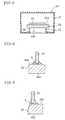
- JP-A-10-209255 discloses a bonding structure of a ceramic base and a connector for power supply which have the structure shown in FIG. 4 as a susceptor for disposing a semiconductor wafer.
- a hole 14 is provided in a ceramic base 1.
- a metallic member 17 such as Mo is exposed which is previously embedded in the ceramic base 1 and has a thermal expansion coefficient approximate to that of the ceramic base 1.
- a cylindrical atmospheric protector 9 is inserted in the hole 14. Inside the atmospheric protector 9, there are inserted a power supplying connector 16 and a low thermal expansion material 15 for stress relaxation.
- the atmospheric protector 9 and the connector 16 are airtightly bonded with a solder material 5, and the low thermal expansion material 15 and the atmospheric protector 9 are airtightly bonded with solder material 5 in respect to the metallic member 17.
- the low thermal expansion material 15 and the metallic member 17 are relaxed in residual stress at bonding and, besides, oxidation of the metallic member 17 such as Mo is inhibited by the atmospheric protector 9, and, hence, even if bonding is performed using a solder material of high proof stress, such as above-mentioned Au-!8Ni solder, cracks are not formed in the ceramic base 1 at bonding and furthermore endurance reliability is high in case the bonded part is exposed to thermal cycle and thermal shock at the time of using high-temperature heater.
- the above bonding structure suffers from the problems that the number of parts increases, and very high production control capacity is required because the metallic member 17 is deteriorated due to oxidation unless the atmospheric protector 9 and the metallic member 17 are completely bonded.
- JP-A-11-278951 discloses a bonded member and a bonding method in which for bonding a corrosion resistant metal ring 23 such as of Kovar to back side 22b of ceramic susceptor 22 in the ceramic base having a structure shown in FIG. 5, these member structures are allowed to have the shapes as shown in FIG. 6 and FIG. 7 for relaxation of the generated thermal stress.
- the solder material changes in properties due to dissolution of the metallic member in the method of bonding the metallic member and the ceramic base by melting the solder material as disclosed in the above patent publication, and the effect to relax the thermal stress is insufficient with giving only such care for the bonding structure as disclosed in the above patent publication, resulting in troubles such as rupture of the ceramic base.
- the present invention has been made in view of the problems in the conventional techniques, and the object is to provide a composite member and a method for making the composite member, according to which a ceramic base having both the thermal cycle characteristics and the thermal shock characteristics and a metallic member are bonded to each other.
- a composite member made by bonding different members namely, a ceramic base and a metallic member, characterized in that an active metal foil is disposed on the surface of the ceramic base and a solder material comprising Au is disposed on the active metal foil, the active metal foil and the solder material are heated to form a bonding layer, the metallic member is disposed on the surface of the bonding layer, and these are pressed and heated to bond the bonding layer and the metallic member through solid phase bonding.
- a composite member made by bonding different members namely, a ceramic base and a metallic member, characterized in that an active metal foil is disposed on the surface of the ceramic base and a solder material comprising an Au-Ag alloy is disposed on the active metal foil, the active metal foil and the solder material are heated to form a bonding layer, the metallic member is disposed on the surface of the bonding layer, and these are pressed and heated to bond the bonding layer and the metallic member through solid phase bonding.
- the proportion of Ag contained in the Au-Ag alloy is 0.5-80 wt%.
- an electrical conductor comprising Mo, W or an alloy of Mo and W is embedded in the ceramic base with a part of the surface of the electrical conductor being exposed to the exterior of the ceramic base, and that the material of the ceramic base is at least one member selected from the group consisting of aluminum nitride, silicon nitride, alumina, zirconia, magnesia, spinel, and silicon carbide.
- the material of the metallic member is at least one metal selected from the group consisting of Ni, Co, Fe and Cr, and it is also preferred that the material of the metallic member is an alloy having as main constituting elements at least one metal selected from the group consisting of Ni, Co, Fe and Cr.
- the material of the active metal foil is at least one metal selected from the group consisting of Ti, Nb, Hf and Zr.
- the composite member made by bonding different members according to the present invention is suitably employed as a susceptor for disposing a semiconductor wafer.
- a method for making a composite member by bonding different members namely, a ceramic base and a metallic member, characterized by including a first step of disposing an active metal foil on the surface of the ceramic base and a solder material comprising Au on the active metal foil and heating them to form a bonding layer comprising the solder material on the surface of the ceramic base, and a second step of disposing the metallic member on the surface of the bonding layer and pressing and heating them to bond the bonding layer and the metallic member through solid phase bonding.
- a method for making a composite member by bonding different members namely, a ceramic base and a metallic member, characterized by including a first step of disposing an active metal foil on the surface of the ceramic base and a solder material comprising an Au-Ag alloy on the active metal foil and heating them to form a bonding layer comprising the solder material on the surface of the ceramic base, and a second step of disposing the metallic member on the surface of the bonding layer and pressing and heating them to bond the bonding layer and the metallic member through solid phase bonding.
- a ceramic base in which an electrical conductor comprising Mo, W or an alloy of Mo and W is embedded in the ceramic base with a part of the surface of the electrical conductor being exposed to the exterior of the ceramic base, and it is preferred to use a ceramic base comprising at least one material selected from the group consisting of aluminum nitride, silicon nitride, alumina, zirconia, magnesia, spinel and silicon carbide.
- a metallic member comprising at least one material selected from the group consisting of Ni, Co, Fe and Cr
- a metallic member comprising an alloy having, as main constituting elements, at least one material selected from the group consisting of Ni, Co, Fe and Cr.
- an active metal foil comprising at least one material selected from the group consisting of Ti, Nb, Hf and Zr.
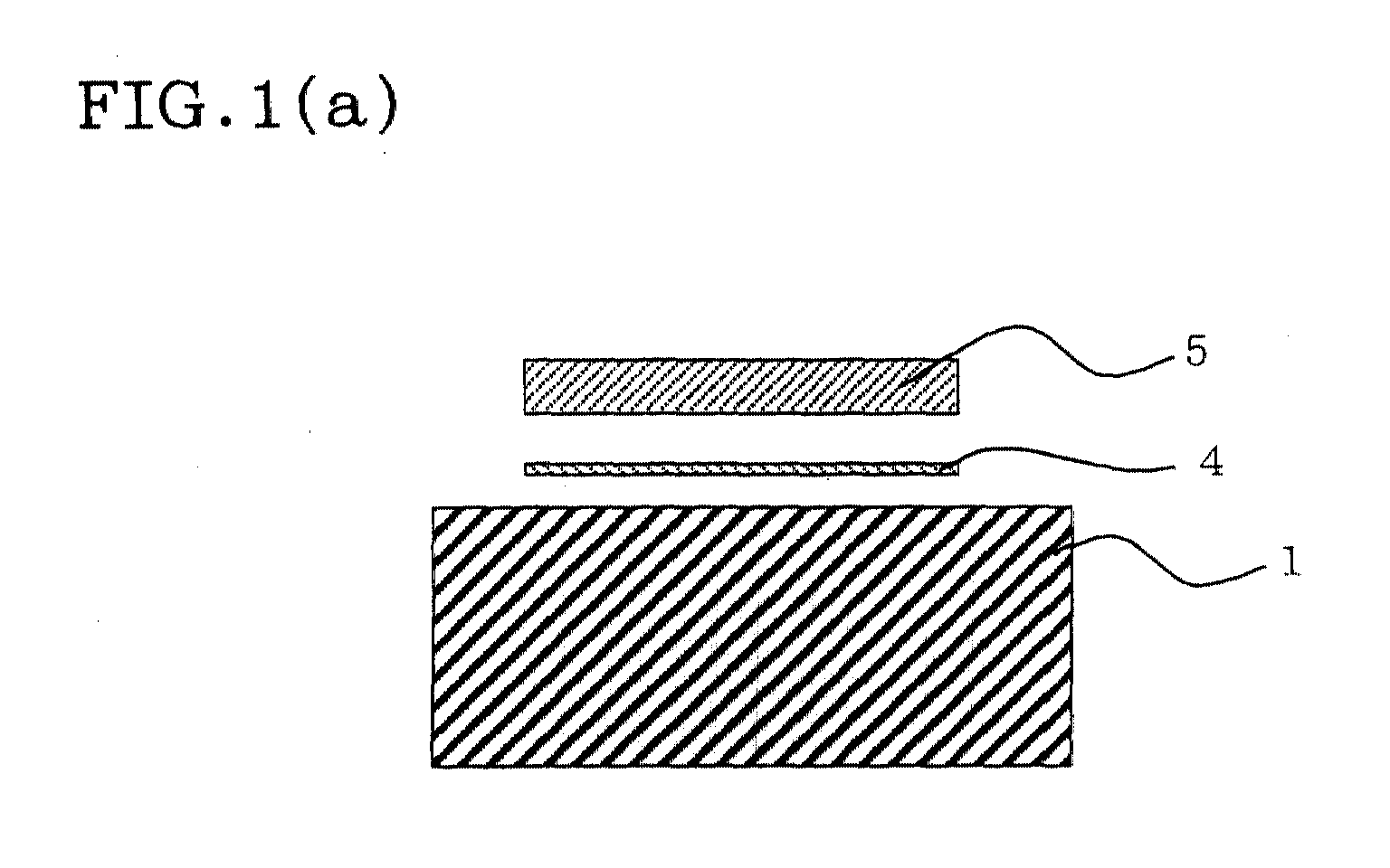
- FIG. 1 (a) and (b) schematically show a first embodiment of the method for making the composite member according to the present invention, and FIG. 1(a) shows the first step and FIG. 1(b) shows the second step.
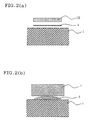
- FIG. 2 (a) and (b) schematically show a second embodiment of the method for making the composite member according to the present invention, and FIG. 2(a) shows the first step and FIG. 2(b) shows the second step.
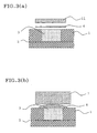
- FIG. 3 (a) and (b) schematically show another embodiment of the method for making the composite member according to the present invention, and FIG. 3(a) shows the first step and FIG. 3(b) shows the second step.
- FIG. 4 is a sectional view which shows one example of bonding structure of a susceptor (conventional one) for disposing a semiconductor wafer.
- FIG. 5 is a sectional view which shows another example of bonding structure of a susceptor (conventional one) for disposing a semiconductor wafer.
- FIG. 6 is a partial sectional view which shows one example of bonding state (conventional) of a ring and a susceptor.
- FIG. 7 is a partial sectional view which shows another example of bonding state (conventional) of a ring and a susceptor.
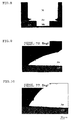
- FIG. 8 is a photograph of metallic texture and ceramic texture which are sectional structures of the composite member made in Example 1.
- FIG. 9 is an enlarged photograph of metallic texture and ceramic texture which are sectional structures around the bonded part of the composite member made in Example 1.
- FIG. 10 is an enlarged photograph of metallic texture and ceramic texture which are sectional structures around the bonded part of the composite member made in Example 1 after subjected to thermal cycle test.
- FIG. 11 is an enlarged photograph of metallic texture and ceramic texture which are sectional structures around the bonded part of the composite member made in Comparative Example 1.
- FIG. 12 is an enlarged photograph of metallic texture and ceramic texture which are sectional structures around the bonded part of the composite member made in Comparative Example 2.
- FIG. 13 is a photograph of metallic texture and ceramic texture which are sectional structures of the composite member made in Example 2.
- FIG. 14 is an enlarged photograph of metallic texture and ceramic texture which are sectional structures around the bonded part of the composite member made in Example 2.
- FIG. 15 is an enlarged photograph of metallic texture and ceramic texture which are sectional structures around the bonded part of the composite member made in Example 2 after subjected to thermal cycle test.
- FIG. 16 is an enlarged photograph of metallic texture and ceramic texture which are sectional structures around the bonded part of the composite member made in Comparative Example 3.
- FIG. 1(a)(b) are schematic views which show the first embodiment of the method for making the composite member by bonding different members of the present invention (hereinafter referred to as "composite member"), and FIG. 1(a) shows the first step and FIG. 1(b) shows the second step.
- an active metal foil 4 and a solder material comprising Au Au solder material 5 are disposed so as to cover a ceramic base 1, followed by heating them to form a bonding layer 6.
- a metallic member 7 is disposed on the surface of the bonding layer 6, and are bonded through solid phase bonding by pressing and heating them, thereby making a composite member.
- the active metal foil 4 used in the first step is active for the ceramic base 1 and forms a reaction product layer at the interface of the ceramic base 1 and the Au solder material 5. Therefore, wettability of the ceramic base 1 with the Au solder material is improved and the bonding layer 6 having satisfactory airtightness is formed. Furthermore, due to the formation of this reaction product layer, the metallic element constituting the active metal foil 4 is almost consumed at the interface and does not remain in the Au solder material 5, and, hence, the phenomenon of increase of proof stress value of the Au solder material 5 does not occur.
- the first embodiment of the present invention is characterized by using the Au solder material.
- Au is a soft metal having low proof stress characteristics and can be a solder material having the feature of relaxing the thermal stress generated by thermal shock through plastic deformation. Accordingly, the composite member of the present invention made using the Au solder material is strong against thermal shock and improved in thermal cycle characteristics.
- FIG. 2(a)(b) are schematic views which show the second embodiment of the method for making the composite member the present invention
- FIG. 2(a) shows the first step
- FIG. 2(b) shows the second step.
- an active metal foil 4 and a solder material comprising an Au-Ag alloy Au-Ag alloy solder material 10
- Au-Ag alloy solder material 10 are disposed so as to cover a ceramic base 1, followed by heating them to form a bonding layer 6.
- a metallic member 7 is disposed on the surface of the bonding layer 6, and are bonded through solid phase bonding by pressing and heating them, thereby making a composite member.
- the active metal foil 4 used in the first step is active for the ceramic base 1 and forms a reaction product layer at the interface of the ceramic base 1 and the Au-Ag alloy solder material 10. Therefore, wettability of the ceramic base 1 with the Au-Ag alloy solder material 10 is improved and the bonding layer 6 having satisfactory airtightness is formed. Furthermore, due to the formation of this reaction product layer, the metallic element constituting the active metal foil 4 is not dissolved in the Au-Ag alloy solder material 10 in the form of solid solution, and the phenomenon of increase of proof stress value of the Au-Ag alloy solder material 10 does not occur.
- the second embodiment of the present invention is characterized by using the Au-Ag alloy solder material comprising Au and Ag which is added to the Au.
- the Au-Ag alloy solder material can be a solder material having the feature of relaxing through plastic deformation the residual stress generated due to the bonding. Accordingly, the composite member of the present invention made using the Au-Ag alloy solder material is strong against thermal shock and good in thermal cycle characteristics.
- the metallic elements constituting the metallic member which have high solid solution formability with Au, but substantially no solid solution formability with Ag, such as Ni, Co, Cr and Fe, are effectively prevented from dissolving in the solder material to form solid solution. Therefore, even when the composite member is used under the temperature conditions of 850-900°C or higher, the metallic element constituting the metallic member does not dissolve in the solder material in the form of solid solution to diffuse therein, namely, the low proof stress value of the bonding layer is not damaged, and thus a composite member having high-temperature endurance can be provided.
- the proportion of Ag contained in Au-Ag alloys used for bonding is preferably 0.5-80 wt%, more preferably 5-40 wt%, and especially preferably 10-30 wt%. This is because if the proportion of Ag is less than 0.5 wt%, the effect to inhibit the dissolution of metallic elements in the form of solid solution cannot be sufficiently exhibited, and if the composite member is used under high temperature conditions, the metallic elements constituting the metallic member dissolves in the solder material to form solid solution. The higher proportion of Ag causes increase of the effect to inhibit dissolution of the metallic elements in the form of solid solution. If the proportion of Ag exceeds 80 wt%, dissolution and diffusion of oxygen atom in the phase of solder material becomes conspicuous, and this is not preferred in case the present bonding method is applied to members which are used in oxidizing atmosphere.
- Amount of the Au solder material or Au-Ag alloy solder material used in the method for making the composite member according to the present invention varies depending on the shape of the bonded part, but may be such that the solder material can cover the disposed active metal foil and can be optionally adjusted within the range where the solder material can be molten by heating. Moreover, in order to reduce residual stress at the time of bonding, it is more preferred that the thickness is not less than 0.3 mm.
- the feature of the metals used as the solder material that the thermal stress is relaxed by plastic deformation is not damaged due to mixing them, and in the case of using Au-Ag alloy solder material, it is never precluded to use them in admixture as far as the effect to inhibit diffusion of the metallic element into the solder material which is imparted by the addition of Ag is not damaged.
- amount of Ti based on the Au solder material or Au-Ag alloy solder material is preferably 0.03-10 wt%, more preferably 0.1-2 wt%. If the amount is less than 0.03 wt%, failure in bonding may occur, and if it is more than 10 wt%, Ti remains in the solder material, resulting in cracking of AlN due to increase in proof stress of the solder material.
- the heating temperature in the second step is preferably a temperature at which solid phase bonding can be performed, namely, a temperature lower than the melting point of the solder material.
- the temperature is preferably 750-1000°C, more preferably 850-950°C.
- the heating temperature is preferably a temperature lower by 50-200°C than the melting point of the solder material, namely, 750-1000°C, though it depends on the amount of Ag.
- the composite member of the present invention is made through bonding steps comprising the first step and the second step, there can be provided a composite member which maintains the low proof stress characteristics of the Au solder material and Au-Ag alloy solder material forming the bonding layer and which is improved in reliability against thermal cycle and thermal shock.
- FIG. 3 schematically shows another embodiment of the method for making the composite member according to the present invention, wherein (a) shows the first step and (b) shows the second step.
- An Mo mesh 2 and an electrical conductor (Mo) 3 disposed so as to be electrically connected to the Mo mesh 2 are embedded in the ceramic base 1.
- an active metal foil 4 and a solder material 11 are disposed so as to cover the surface of the ceramic base 1 and that of the electrical conductor (Mo) 3, followed by heating them to form a bonding layer 6.
- a metallic member 7 is disposed on the surface of the bonding layer 6, followed by performing solid phase bonding by pressing and heating them to make a composite member.
- the active metal foil 4 used in the first step is active for the ceramic base 1 and forms a reaction product layer at the interfaces between the ceramic base 1 and the solder material 11 and between the electrical conductor (Mo) 3 and the solder material 11. Accordingly, wettability of the ceramic base 1 with the solder material 11 is improved and simultaneously airtightness can be secured. As a result, the electrical conductor (Mo) 3 embedded in the ceramic base 1 is not exposed to the air, and, hence, oxidative deterioration of the electrical conductor hardly occurs.
- the "solder material" in FIG. 3(a)(b) may be either Au solder material or Au-Ag solder material.
- material of the ceramic base is preferably at least one selected from the group consisting of aluminum nitride, silicon nitride, alumina, zirconia, magnesia, spinel and silicon carbide.
- the ceramic base may be one which causes occurrence of reaction by heating together with the active metal foil, and the above materials can be used.
- the above materials can constitute the ceramic base each alone or in combination of two or more. Therefore, by optional selection of the ceramic base comprising one of or combination of the above materials, composite members and devices comprising these composite members suitable for the uses such as requiring high heat resistance and high hardness can be provided.
- the material of the metallic member is at least one selected from the group consisting of Ni, Co, Fe and Cr, or an alloy having, as main constituting element, at least one selected from the group consisting of Ni, Co, Fe and Cr.
- These metals or alloys are excellent in oxidation resistance in high temperature areas .
- These metals or components of the alloys do not dissolve in the form of solid solution into the Au solder material or Au-Ag alloy solder material used at the solid phase bonding in the method for making the composite member according to the present invention, and, hence, do not damage the low proof stress characteristics possessed by the solder materials.
- composite members excellent in thermal cycle characteristics and thermal shock characteristics can be provided.
- the alloy having, as main constituting elements, at least one selected from the group consisting of Ni, Co, Fe and Cr means that contents of the metals are such that physical characteristics of the metal of Ni, Co, Fe or Cr are markedly developed and is an alloy having a content of Ni+Co+Fe+Cr of not less than 50 wt%.
- the shape of the metallic member is not limited to one shown in FIG. 1(a)(b), but various shapes such as columnar, square pillar, pyramid, ring and other shapes can be optionally employed.
- these metals or alloys are hardly oxidized in an oxidation resistance test at 800°C in the air, and have an oxidation resistance necessary for the use as metallic terminals for electrical supply of susceptors for disposing semiconductor wafers used in production of semiconductors and, besides, are excellent in electrical conductivity necessary for the use as metallic terminals. Therefore, these metals are preferred from the points that they can constitute the members for high temperature heaters and they are inexpensive and easily available.
- the material of the active metal foil is at least one selected from the group consisting of Ti, Nb, Hf and Zr. Since the active metal foil comprising the above material once dissolves in the solder material to form solid solution and then forms a reaction product such as a nitride with the ceramic base, wettability of the ceramic base with the solder material is improved. Furthermore, by using a suitable amount of the above active metal in the form of a foil, almost all of it is consumed by the reaction at the interface, and substantially no active metal used remains in the solder material.
- proof stress of the solder material can be kept low and thermal stress of the material to be bonded can be diminished by the relaxation effect due to the plastic deformation, and, besides, the trouble that the embedded Mo is exposed to the air can be solved.
- a bonding layer having reliability in airtightness can be formed, and composite members having long-term reliability can be provided.
- the composite member comprising a ceramic base and a metallic member bonded according to the present invention can be suitably employed as a susceptor for disposing a semiconductor wafer in apparatuses for producing semiconductors utilizing its excellent thermal cycle characteristics and thermal shock resistance, more specifically, as a composite member incorporated in devices which exhibit electrostatic chuck function and heater function by metallic electrodes or metallic heaters contained therein.
- an Mo mesh (a wire mesh prepared by knitting Mo wires of 0.12 mm ⁇ in diameter at a density of 50 wires per 1 inch) and an electrical conductor (a molded body obtained by molding Mo powders of 1-100 ⁇ m in particle diameter: 3 mm ⁇ in diameter) which was electrically connected to the Mo mesh, and the portion of the AlN base in which the electrical conductor was embedded was bored, thereby exposing the electrical conductor.
- Example Nos. 4-6 three samples (Sample Nos. 4-6) in total were prepared in the same manner as above, except that the time for bonding the Ni terminal was 10 minutes.
- the composite members of the present invention made by the above method had no cracks in the AlN base as shown in FIG. 9. It is considered that this is because Ni and Ti did not dissolve in the pure Au solder material in the form of solid solution and the low proof stress characteristics of the pure Au solder material was maintained, whereby the stress generated due to the difference in thermal expansion coefficient of the pure Au solder material and the AlN base could be relaxed.
- Sample Nos. 4-6 were subjected to a thermal cycle test of 100 cycles at 700°C, and, thereafter, tensile strength thereof was measured. The results are shown in Table 2. An enlarged photograph of sectional structure of the bonded part after carrying out the thermal cycle test is shown in FIG. 10.
- Sample no. Soldering condition Ni-terminal boding conditions
- Thermal cycle test conditions 700°C ⁇ 100 cycles
- the tensile strength did not decrease even after the thermal cycle test, and, besides, no cracks occurred in the AlN base (FIG. 10). Thus, excellent characteristics of the composite members of the present invention were recognized.
- an Mo mesh a wire mesh prepared by knitting Mo wires of 0.12 mm ⁇ in diameter at a density of 50 wires per 1 inch
- an electrical conductor a molded body obtained by molding Mo powders of 1-100 ⁇ m in particle diameter: 3 mm ⁇ in diameter
- the composite member prepared by the above method had cracks in the AlN base as shown in FIG. 11. It is considered that this is because the proof stress value of the Au-18 Ni solder material was higher than that of AlN, and, hence, the stress generated due to the difference in thermal expansion coefficient of the solder material and the AlN base could not be relaxed.
- an Mo mesh a wire mesh prepared by knitting Mo wires of 0.12 mm ⁇ in diameter at a density of 50 wires per 1 inch
- an electrical conductor a molded body obtained by molding Mo powders of 1 - 100 ⁇ m in particle diameter: 3 mm ⁇ in diameter
- the composite member prepared by the above method had cracks in the AlN base as shown in FIG. 12. It is considered that this is because Ti and Ni dissolved in the pure Au solder material to form solid solution, whereby the proof stress value of the pure Au solder material increased, and, thus, the stress generated due to the difference in thermal expansion coefficient of the pure Au solder material and the AlN base could not be relaxed.
- an Mo mesh (a wire mesh prepared by knitting Mo wires of 0.12 mm ⁇ in diameter at a density of 50 wires per 1 inch) and an electrical conductor (a molded body obtained by molding Mo powders of 1-100 ⁇ m in particle diameter: 3 mm ⁇ in diameter) which was electrically connected to the Mo mesh, and the portion of the AlN base in which the electrical conductor was embedded was bored, thereby exposing the electrical conductor.
- the composite members made in the above step were slowly cooled by keeping them for 100-1000 hours at 700°C, 750°C, 800°C, 850°C and 900°C in the air, and then they were cut in the same manner as above, followed by observing to evaluate occurrence of cracks in the AlN base, hardness of the solder material in this case, and diffusion of the Ni component into the solder material by EDS and diffusion of oxygen and accumulation of oxygen at the bonding interface by EDS.
- Table 3 The results are shown in Table 3.
- the hardness (HV) of the solder material is an average value of the hardness measured at the three points of the central portion in the thickness direction of the solder material layer having a thickness of 0.3 mm.
- HV hardness
- HV denotes the hardness of the solder material
- Dif. Inhib. denotes Inhibition of diffusion of Ni
- Crack Inhib. denotes Inhibition of cracking of AlN base
- O-dif. Inhib. denotes Inhibition of diffusion of oxygen, respectively.
- the metallic texture and the texture of the ceramic material in the sectional structure of the composite member made by bonding with a solder material of Au-10Ag and slowly cooled to about room temperature are shown in an enlarged photograph of FIG. 13, and an enlarged photograph of the bonded part and the circumference thereof of FIG. 13 is shown in FIG. 14.
- an Mo mesh (a wire mesh prepared by knitting Mo wires of 0.12 mm ⁇ in diameter at a density of 50 wires per 1 inch) and a plurality of electrical conductors (molded bodies obtained by molding Mo powders of 1-100 ⁇ m in particle diameter: 3 mm ⁇ in diameter) which were electrically connected to the Mo mesh, and the portion of the AlN base in which the electrical conductors were embedded was bored, thereby exposing the electrical conductors.
- a Ti foil (5 ⁇ m in thickness) and a solder material (0.3 mm in thickness) having the composition as shown in Table 2, followed by subjecting to a heat treatment at 1100°C for 10 minutes in a vacuum atmosphere to perform soldering onto the AlN base.
- An Ni terminal (5 mm ⁇ in diameter) was disposed on the bonding layer, followed by subjecting to solid phase bonding by a pressing and heating treatment at 870°C for 10 minutes under a load of 1 kgf in a vacuum atmosphere, thereby bonding the Ni terminal to the bonding layer to prepare AlN base-Ni terminal composite members (Sample Nos. 19-25).
- an Mo mesh (a wire mesh prepared by knitting Mo wires of 0.12 mm ⁇ in diameter at a density of 50 wires per 1 inch) and an electrical conductor (a molded body obtained by molding Mo powders of 1-100 ⁇ m in particle diameter: 3 mm ⁇ in diameter) which was electrically connected to the Mo mesh, and the portion of the AlN base in which the electrical conductor was embedded was bored, thereby exposing the electrical conductors.
- the composite member made by the above method had cracks in the AlN base as shown in FIG. 16. It is considered that this is because since the bonding layer comprising the Au-10Ag solder material and the Ni terminal were bonded by liquid phase bonding, Ni dissolved into the bonding layer to form solid solution, thereby causing increase of the proof stress value of the Au-10Ag solder material than that of AlN, and, as a result, the stress generated by the difference in thermal expansion coefficient of the solder material and the AlN base could not be relaxed. Moreover, when hardness of the solder material was measured, increase of the hardness was recognized and, thus, increase of proof stress of the solder material was substantiated.
- the bonding layer As explained above, in the present invention, an Au or Au-Ag alloy solder material is used as the bonding layer, and the bonding layer and the metallic member are bonded by solid phase bonding. Therefore, the composite members of the present invention can be effectively inhibited from breakage of the member caused by residual stress at the time of bonding and, besides, are excellent in thermal cycle characteristics and thermal shock characteristics.
- the composite members have characteristics suitable as members used under high temperature conditions, particularly, members for susceptors for disposing semiconductor wafers.
- the metallic members to be bonded comprise Co, Cr, Fe or alloys mainly composed of these metals, the effect to inhibit diffusion thereof due to the addition of Ag to Au can be expected as in the case of the metallic member comprising Ni evaluated in the above examples in view of phase diagrams of Ag-Ni, Ag-Co, Ag-Cr and the like.
- the method for making the composite member according to the present invention is an excellent method which can simply make the composite member having the above-mentioned characteristics through the given steps.
Landscapes
- Chemical & Material Sciences (AREA)
- Engineering & Computer Science (AREA)
- Ceramic Engineering (AREA)
- Materials Engineering (AREA)
- Structural Engineering (AREA)
- Organic Chemistry (AREA)
- Ceramic Products (AREA)
Abstract
Description
- The present invention relates to a composite member comprising bonded different members, and more particularly to a composite member comprising different members bonded using a specific solder material through solid phase bonding, and a method for making the composite member.
- There is a method of using a solder material for bonding different members, for example, a ceramic base and a metallic member. However, during cooling operation in bonding them at high temperatures, thermal stress is generated owing to the difference in thermal expansion coefficient between the different members or between the member and the solder material used for bonding these different members to cause separation at the bonded interface, or if one of the members is fragile, cracks occur in the vicinity of the bonded interface and sometimes the desired bonding strength or airtightness cannot be obtained. The products in which these defects are caused during the production steps must be disposed of as rejected products, and this results in increase of the production cost of these composite members. Moreover, if they are subjected to thermal cycles in use, the defects occur after use of a certain period to cause deterioration of reliability of the products.
- When different members are bonded using a solder material, a method is generally employed according to which the surface of the ceramic base to be bonded is plated with a metal such as Ni to ensure wetting between the ceramic base and the solder material, then these members are disposed opposite to each other with a suitable space, the solder material is poured into the space, and the members are bonded. There is another method according to which an additive such as Ti which can ensure wetting by forming a reactive layer of a nitride or an oxide on the surface of the ceramic base is added to the solder material, without carrying out the plating with a metal. However, in these methods, unless some means are adopted for reducing the thermal stress generated at the bonded part, cracks are often formed on the side of the ceramic base which is fragile against thermal stress or separation occurs at the bonded part to adversely affect various performances such as bonding strength and airtightness required for composite members. It is especially difficult to bond a member of low strength, such as aluminum nitride to a different member such as metallic material with inhibiting occurrence of the above problems.
- In order to solve the above problems, there can be considered a method of bonding a base and a metallic member by liquid phase bonding with a solder material comprising only a metal of low proof stress such as Au which undergoes plastic deformation by a low stress . However, in the case of this method, if Ni, Co, Kovar or the like is used as the metallic member, the component (Fe, Ni, Co) diffuses into Au to cause increase of proof stress of the solder material, and as a result, the residual stress at the bonding cannot be completely absorbed by the plastic deformation of the solder material, and cracks occur in the ceramic base at the finishing of bonding or due to thermal cycle and thermal shock applied after the finishing of bonding.
- Furthermore, it is known that when Au-18Ni solder material and an electrical conductor (Mo) are bonded, Ni in the solder material reacts with Mo to form a fragile texture. Therefore, when use of them as members for high-temperature heaters is supposed, endurance characteristics are deteriorated when the bonded part is exposed to thermal cycle and thermal shock, and, furthermore, the bonded part is rapidly deteriorated.
- Moreover, when, for example, Kovar is used as the metallic member, the components constituting the Kovar (Fe, Ni, Co) diffuse into the solder material to form an intermetallic compound layer of low electrical conductivity, which causes deterioration of thermal cycle characteristics and abnormal heat generation at that part.
- On the other hand, use of a metal which does not form solid solution with Au as the metallic member can also be considered, and W, Mo and the like can be mentioned as metallic materials which meet the requirement. However, these metallic materials are severely oxidized under high temperature conditions in the air, and cannot be used as metallic members for high-temperature heaters which are exposed to such conditions.
- For solving the above problems, it has been attempted to devise the bonding structure. For example, JP-A-10-209255 discloses a bonding structure of a ceramic base and a connector for power supply which have the structure shown in FIG. 4 as a susceptor for disposing a semiconductor wafer. In FIG. 4, a
hole 14 is provided in aceramic base 1. In thehole 14, ametallic member 17 such as Mo is exposed which is previously embedded in theceramic base 1 and has a thermal expansion coefficient approximate to that of theceramic base 1. Furthermore, a cylindricalatmospheric protector 9 is inserted in thehole 14. Inside theatmospheric protector 9, there are inserted apower supplying connector 16 and a lowthermal expansion material 15 for stress relaxation. Theatmospheric protector 9 and theconnector 16 are airtightly bonded with asolder material 5, and the lowthermal expansion material 15 and theatmospheric protector 9 are airtightly bonded withsolder material 5 in respect to themetallic member 17. - According to this bonding structure, the low
thermal expansion material 15 and themetallic member 17 are relaxed in residual stress at bonding and, besides, oxidation of themetallic member 17 such as Mo is inhibited by theatmospheric protector 9, and, hence, even if bonding is performed using a solder material of high proof stress, such as above-mentioned Au-!8Ni solder, cracks are not formed in theceramic base 1 at bonding and furthermore endurance reliability is high in case the bonded part is exposed to thermal cycle and thermal shock at the time of using high-temperature heater. However, the above bonding structure suffers from the problems that the number of parts increases, and very high production control capacity is required because themetallic member 17 is deteriorated due to oxidation unless theatmospheric protector 9 and themetallic member 17 are completely bonded. - Furthermore, JP-A-11-278951 discloses a bonded member and a bonding method in which for bonding a corrosion
resistant metal ring 23 such as of Kovar toback side 22b ofceramic susceptor 22 in the ceramic base having a structure shown in FIG. 5, these member structures are allowed to have the shapes as shown in FIG. 6 and FIG. 7 for relaxation of the generated thermal stress. That is, to allow the member structures to have these shapes is effective for thermal stress relaxation, but in the case of the ceramic being fragile, the solder material changes in properties due to dissolution of the metallic member in the method of bonding the metallic member and the ceramic base by melting the solder material as disclosed in the above patent publication, and the effect to relax the thermal stress is insufficient with giving only such care for the bonding structure as disclosed in the above patent publication, resulting in troubles such as rupture of the ceramic base. - The present invention has been made in view of the problems in the conventional techniques, and the object is to provide a composite member and a method for making the composite member, according to which a ceramic base having both the thermal cycle characteristics and the thermal shock characteristics and a metallic member are bonded to each other.
- According to the present invention, there is provided a composite member made by bonding different members, namely, a ceramic base and a metallic member, characterized in that an active metal foil is disposed on the surface of the ceramic base and a solder material comprising Au is disposed on the active metal foil, the active metal foil and the solder material are heated to form a bonding layer, the metallic member is disposed on the surface of the bonding layer, and these are pressed and heated to bond the bonding layer and the metallic member through solid phase bonding.
- Furthermore, according to the present invention, there is provided a composite member made by bonding different members, namely, a ceramic base and a metallic member,
characterized in that an active metal foil is disposed on the surface of the ceramic base and a solder material comprising an Au-Ag alloy is disposed on the active metal foil, the active metal foil and the solder material are heated to form a bonding layer, the metallic member is disposed on the surface of the bonding layer, and these are pressed and heated to bond the bonding layer and the metallic member through solid phase bonding. In the present invention, it is preferred that the proportion of Ag contained in the Au-Ag alloy is 0.5-80 wt%. - Moreover, in the present invention, it is preferred that an electrical conductor comprising Mo, W or an alloy of Mo and W is embedded in the ceramic base with a part of the surface of the electrical conductor being exposed to the exterior of the ceramic base, and that the material of the ceramic base is at least one member selected from the group consisting of aluminum nitride, silicon nitride, alumina, zirconia, magnesia, spinel, and silicon carbide.
- In the present invention, it is preferred that the material of the metallic member is at least one metal selected from the group consisting of Ni, Co, Fe and Cr, and it is also preferred that the material of the metallic member is an alloy having as main constituting elements at least one metal selected from the group consisting of Ni, Co, Fe and Cr.
- Furthermore, in the present invention, it is preferred that the material of the active metal foil is at least one metal selected from the group consisting of Ti, Nb, Hf and Zr. The composite member made by bonding different members according to the present invention is suitably employed as a susceptor for disposing a semiconductor wafer.
- On the other hand, according to the present invention, there is provided a method for making a composite member by bonding different members, namely, a ceramic base and a metallic member, characterized by including a first step of disposing an active metal foil on the surface of the ceramic base and a solder material comprising Au on the active metal foil and heating them to form a bonding layer comprising the solder material on the surface of the ceramic base, and a second step of disposing the metallic member on the surface of the bonding layer and pressing and heating them to bond the bonding layer and the metallic member through solid phase bonding.
- In addition, according to the present invention, there is provided a method for making a composite member by bonding different members , namely, a ceramic base and a metallic member, characterized by including a first step of disposing an active metal foil on the surface of the ceramic base and a solder material comprising an Au-Ag alloy on the active metal foil and heating them to form a bonding layer comprising the solder material on the surface of the ceramic base, and a second step of disposing the metallic member on the surface of the bonding layer and pressing and heating them to bond the bonding layer and the metallic member through solid phase bonding. In the present invention, it is further preferred to use an Au-Ag alloy in which the proportion of Ag is 0.5-80 wt%.
- In the present invention, it is preferred to use a ceramic base in which an electrical conductor comprising Mo, W or an alloy of Mo and W is embedded in the ceramic base with a part of the surface of the electrical conductor being exposed to the exterior of the ceramic base, and it is preferred to use a ceramic base comprising at least one material selected from the group consisting of aluminum nitride, silicon nitride, alumina, zirconia, magnesia, spinel and silicon carbide.
- Furthermore, in the present invention, it is preferred to use a metallic member comprising at least one material selected from the group consisting of Ni, Co, Fe and Cr, and it is also preferred to use a metallic member comprising an alloy having, as main constituting elements, at least one material selected from the group consisting of Ni, Co, Fe and Cr.
- In the present invention, it is preferred to use an active metal foil comprising at least one material selected from the group consisting of Ti, Nb, Hf and Zr.
- FIG. 1 (a) and (b) schematically show a first embodiment of the method for making the composite member according to the present invention, and FIG. 1(a) shows the first step and FIG. 1(b) shows the second step.
- FIG. 2 (a) and (b) schematically show a second embodiment of the method for making the composite member according to the present invention, and FIG. 2(a) shows the first step and FIG. 2(b) shows the second step.
- FIG. 3 (a) and (b) schematically show another embodiment of the method for making the composite member according to the present invention, and FIG. 3(a) shows the first step and FIG. 3(b) shows the second step.
- FIG. 4 is a sectional view which shows one example of bonding structure of a susceptor (conventional one) for disposing a semiconductor wafer.
- FIG. 5 is a sectional view which shows another example of bonding structure of a susceptor (conventional one) for disposing a semiconductor wafer.
- FIG. 6 is a partial sectional view which shows one example of bonding state (conventional) of a ring and a susceptor.
- FIG. 7 is a partial sectional view which shows another example of bonding state (conventional) of a ring and a susceptor.
- FIG. 8 is a photograph of metallic texture and ceramic texture which are sectional structures of the composite member made in Example 1.
- FIG. 9 is an enlarged photograph of metallic texture and ceramic texture which are sectional structures around the bonded part of the composite member made in Example 1.
- FIG. 10 is an enlarged photograph of metallic texture and ceramic texture which are sectional structures around the bonded part of the composite member made in Example 1 after subjected to thermal cycle test.
- FIG. 11 is an enlarged photograph of metallic texture and ceramic texture which are sectional structures around the bonded part of the composite member made in Comparative Example 1.
- FIG. 12 is an enlarged photograph of metallic texture and ceramic texture which are sectional structures around the bonded part of the composite member made in Comparative Example 2.
- FIG. 13 is a photograph of metallic texture and ceramic texture which are sectional structures of the composite member made in Example 2.
- FIG. 14 is an enlarged photograph of metallic texture and ceramic texture which are sectional structures around the bonded part of the composite member made in Example 2.
- FIG. 15 is an enlarged photograph of metallic texture and ceramic texture which are sectional structures around the bonded part of the composite member made in Example 2 after subjected to thermal cycle test.
- FIG. 16 is an enlarged photograph of metallic texture and ceramic texture which are sectional structures around the bonded part of the composite member made in Comparative Example 3.
- The embodiments of the present invention will be explained below. These embodiments should not be construed as limiting the invention in any manner.
- FIG. 1(a)(b) are schematic views which show the first embodiment of the method for making the composite member by bonding different members of the present invention (hereinafter referred to as "composite member"), and FIG. 1(a) shows the first step and FIG. 1(b) shows the second step. In the first step, an
active metal foil 4 and a solder material comprising Au (Au solder material 5) are disposed so as to cover aceramic base 1, followed by heating them to form abonding layer 6. In the subsequent second step, ametallic member 7 is disposed on the surface of thebonding layer 6, and are bonded through solid phase bonding by pressing and heating them, thereby making a composite member. - The
active metal foil 4 used in the first step is active for theceramic base 1 and forms a reaction product layer at the interface of theceramic base 1 and theAu solder material 5. Therefore, wettability of theceramic base 1 with the Au solder material is improved and thebonding layer 6 having satisfactory airtightness is formed. Furthermore, due to the formation of this reaction product layer, the metallic element constituting theactive metal foil 4 is almost consumed at the interface and does not remain in theAu solder material 5, and, hence, the phenomenon of increase of proof stress value of theAu solder material 5 does not occur. - Here, the first embodiment of the present invention is characterized by using the Au solder material. Au is a soft metal having low proof stress characteristics and can be a solder material having the feature of relaxing the thermal stress generated by thermal shock through plastic deformation. Accordingly, the composite member of the present invention made using the Au solder material is strong against thermal shock and improved in thermal cycle characteristics.
- Next, the second embodiment of the present invention will be explained. FIG. 2(a)(b) are schematic views which show the second embodiment of the method for making the composite member the present invention, and FIG. 2(a) shows the first step and FIG. 2(b) shows the second step. In the first step, an
active metal foil 4 and a solder material comprising an Au-Ag alloy (Au-Ag alloy solder material 10) are disposed so as to cover aceramic base 1, followed by heating them to form abonding layer 6. In the subsequent second step, ametallic member 7 is disposed on the surface of thebonding layer 6, and are bonded through solid phase bonding by pressing and heating them, thereby making a composite member. - The
active metal foil 4 used in the first step is active for theceramic base 1 and forms a reaction product layer at the interface of theceramic base 1 and the Au-Agalloy solder material 10. Therefore, wettability of theceramic base 1 with the Au-Agalloy solder material 10 is improved and thebonding layer 6 having satisfactory airtightness is formed. Furthermore, due to the formation of this reaction product layer, the metallic element constituting theactive metal foil 4 is not dissolved in the Au-Agalloy solder material 10 in the form of solid solution, and the phenomenon of increase of proof stress value of the Au-Agalloy solder material 10 does not occur. - Here, the second embodiment of the present invention is characterized by using the Au-Ag alloy solder material comprising Au and Ag which is added to the Au. Even when Ag is added to Au, since Ag has substantially no effect of hardening by dissolving in the form of solid solution, like the Au solder material, the Au-Ag alloy solder material can be a solder material having the feature of relaxing through plastic deformation the residual stress generated due to the bonding. Accordingly, the composite member of the present invention made using the Au-Ag alloy solder material is strong against thermal shock and good in thermal cycle characteristics.
- Furthermore, since an Au-Ag alloy solder material containing Ag in a given amount is used, the metallic elements constituting the metallic member which have high solid solution formability with Au, but substantially no solid solution formability with Ag, such as Ni, Co, Cr and Fe, are effectively prevented from dissolving in the solder material to form solid solution. Therefore, even when the composite member is used under the temperature conditions of 850-900°C or higher, the metallic element constituting the metallic member does not dissolve in the solder material in the form of solid solution to diffuse therein, namely, the low proof stress value of the bonding layer is not damaged, and thus a composite member having high-temperature endurance can be provided.
- In the second embodiment of the present invention, the proportion of Ag contained in Au-Ag alloys used for bonding is preferably 0.5-80 wt%, more preferably 5-40 wt%, and especially preferably 10-30 wt%. This is because if the proportion of Ag is less than 0.5 wt%, the effect to inhibit the dissolution of metallic elements in the form of solid solution cannot be sufficiently exhibited, and if the composite member is used under high temperature conditions, the metallic elements constituting the metallic member dissolves in the solder material to form solid solution. The higher proportion of Ag causes increase of the effect to inhibit dissolution of the metallic elements in the form of solid solution. If the proportion of Ag exceeds 80 wt%, dissolution and diffusion of oxygen atom in the phase of solder material becomes conspicuous, and this is not preferred in case the present bonding method is applied to members which are used in oxidizing atmosphere.
- Furthermore, when materials bonded with the above solder material are used by passing an electric current therethrough, in the case of the proportion of Ag being more than 80 wt%, a migration phenomenon occurs and this is also one of restrictions in use. Moreover, when the material to be bonded is AlN (aluminum nitride), Mo which has a thermal expansion coefficient approximate to that of AlN is used preferably, for example, as a metal embedded as heater member, but an oxide of Mo forms a low-melting compound with Ag to become liquid, and this is also a restriction in use.
- Amount of the Au solder material or Au-Ag alloy solder material used in the method for making the composite member according to the present invention varies depending on the shape of the bonded part, but may be such that the solder material can cover the disposed active metal foil and can be optionally adjusted within the range where the solder material can be molten by heating. Moreover, in order to reduce residual stress at the time of bonding, it is more preferred that the thickness is not less than 0.3 mm. Furthermore, the feature of the metals used as the solder material that the thermal stress is relaxed by plastic deformation is not damaged due to mixing them, and in the case of using Au-Ag alloy solder material, it is never precluded to use them in admixture as far as the effect to inhibit diffusion of the metallic element into the solder material which is imparted by the addition of Ag is not damaged.
- When AlN (aluminum nitride) is used as material for the ceramic base and Ti is used as the active metal foil, a thin film layer of TiN is formed at the interface between AlN and the solder material by heating them. In this case, all of Ti is consumed by the reaction with AlN, and, hence, Ti does not dissolve in the solder material in the form of solid solution and there is formed a bonding layer which maintains the low proof stress characteristics of the solder material.
- In the above-mentioned case, amount of Ti based on the Au solder material or Au-Ag alloy solder material is preferably 0.03-10 wt%, more preferably 0.1-2 wt%. If the amount is less than 0.03 wt%, failure in bonding may occur, and if it is more than 10 wt%, Ti remains in the solder material, resulting in cracking of AlN due to increase in proof stress of the solder material.
- Furthermore, since solid phase bonding by pressing and heating is employed in the second step, the metal components constituting the metallic member can be prevented from dissolving in the bonding layer to form solid solution. Therefore, the heating temperature in the second step is preferably a temperature at which solid phase bonding can be performed, namely, a temperature lower than the melting point of the solder material. For example, in the case of using an Au solder material, the temperature is preferably 750-1000°C, more preferably 850-950°C. Furthermore, in the case of using an Au-Ag alloy solder material, the heating temperature is preferably a temperature lower by 50-200°C than the melting point of the solder material, namely, 750-1000°C, though it depends on the amount of Ag. Thus, there occurs no phenomenon of increase in proof stress value caused by dissolution of the metal components into the bonding layer which is a problem in liquid phase bonding of the conventional method.
- As mentioned above, since the composite member of the present invention is made through bonding steps comprising the first step and the second step, there can be provided a composite member which maintains the low proof stress characteristics of the Au solder material and Au-Ag alloy solder material forming the bonding layer and which is improved in reliability against thermal cycle and thermal shock.
- In the present invention, it is preferred that an electrical conductor comprising Mo, W or an alloy of Mo and W is embedded in the ceramic base in such a state that a part of the surface of the electrical conductor is exposed to the exterior of the ceramic base. FIG. 3 schematically shows another embodiment of the method for making the composite member according to the present invention, wherein (a) shows the first step and (b) shows the second step. An
Mo mesh 2 and an electrical conductor (Mo) 3 disposed so as to be electrically connected to theMo mesh 2 are embedded in theceramic base 1. In the first step, anactive metal foil 4 and asolder material 11 are disposed so as to cover the surface of theceramic base 1 and that of the electrical conductor (Mo) 3, followed by heating them to form abonding layer 6. In the subsequent second step, ametallic member 7 is disposed on the surface of thebonding layer 6, followed by performing solid phase bonding by pressing and heating them to make a composite member. - The
active metal foil 4 used in the first step is active for theceramic base 1 and forms a reaction product layer at the interfaces between theceramic base 1 and thesolder material 11 and between the electrical conductor (Mo) 3 and thesolder material 11. Accordingly, wettability of theceramic base 1 with thesolder material 11 is improved and simultaneously airtightness can be secured. As a result, the electrical conductor (Mo) 3 embedded in theceramic base 1 is not exposed to the air, and, hence, oxidative deterioration of the electrical conductor hardly occurs. - The "solder material" in FIG. 3(a)(b) may be either Au solder material or Au-Ag solder material.
- In the present invention, material of the ceramic base is preferably at least one selected from the group consisting of aluminum nitride, silicon nitride, alumina, zirconia, magnesia, spinel and silicon carbide. The ceramic base may be one which causes occurrence of reaction by heating together with the active metal foil, and the above materials can be used. The above materials can constitute the ceramic base each alone or in combination of two or more. Therefore, by optional selection of the ceramic base comprising one of or combination of the above materials, composite members and devices comprising these composite members suitable for the uses such as requiring high heat resistance and high hardness can be provided.
- Moreover, in the present invention, it is preferred that the material of the metallic member is at least one selected from the group consisting of Ni, Co, Fe and Cr, or an alloy having, as main constituting element, at least one selected from the group consisting of Ni, Co, Fe and Cr. These metals or alloys are excellent in oxidation resistance in high temperature areas . These metals or components of the alloys do not dissolve in the form of solid solution into the Au solder material or Au-Ag alloy solder material used at the solid phase bonding in the method for making the composite member according to the present invention, and, hence, do not damage the low proof stress characteristics possessed by the solder materials. As a result, composite members excellent in thermal cycle characteristics and thermal shock characteristics can be provided.
- The alloy having, as main constituting elements, at least one selected from the group consisting of Ni, Co, Fe and Cr means that contents of the metals are such that physical characteristics of the metal of Ni, Co, Fe or Cr are markedly developed and is an alloy having a content of Ni+Co+Fe+Cr of not less than 50 wt%.
- The shape of the metallic member is not limited to one shown in FIG. 1(a)(b), but various shapes such as columnar, square pillar, pyramid, ring and other shapes can be optionally employed.
- Furthermore, these metals or alloys are hardly oxidized in an oxidation resistance test at 800°C in the air, and have an oxidation resistance necessary for the use as metallic terminals for electrical supply of susceptors for disposing semiconductor wafers used in production of semiconductors and, besides, are excellent in electrical conductivity necessary for the use as metallic terminals. Therefore, these metals are preferred from the points that they can constitute the members for high temperature heaters and they are inexpensive and easily available.
- In the composite member and the method for making it according to the present invention, it is preferred that the material of the active metal foil is at least one selected from the group consisting of Ti, Nb, Hf and Zr. Since the active metal foil comprising the above material once dissolves in the solder material to form solid solution and then forms a reaction product such as a nitride with the ceramic base, wettability of the ceramic base with the solder material is improved. Furthermore, by using a suitable amount of the above active metal in the form of a foil, almost all of it is consumed by the reaction at the interface, and substantially no active metal used remains in the solder material. Accordingly, proof stress of the solder material can be kept low and thermal stress of the material to be bonded can be diminished by the relaxation effect due to the plastic deformation, and, besides, the trouble that the embedded Mo is exposed to the air can be solved. Thus, a bonding layer having reliability in airtightness can be formed, and composite members having long-term reliability can be provided.
- The composite member comprising a ceramic base and a metallic member bonded according to the present invention can be suitably employed as a susceptor for disposing a semiconductor wafer in apparatuses for producing semiconductors utilizing its excellent thermal cycle characteristics and thermal shock resistance, more specifically, as a composite member incorporated in devices which exhibit electrostatic chuck function and heater function by metallic electrodes or metallic heaters contained therein.
- Examples of the present invention will be explained below, but these examples should not be construed as limiting the invention.
- In an AlN base (200 mm in diameter × 20 mm in thickness) were embedded an Mo mesh (a wire mesh prepared by knitting Mo wires of 0.12 mm in diameter at a density of 50 wires per 1 inch) and an electrical conductor (a molded body obtained by molding Mo powders of 1-100 µm in particle diameter: 3 mm in diameter) which was electrically connected to the Mo mesh, and the portion of the AlN base in which the electrical conductor was embedded was bored, thereby exposing the electrical conductor. On the surface including this electrical conductor and the circumference thereof were disposed a Ti foil (5 µm in thickness) and a pure Au solder material (0.3 mm in thickness), followed by subjecting to a heat treatment at 1100°C for 10 minutes in a vacuum atmosphere to perform soldering onto the AlN base. An Ni terminal (5 mm in diameter) was disposed on the bonding layer, followed by carrying out solid phase bonding by a pressing and heating treatment at 870°C for 30 minutes under a load of 1 kgf in a vacuum atmosphere, thereby bonding the Ni terminal to the solder material to prepare three samples (Sample Nos. 1-3) in total. A photograph of sectional structure of the composite member slowly cooled to about room temperature is shown in FIG. 8, and an enlarged photograph of sectional structure of the bonded part is shown in FIG. 9.
- Moreover, three samples (Sample Nos. 4-6) in total were prepared in the same manner as above, except that the time for bonding the Ni terminal was 10 minutes.
- The composite members of the present invention made by the above method had no cracks in the AlN base as shown in FIG. 9. It is considered that this is because Ni and Ti did not dissolve in the pure Au solder material in the form of solid solution and the low proof stress characteristics of the pure Au solder material was maintained, whereby the stress generated due to the difference in thermal expansion coefficient of the pure Au solder material and the AlN base could be relaxed.
- Tensile strength of Sample Nos. 1-3 was measured. The results are shown in Table 1.
Sample no. Soldering condition Ni-terminal boding conditions Rupture load (kgf) Average rupture load (kgf) Temp. (°C) Time (min.) Temp. (°C) Time (min.) 1 1100 10 870 30 97.5 72.5 2 1100 10 870 30 62.0 3 11001 10 870 30 58.0 - Sample Nos. 4-6 were subjected to a thermal cycle test of 100 cycles at 700°C, and, thereafter, tensile strength thereof was measured. The results are shown in Table 2. An enlarged photograph of sectional structure of the bonded part after carrying out the thermal cycle test is shown in FIG. 10.
Sample no. Soldering condition Ni-terminal boding conditions Rupture load (kgf) Average rupture load (kgf) Temp. (°C) Time (min.) Temp. (°C) Time (min.) 4 1100 10 870 30 61.7 77.5 5 1100 10 870 30 78.7 6 11001 10 870 30 91.8 * Thermal cycle test conditions: 700°C × 100 cycles - The tensile strength did not decrease even after the thermal cycle test, and, besides, no cracks occurred in the AlN base (FIG. 10). Thus, excellent characteristics of the composite members of the present invention were recognized.
- In an AlN base (200 mm in diameter × 20 mm in thickness) were embedded an Mo mesh (a wire mesh prepared by knitting Mo wires of 0.12 mm in diameter at a density of 50 wires per 1 inch) and an electrical conductor (a molded body obtained by molding Mo powders of 1-100 µm in particle diameter: 3 mm in diameter) which was electrically connected to the Mo mesh, and the portion of the base in which the electrical conductor was embedded was bored, thereby exposing the electrical conductor. On the surface including this electrical conductor and the circumference thereof were disposed a Ti foil (5 µm in thickness), a Au-18Ni solder material (0.3 mm in thickness) and an Ni terminal (5 mm in diameter), followed by carrying out liquid phase bonding by the heat treatment at 1100°C for 10 minutes in a vacuum atmosphere to bond the Ni terminal to the AlN base. An enlarged photograph of sectional structure of the bonded part of the composite member gradually cooled to about room temperature is shown in FIG. 11.
- The composite member prepared by the above method had cracks in the AlN base as shown in FIG. 11. It is considered that this is because the proof stress value of the Au-18 Ni solder material was higher than that of AlN, and, hence, the stress generated due to the difference in thermal expansion coefficient of the solder material and the AlN base could not be relaxed.
- In an AlN base (200 mm in diameter × 20 mm in thickness) were embedded an Mo mesh (a wire mesh prepared by knitting Mo wires of 0.12 mm in diameter at a density of 50 wires per 1 inch) and an electrical conductor (a molded body obtained by molding Mo powders of 1 - 100 µm in particle diameter: 3 mm in diameter) which was electrically connected to the Mo mesh, and the portion of the AlN base in which the electrical conductor was embedded was bored, thereby exposing the electrical conductor. On the surface including this electrical conductor and the circumference thereof were disposed a Ti foil (5 µm in thickness), a pure Au solder material (0.3 mm in thickness) and an Ni terminal (5 mm in diameter), followed by carrying out liquid phase bonding by a heat treatment at 1100°C for 10 minutes in a vacuum atmosphere to bond the Ni terminal onto the AlN base. An enlarged photograph of sectional structure around the bonded part of the composite member slowly cooled to about room temperature is shown in FIG. 12. A part of the solder material layer after performing the bonding was taken and subjected to compositional analysis to find that it comprised Au-43.4 wt% Ni, and Ni dissolved in the pure Au solder material in the state of solid solution.
- The composite member prepared by the above method had cracks in the AlN base as shown in FIG. 12. It is considered that this is because Ti and Ni dissolved in the pure Au solder material to form solid solution, whereby the proof stress value of the pure Au solder material increased, and, thus, the stress generated due to the difference in thermal expansion coefficient of the pure Au solder material and the AlN base could not be relaxed.
- In an AlN base (30 × 30 mm × 20 mm thick) were embedded an Mo mesh (a wire mesh prepared by knitting Mo wires of 0.12 mm in diameter at a density of 50 wires per 1 inch) and an electrical conductor (a molded body obtained by molding Mo powders of 1-100 µm in particle diameter: 3 mm in diameter) which was electrically connected to the Mo mesh, and the portion of the AlN base in which the electrical conductor was embedded was bored, thereby exposing the electrical conductor. On the surface including this electrical conductor and the circumference thereof were disposed a Ti foil (5 µm in thickness) and a solder material (0.3 mm in thickness) having the composition as shown in Table 1, followed by subjecting to heat treatment at 1100°C for 10 minutes in a vacuum atmosphere to perform soldering onto the AlN base. An Ni terminal (5 mm in diameter) was disposed on the solder layer, followed by subjecting to solid phase bonding by a pressing and heating treatment at 870°C for 10 minutes under a load of 1 kgf in a vacuum atmosphere, thereby bonding the Ni terminal to the bonding layer to prepare AlN base-Ni terminal composite members (Sample Nos. 7-18).
- The composite members of Samples No. 7-18 were slowly cooled to about room temperature, and they were cut perpendicular to the bonded face and the section was observed to examine whether cracks occurred or not in the AlN base.
- Furthermore, the composite members made in the above step were slowly cooled by keeping them for 100-1000 hours at 700°C, 750°C, 800°C, 850°C and 900°C in the air, and then they were cut in the same manner as above, followed by observing to evaluate occurrence of cracks in the AlN base, hardness of the solder material in this case, and diffusion of the Ni component into the solder material by EDS and diffusion of oxygen and accumulation of oxygen at the bonding interface by EDS. The results are shown in Table 3.
- The hardness (HV) of the solder material is an average value of the hardness measured at the three points of the central portion in the thickness direction of the solder material layer having a thickness of 0.3 mm. As to the judgement on the inhibition of diffusion of Ni, when amount of Ni was not less than 3 wt% (by EDS) at the central portion in the thickness direction of the solder material layer having a thickness of about 0.5 mm, this is shown by ×, and when it was less than 3 wt%, this is shown by ○. As to the judgement on the inhibition of cracking of the AlN base, observation by a light microscope (polarizing microscope) was conducted after cutting the bonded body, and when there were no cracks, this is shown by ○, and when there were cracks, this is shown by ×. As to the judgement on the inhibition of diffusion of oxygen, presence or absence of an oxidation layer formed by oxygen diffused through the solder material was examined at the interface layer between the AlN base and the solder material by a light microscope, and when the oxidation layer was not seen, this is shown by ○, and when the oxidation layer was seen, this is shown by ×.
- Furthermore, HV denotes the hardness of the solder material, Dif. Inhib. denotes Inhibition of diffusion of Ni, Crack Inhib. denotes Inhibition of cracking of AlN base, and O-dif. Inhib. denotes Inhibition of diffusion of oxygen, respectively.

- From the results of evaluation shown in Table 3, it was confirmed that with increase of the proportion of Ag added, dissolution of Ni into the Au-Ag solder material was effectively inhibited and simultaneously the hardness of the solder material was kept low and, as a result, breakage of the AlN base was inhibited. Furthermore, when the proportion of Ag was increased to more than necessary, diffusion of oxygen into the solder material became vigorous to cause defects at the bonded interface.
- The metallic texture and the texture of the ceramic material in the sectional structure of the composite member made by bonding with a solder material of Au-10Ag and slowly cooled to about room temperature are shown in an enlarged photograph of FIG. 13, and an enlarged photograph of the bonded part and the circumference thereof of FIG. 13 is shown in FIG. 14.
- In an AlN base (200 mm in diameter × 20 mm in thickness) were embedded an Mo mesh (a wire mesh prepared by knitting Mo wires of 0.12 mm in diameter at a density of 50 wires per 1 inch) and a plurality of electrical conductors (molded bodies obtained by molding Mo powders of 1-100 µm in particle diameter: 3 mm in diameter) which were electrically connected to the Mo mesh, and the portion of the AlN base in which the electrical conductors were embedded was bored, thereby exposing the electrical conductors. On the surface including these electrical conductors and the circumference thereof were disposed a Ti foil (5 µm in thickness) and a solder material (0.3 mm in thickness) having the composition as shown in Table 2, followed by subjecting to a heat treatment at 1100°C for 10 minutes in a vacuum atmosphere to perform soldering onto the AlN base. An Ni terminal (5 mm in diameter) was disposed on the bonding layer, followed by subjecting to solid phase bonding by a pressing and heating treatment at 870°C for 10 minutes under a load of 1 kgf in a vacuum atmosphere, thereby bonding the Ni terminal to the bonding layer to prepare AlN base-Ni terminal composite members (Sample Nos. 19-25).
- Each sample was kept at 850°C for 100 hour with passing an electric current of 20 A through the Ni terminal, and it was examined whether a migration phenomenon occurred or not. The results of evaluation are shown in Table 4. When occurrence of the migration phenomenon was inhibited, this is shown by ○, when it was not inhibited, this is shown by × and when it was not completely inhibited and occurred slightly, this is shown by Δ.
Sample No. 19 20 21 22 23 24 25 Kind of soldering material Au Au - 11 Ag Au - 19 Ag Au - 43 Ag Au -58 Ag Au - 82 Ag Ag Inhibition of occurrence of migration phenomenon ○ ○ ○ ○ ○ Δ × - It was confirmed that the migration phenomenon occurred only when the proportion of Ag added to the Au solder material was high.
- In an AlN base (30 × 30 mm × 20 mm in thickness) were embedded an Mo mesh (a wire mesh prepared by knitting Mo wires of 0.12 mm in diameter at a density of 50 wires per 1 inch) and an electrical conductor (a molded body obtained by molding Mo powders of 1-100 µm in particle diameter: 3 mm in diameter) which was electrically connected to the Mo mesh, and the portion of the AlN base in which the electrical conductor was embedded was bored, thereby exposing the electrical conductors. On the surface including this electrical conductor and the circumference thereof were disposed a Ti foil (5 µm in thickness) and an Au-10Ag solder material (0.3 mm in thickness), followed by subjecting to a heat treatment at 1100°C for 10 minutes in a vacuum atmosphere to perform soldering onto the AlN base. An Ni terminal (5 mm in diameter) was disposed on the bonding layer, followed by subjecting to liquid phase bonding by a heat treatment at 1100°C for 10 minutes in a vacuum atmosphere, thereby bonding the Ni terminal to the bonding layer to prepare AlN base-Ni terminal composite member. The metallic texture and the texture of the ceramic material in the sectional structure of the composite member slowly cooled to about room temperature are shown in an enlarged photograph of FIG. 15, and an enlarged photograph of the bonded part of FIG. 15 is shown in FIG. 16.
- The composite member made by the above method had cracks in the AlN base as shown in FIG. 16. It is considered that this is because since the bonding layer comprising the Au-10Ag solder material and the Ni terminal were bonded by liquid phase bonding, Ni dissolved into the bonding layer to form solid solution, thereby causing increase of the proof stress value of the Au-10Ag solder material than that of AlN, and, as a result, the stress generated by the difference in thermal expansion coefficient of the solder material and the AlN base could not be relaxed. Moreover, when hardness of the solder material was measured, increase of the hardness was recognized and, thus, increase of proof stress of the solder material was substantiated.
- When the results of Examples 2 and 3 are compared with those of Comparative Example 3, it was confirmed that the method for making the composite members using the Au-Ag alloy solder material showed an effect to diminish the residual stress at the bonded part and the composite members made by the above method had excellent endurance against high temperature.
- As explained above, in the present invention, an Au or Au-Ag alloy solder material is used as the bonding layer, and the bonding layer and the metallic member are bonded by solid phase bonding. Therefore, the composite members of the present invention can be effectively inhibited from breakage of the member caused by residual stress at the time of bonding and, besides, are excellent in thermal cycle characteristics and thermal shock characteristics.
- Furthermore, in the case of using the Au-Ag alloy solder material, Ag contained therein prevents diffusion of the metallic elements such as Ni used as the metallic member into the solder material, and thus the composite members have characteristics suitable as members used under high temperature conditions, particularly, members for susceptors for disposing semiconductor wafers. Moreover, even when the metallic members to be bonded comprise Co, Cr, Fe or alloys mainly composed of these metals, the effect to inhibit diffusion thereof due to the addition of Ag to Au can be expected as in the case of the metallic member comprising Ni evaluated in the above examples in view of phase diagrams of Ag-Ni, Ag-Co, Ag-Cr and the like.
- In addition, the method for making the composite member according to the present invention is an excellent method which can simply make the composite member having the above-mentioned characteristics through the given steps.
Claims (17)
- A composite member comprising different members of a ceramic base and a metallic member which are bonded to each other, characterized in that an active metal foil is disposed on the surface of the ceramic base and a solder material comprising Au is disposed on the active metal foil, the active metal foil and the solder material are heated to form a bonding layer, the metallic member is disposed on the surface of the bonding layer, and these are pressed and heated to bond the bonding layer and the metallic member through solid phase bonding.
- A composite member comprising different members of a ceramic base and a metallic member which are bonded to each other, characterized in that an active metal foil is disposed on the surface of the ceramic base and a solder material comprising an Au-Ag alloy is disposed on the active metal foil, the active metal foil and the solder material are heated to form a bonding layer, the metallic member is disposed on the surface of the bonding layer, and these are pressed and heated to bond the bonding layer and the metallic member through solid phase bonding.
- A composite member according to claim 2, wherein the content of Ag in the Au-Ag alloy is 0.5-80 wt%.
- A composite member according to any one of claims 1-3, wherein an electrical conductor comprising Mo, W or an alloy of Mo and W is embedded in the ceramic base so that a part of the surface of the electrical conductor is exposed to the exterior of the ceramic base.
- A composite member according to any one of claims 1-4, wherein the material of the ceramic base is at least one material selected from the group consisting of aluminum nitride, silicon nitride, alumina, zirconia, magnesia, spinel and silicon carbide.
- A composite member according to any one of claims 1-5, wherein the material of the metallic member is at least one material selected from the group consisting of Ni, Co, Fe and Cr.
- A composite member according to any one of claims 1-5, wherein the material of the metallic member is an alloy comprising as a main constituting element at least one material selected from the group consisting of Ni, Co, Fe and Cr.
- A composite member according to any one of claims 1-7, wherein the material of the active metal foil is at least one material selected from the group consisting of Ti, Nb, Hf and Zr.
- A composite member according to any one of claims 1-8, which is used as a susceptor for disposing a semiconductor wafer.
- A method for making a composite member comprising different members of a ceramic base and a metallic member bonded to each other which comprises a first step of disposing an active metal foil on the ceramic base and a solder material comprising Au on the active metal foil, followed by heating them to form a bonding layer comprising the solder material on the surface of the ceramic base and a second step of disposing the metallic member on the surface of the bonding layer, followed by pressing and heating them to bond the bonding layer and the metallic member through solid phase bonding.
- A method for making a composite member comprising different members of a ceramic base and a metallic member bonded to each other which comprises a first step of disposing an active metal foil on the ceramic base and a solder material comprising an Au-Ag alloy on the active metal foil, followed by heating them to form a bonding layer comprising the solder material on the surface of the ceramic base and a second step of disposing the metallic member on the surface of the bonding layer, followed by pressing and heating them to bond the bonding layer and the metallic member through solid phase bonding.
- A method for making a composite member according to claim 11, wherein the content of Ag in the Au-Ag alloy is 0.5-80 wt%.
- A method for making a composite member according to any one of claims 10-12 which uses the ceramic member in which an electrical conductor comprising Mo, W or an alloy of Mo and W is embedded so that a part of the surface of the electrical conductor is exposed to the exterior of the ceramic base.
- A method for making a composite member according to any one of claims 10-13 which uses the ceramic base comprising at least one material selected from the group consisting of aluminum nitride, silicon nitride, alumina, zirconia, magnesia, spinel and silicon carbide.
- A method for making a composite member according to any one of claims 10-14 which uses the metallic member comprising at least one material selected from the group consisting of Ni, Co, Fe and Cr.
- A method for making a composite member according to any one of claims 10-14 which uses the metallic member comprising an alloy having as a main constituting element at least one material selected from the group consisting of Ni, Co, Fe and Cr.
- A method for making a composite member according to any one of claims 10-16 which uses the active metal foil comprising at least one material selected from the group consisting of Ti, Nb, Hf and Zr.
Applications Claiming Priority (4)
| Application Number | Priority Date | Filing Date | Title |
|---|---|---|---|
| JP2000227291 | 2000-07-27 | ||
| JP2000227291A JP4441080B2 (en) | 2000-07-27 | 2000-07-27 | Manufacturing method of composite member |
| JP2000233247 | 2000-08-01 | ||
| JP2000233247A JP4210417B2 (en) | 2000-08-01 | 2000-08-01 | Composite member formed by joining different kinds of members and method for manufacturing the composite member |
Publications (3)
| Publication Number | Publication Date |
|---|---|
| EP1176128A2 true EP1176128A2 (en) | 2002-01-30 |
| EP1176128A3 EP1176128A3 (en) | 2002-07-10 |
| EP1176128B1 EP1176128B1 (en) | 2011-08-31 |
Family
ID=26596824
Family Applications (1)
| Application Number | Title | Priority Date | Filing Date |
|---|---|---|---|
| EP01306428A Expired - Lifetime EP1176128B1 (en) | 2000-07-27 | 2001-07-26 | Composite member comprising bonded different members and method for making the composite member |
Country Status (2)
| Country | Link |
|---|---|
| US (1) | US6635358B2 (en) |
| EP (1) | EP1176128B1 (en) |
Cited By (1)
| Publication number | Priority date | Publication date | Assignee | Title |
|---|---|---|---|---|
| US20220362891A1 (en) * | 2019-10-08 | 2022-11-17 | Rogers Germany Gmbh | Method for producing a metal-ceramic substrate, solder system, and metal-ceramic substrate produced using such a method |
Families Citing this family (8)
| Publication number | Priority date | Publication date | Assignee | Title |
|---|---|---|---|---|
| US6634543B2 (en) * | 2002-01-07 | 2003-10-21 | International Business Machines Corporation | Method of forming metallic z-interconnects for laminate chip packages and boards |
| JP3949459B2 (en) * | 2002-01-25 | 2007-07-25 | 日本碍子株式会社 | Joined body of different materials and manufacturing method thereof |
| JP4136648B2 (en) * | 2002-12-26 | 2008-08-20 | 日本碍子株式会社 | Dissimilar material joined body and manufacturing method thereof |
| KR101245042B1 (en) | 2004-05-21 | 2013-03-18 | 가부시키가이샤 네오맥스 마테리아르 | Electrode wire for solar battery |
| CN100434218C (en) * | 2004-09-30 | 2008-11-19 | 太原理工大学 | Application method of surface alloyed ceramics |
| US7885622B2 (en) * | 2004-10-27 | 2011-02-08 | Chestnut Hill Sound Inc. | Entertainment system with bandless tuning |
| DE102007029031A1 (en) * | 2007-06-23 | 2008-12-24 | Fraunhofer-Gesellschaft zur Förderung der angewandten Forschung e.V. | Method for permanently connecting two components by soldering with glass or metal solder |
| CN114211076B (en) * | 2022-01-06 | 2022-09-13 | 哈尔滨工业大学 | Connection method of silicon nitride ceramic/nickel-based high-temperature alloy |
Citations (3)
| Publication number | Priority date | Publication date | Assignee | Title |
|---|---|---|---|---|
| JPH01110826A (en) | 1987-10-23 | 1989-04-27 | Mazda Motor Corp | Manufacture of ceramic swirl chamber of internal combustion engine |
| JPH08119760A (en) | 1994-10-21 | 1996-05-14 | Mitsubishi Heavy Ind Ltd | Brazing method of SiC |
| JPH11278951A (en) | 1998-03-27 | 1999-10-12 | Ngk Insulators Ltd | Manufacturing method of bonded body and bonded body |
Family Cites Families (10)
| Publication number | Priority date | Publication date | Assignee | Title |
|---|---|---|---|---|
| CH378765A (en) | 1960-04-11 | 1964-06-15 | Cerberus Ag | Method for joining ceramic material to metal by soldering |
| US5079223A (en) * | 1988-12-19 | 1992-01-07 | Arch Development Corporation | Method of bonding metals to ceramics |
| JP3039971B2 (en) * | 1989-09-19 | 2000-05-08 | 株式会社日立製作所 | Bonded piezoelectric device, manufacturing method, and bonded piezoelectric element |
| US5108025A (en) * | 1991-05-20 | 1992-04-28 | Gte Laboratories Incorporated | Ceramic-metal composite article and joining method |
| US5598966A (en) * | 1994-07-19 | 1997-02-04 | Santa Barbara Research Center | Brazed lower vacuum housing for a dewar |
| JPH09249462A (en) * | 1996-03-12 | 1997-09-22 | Ngk Insulators Ltd | Bonded body, manufacturing method thereof, and brazing material for ceramics member |
| JP3790000B2 (en) | 1997-01-27 | 2006-06-28 | 日本碍子株式会社 | Bonding structure of ceramic member and power supply connector |
| US6078028A (en) * | 1999-02-19 | 2000-06-20 | Saint-Gobain Industrial Ceramics, Inc. | Solderless ceramic igniter having a leadframe attachment |
| JP3792440B2 (en) * | 1999-06-25 | 2006-07-05 | 日本碍子株式会社 | Dissimilar member joining method and composite member joined by the joining method |
| JP4367675B2 (en) * | 1999-10-21 | 2009-11-18 | 日本碍子株式会社 | Adhesive composition for joining ceramic member and metal member, manufacturing method of composite member using the same composition, and composite member obtained by the manufacturing method |
-
2001
- 2001-07-19 US US09/908,951 patent/US6635358B2/en not_active Expired - Lifetime
- 2001-07-26 EP EP01306428A patent/EP1176128B1/en not_active Expired - Lifetime
Patent Citations (3)
| Publication number | Priority date | Publication date | Assignee | Title |
|---|---|---|---|---|
| JPH01110826A (en) | 1987-10-23 | 1989-04-27 | Mazda Motor Corp | Manufacture of ceramic swirl chamber of internal combustion engine |
| JPH08119760A (en) | 1994-10-21 | 1996-05-14 | Mitsubishi Heavy Ind Ltd | Brazing method of SiC |
| JPH11278951A (en) | 1998-03-27 | 1999-10-12 | Ngk Insulators Ltd | Manufacturing method of bonded body and bonded body |
Cited By (2)
| Publication number | Priority date | Publication date | Assignee | Title |
|---|---|---|---|---|
| US20220362891A1 (en) * | 2019-10-08 | 2022-11-17 | Rogers Germany Gmbh | Method for producing a metal-ceramic substrate, solder system, and metal-ceramic substrate produced using such a method |
| US11945054B2 (en) * | 2019-10-08 | 2024-04-02 | Rogers Germany Gmbh | Method for producing a metal-ceramic substrate, solder system, and metal-ceramic substrate produced using such a method |
Also Published As
| Publication number | Publication date |
|---|---|
| EP1176128A3 (en) | 2002-07-10 |
| US20020038813A1 (en) | 2002-04-04 |
| EP1176128B1 (en) | 2011-08-31 |
| US6635358B2 (en) | 2003-10-21 |
Similar Documents
| Publication | Publication Date | Title |
|---|---|---|
| US7758970B2 (en) | Different materials bonded member and production method thereof | |
| KR100740522B1 (en) | Alumina member and manufacturing method thereof | |
| JP3790000B2 (en) | Bonding structure of ceramic member and power supply connector | |
| JP3954177B2 (en) | Bonding structure between metal member and ceramic member and method for manufacturing the same | |
| US6918530B2 (en) | Bonded member comprising different materials, and production method thereof | |
| EP0886312A2 (en) | Ceramics joint structure and method of producing the same | |
| JP3949459B2 (en) | Joined body of different materials and manufacturing method thereof | |
| TWI413438B (en) | Holding unit for semiconductor manufacturing apparatus, and semiconductor manufacturing apparatus loaded with the holding unit | |
| JP4005268B2 (en) | Bonding structure of ceramics and metal and intermediate insert used for this | |
| US6635358B2 (en) | Composite member comprising bonded different members and method for making the composite member | |
| JPH11220008A (en) | Wafer support member | |
| EP4053091A1 (en) | Copper/ceramic assembly, insulated circuit board, method for producing copper/ceramic assembly, and method for producing insulated circuit board | |
| KR100459748B1 (en) | Electrostatic chuck and method for the fabrication thereof | |
| US7252872B2 (en) | Joined structures of ceramics | |
| EP1898463A1 (en) | Cu-Mo SUBSTRATE AND METHOD FOR PRODUCING SAME | |
| JP4210417B2 (en) | Composite member formed by joining different kinds of members and method for manufacturing the composite member | |
| JP4441080B2 (en) | Manufacturing method of composite member | |
| EP4074678B1 (en) | Copper/ceramic assembly and insulated circuit board | |
| JP2001199775A (en) | Joint structure to which metal is brazed and wafer support member using the same | |
| JPH06184789A (en) | Oxidation resistant metal member, plating solution, and circuit device | |
| JPH05201777A (en) | Ceramics-metal bonded body | |
| JPS62182182A (en) | Aluminum nitride sintered body with metallized surface | |
| JP7498015B2 (en) | Holding device and method for manufacturing the same | |
| CN1675764A (en) | Functional coating of preforms with short-circuit failure mode |
Legal Events
| Date | Code | Title | Description |
|---|---|---|---|
| PUAI | Public reference made under article 153(3) epc to a published international application that has entered the european phase |
Free format text: ORIGINAL CODE: 0009012 |
|
| AK | Designated contracting states |
Kind code of ref document: A2 Designated state(s): AT BE CH CY DE DK ES FI FR GB GR IE IT LI LU MC NL PT SE TR |
|
| AX | Request for extension of the european patent |
Free format text: AL;LT;LV;MK;RO;SI |
|
| PUAL | Search report despatched |
Free format text: ORIGINAL CODE: 0009013 |
|
| AK | Designated contracting states |
Kind code of ref document: A3 Designated state(s): AT BE CH CY DE DK ES FI FR GB GR IE IT LI LU MC NL PT SE TR |
|
| AX | Request for extension of the european patent |
Free format text: AL;LT;LV;MK;RO;SI |
|
| 17P | Request for examination filed |
Effective date: 20021218 |
|
| AKX | Designation fees paid |
Designated state(s): DE FR GB |
|
| 17Q | First examination report despatched |
Effective date: 20071029 |
|
| GRAP | Despatch of communication of intention to grant a patent |
Free format text: ORIGINAL CODE: EPIDOSNIGR1 |
|
| GRAS | Grant fee paid |
Free format text: ORIGINAL CODE: EPIDOSNIGR3 |
|
| GRAA | (expected) grant |
Free format text: ORIGINAL CODE: 0009210 |
|
| AK | Designated contracting states |
Kind code of ref document: B1 Designated state(s): DE FR GB |
|
| REG | Reference to a national code |
Ref country code: GB Ref legal event code: FG4D |
|
| REG | Reference to a national code |
Ref country code: DE Ref legal event code: R096 Ref document number: 60145240 Country of ref document: DE Effective date: 20111027 |
|
| PLBE | No opposition filed within time limit |
Free format text: ORIGINAL CODE: 0009261 |
|
| STAA | Information on the status of an ep patent application or granted ep patent |
Free format text: STATUS: NO OPPOSITION FILED WITHIN TIME LIMIT |
|
| 26N | No opposition filed |
Effective date: 20120601 |
|
| REG | Reference to a national code |
Ref country code: DE Ref legal event code: R097 Ref document number: 60145240 Country of ref document: DE Effective date: 20120601 |
|
| REG | Reference to a national code |
Ref country code: FR Ref legal event code: PLFP Year of fee payment: 16 |
|
| REG | Reference to a national code |
Ref country code: FR Ref legal event code: PLFP Year of fee payment: 17 |
|
| REG | Reference to a national code |
Ref country code: FR Ref legal event code: PLFP Year of fee payment: 18 |
|
| PGFP | Annual fee paid to national office [announced via postgrant information from national office to epo] |
Ref country code: FR Payment date: 20200611 Year of fee payment: 20 |
|
| PGFP | Annual fee paid to national office [announced via postgrant information from national office to epo] |
Ref country code: GB Payment date: 20200716 Year of fee payment: 20 Ref country code: DE Payment date: 20200714 Year of fee payment: 20 |
|
| REG | Reference to a national code |
Ref country code: DE Ref legal event code: R071 Ref document number: 60145240 Country of ref document: DE |
|
| REG | Reference to a national code |
Ref country code: GB Ref legal event code: PE20 Expiry date: 20210725 |
|
| PG25 | Lapsed in a contracting state [announced via postgrant information from national office to epo] |
Ref country code: GB Free format text: LAPSE BECAUSE OF EXPIRATION OF PROTECTION Effective date: 20210725 |