EP1175102A2 - Improvements relating to chrominance selective filtering for use in colour video signal decoding - Google Patents
Improvements relating to chrominance selective filtering for use in colour video signal decoding Download PDFInfo
- Publication number
- EP1175102A2 EP1175102A2 EP01306255A EP01306255A EP1175102A2 EP 1175102 A2 EP1175102 A2 EP 1175102A2 EP 01306255 A EP01306255 A EP 01306255A EP 01306255 A EP01306255 A EP 01306255A EP 1175102 A2 EP1175102 A2 EP 1175102A2
- Authority
- EP
- European Patent Office
- Prior art keywords
- frequency
- filter
- video signal
- composite
- signal
- Prior art date
- Legal status (The legal status is an assumption and is not a legal conclusion. Google has not performed a legal analysis and makes no representation as to the accuracy of the status listed.)
- Granted
Links
Images



Classifications
-
- H—ELECTRICITY
- H04—ELECTRIC COMMUNICATION TECHNIQUE
- H04N—PICTORIAL COMMUNICATION, e.g. TELEVISION
- H04N9/00—Details of colour television systems
- H04N9/77—Circuits for processing the brightness signal and the chrominance signal relative to each other, e.g. adjusting the phase of the brightness signal relative to the colour signal, correcting differential gain or differential phase
- H04N9/78—Circuits for processing the brightness signal and the chrominance signal relative to each other, e.g. adjusting the phase of the brightness signal relative to the colour signal, correcting differential gain or differential phase for separating the brightness signal or the chrominance signal from the colour television signal, e.g. using comb filter
Definitions
- This invention relates to chrominance selective filtering.
- the invention is particularly, though not exclusively, suitable for use in composite colour video signal decoding, especially PAL (Phase Alternate Line) decoders for use in television or at least video decoders.
- PAL Phase Alternate Line
- chrominance filter for separating the chrominance component from a composite PAL signal is a band-pass filter.
- Various improved chrominance filters for PAL decoders have however been proposed.
- One example is a fixed multi-dimensional filter and is described in BBC Research Department Report No. 1988/11, Clarke, C.K.P., Multi-dimensional filter design for chrominance-luminance separation, November 1988.
- Such improved filters provide advantages but have material imperfections and when used in a PAL decoder still introduce undesired impairments.
- Some improved decoders make use of motion compensation.
- motion-compensated proposals in particular are prone to large errors if the motion estimation is not sufficiently accurate.
- European Patent Application 0 690 632 and corresponding United States Patent 5,621,477 describe the use in a PAL decoder of a chrominance selective filter which includes a Hadamard transform. This operates only on a narrow band around the colour subcarrier frequency to select the composite colour component. It is stated that the Hadamard transform function can be replaced by a Fourier transform.
- This preferred embodiment takes the form of a chrominance selective filter for filtering a sampled composite colour video signal to extract the composite chrominance component therefrom, which includes a Fourier transform circuit to convert a received sampled composite colour video signal from the time domain to the frequency domain and thereby provide a plurality of multi-dimensional frequency components.
- a transform domain filter differentially changes the amplitudes of some of the frequency components relative to the others, without changing the phase information, and an inverse Fourier transform circuit converts back from the frequency domain to the time domain.
- the transform domain filter changes the component amplitudes so as to select frequency components at least predominantly representing the composite chrominance component.
- the filter may operate in two dimensions (horizontal-vertical) or in three dimensions (horizontal-vertical-temporal).
- the signal may be separated into multi-dimensional frequency components in other ways.
- 2-D or 3-D filters may be used, or one-dimensional filters may be cascaded to achieve the same effect.
- the signal is separated into a plurality of multi-dimensional frequency components before being filtered by the transform domain filter
- the chrominance selective filter may be used in a PAL decoder, having a subtracter which receives an input sampled composite colour video signal at its non-inverting input and the output of the filter at its inverting input, the filter also receiving the sampled composite colour video signal as an input.
- the filter output is the chrominance signal and the subtracter output is the luminance signal.
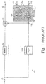
- the decoder 100 shown in Figure 1 has an input 112 for receiving a composite colour video signal in the form of a PAL signal to which is connected a chrominance subcarrier filter 120.
- the filter 120 is a frequency selective filter which selects the frequencies which contain predominantly chrominance rather than luminance information.
- a subtracter 114 is connected to receive the output of the filter 120 at its inverting input, and the PAL input signal, after passing through a compensating delay 116 which compensates for the delay in the filter 120, at its non-inverting input.
- the output 118 of the subtracter 116 constitutes the luminance signal and the output 122 of the filter 120 constitutes the decoded composite chrominance signal.
- This latter signal is then demodulated in a demodulator 124 in one of a number of possible known ways.
- the decoded composite chrominance signal is applied to two multipliers 126, 128 which receive signals at colour subcarrier frequency.
- the two signals are in phase quadrature, with one multiplier receiving an in-phase signal and the other multiplier receiving a quadrature-phase signal, the phase of which is inverted on alternate lines in accordance with the PAL system.
- the multiplier outputs are then low-pass filtered by low-pass filters 130 to provide the U and V output signals 132 and 134.
- the PAL signal is filtered in the filter 120 with the intention of isolating the modulated chrominance. This is then subtracted from the PAL signal in the subtracter 114 to give “clean" luminance, and demodulated to give “clean” colour components.
- the chrominance subcarrier filter 120 shown in Figure 1 is a horizontal band-pass filter centred on subcarrier frequency f SC .
- f SC subcarrier frequency
- Figure 2 illustrates an embodiment of the present invention in which the chrominance selective filter 120 of Figure 1 is replaced by a chrominance selective filter 20 embodying the present invention. Except for the chrominance filter, the circuit of Figure 2 is the same as Figure 1.
- the PAL decoder 10 of Figure 2 has an input 12 for receiving a composite PAL signal to which is connected a chrominance subcarrier filter 20, the construction of which is described below.
- a subtracter 14 is connected to receive the output of the filter 20 at its inverting input, and the PAL input signal, after passing through a compensating delay 16 which compensates for the delay in the filter 20, at its non-inverting input.
- the output 18 of the subtracter 16 constitutes the luminance signal and the output 22 of the filter 20 constitutes the decoded composite chrominance signal.
- this latter signal is then demodulated in a demodulator 24 in one of a number of possible known ways.
- the decoded composite chrominance signal is applied to two multipliers 26, 28 which receive signals at colour subcarrier frequency.
- the two signals are in phase quadrature, with one multiplier receiving an in-phase signal and the other multiplier receiving a quadrature-phase signal, the phase of which is inverted on alternate lines in accordance with the PAL system.
- the multiplier outputs are then low-pass filtered by low-pass filters 30 to provide the U and V output signals 32 and 34.
- the filter 20 embodying the invention and shown in Figure 2 filters the PAL signal in the Fourier transform domain.
- the filtering is effected by a Fourier transform domain filter circuit 40, as described below.
- the filter 20 operates with digital signals.
- the filter 20 has an input 42 connected to the input 12 of the PAL decoder 10 to receive a digital composite chrominance signal.
- To the input 42 is connected a circuit 44 which arranges the incoming data into blocks.
- a multiplier 46 is connected to the output of the data arranging circuit 44 and receives a window signal at an input 48.
- the multiplier is arranged to reduce the effect of black edges.
- the output of the multiplier 46 is then applied to a Fourier transform circuit 50, conveniently implemented as a fast Fourier transform or FFT circuit.
- the transformed signal from the Fourier transform circuit 50 is then applied to the transform domain filter circuit 40.
- the operation of the transform domain filter circuit 40 is described below.
- the output of the transform domain filter circuit 40 is then reverse processed and is applied to an inverse Fourier transform circuit 52 also conveniently implemented as an FFT, a second multiplier 54 receiving a window signal at an input 56, and a data arranging circuit 58 which rearranges the data from blocks back into a sequence corresponding to that received at the input 42.
- the (forward) Fourier transform and the inverse Fourier transform could, in principle, be rearranged.
- the output 22 of the data arranging circuit 58 constitutes the output of the filter 20.
- the circuit of Figure 2 requires the PAL signal to be in digital form or at least to be sampled.
- a good choice of sampling frequency is four times the colour subcarrier frequency f SC , viz. 4 f SC .
- the incoming PAL signal is firstly rearranged into 2 or 3 dimensional blocks in the data arranging circuit 44.
- the blocks may have some degree of overlap if desired.
- the samples are then multiplied in the multiplier 46 by a window function received at input 48, to reduce the effects of block edges, before being transformed into "frequency space” by a discrete Fourier transform applied to each block by the Fourier transform circuit 50.
- a Fourier transform is an example of a time domain to frequency domain transform.
- the transform domain filter 40 modifies some or all of the samples in a block, before it is converted back to "signal space" by an inverse Fourier transform in the inverse Fourier transform circuit 52.
- the samples After multiplying by the inverse of the window function in the multiplier 54, the samples are put back into the correct time order in the data arranging circuit 58. If the blocks have overlap, then some form of averaging or "cross-fading" may be used to combine samples from adjacent blocks.
- the signal may be separated in multi-dimensional frequency components in other ways.
- 2-D or 3-D filters may be used, or one-dimensional filters may be cascaded to achieve the same effect.
- the signal is separated into a plurality of multi-dimensional frequency components before being filtered by the transform domain filter 40.
- successive fields can be vertically displaced, the displacement increasing or decreasing at one picture line per field interval. This displacement may be reset to zero at the start of each block. An opposite displacement is applied after the inverse Fourier transform.
- Figure 3 is a diagram illustrating the horizontal-vertical spectrum of a PAL signal, more particularly it represents the 2-D Fourier transform of one field of a 4 f sc sampled PAL signal.
- the dotted grid lines represent the boundaries between Fourier transform samples, assuming a block size of 16 x 16 samples. The following specific points may be seen on the Figure:
- the modulated U and V signals are not completely symmetric about their subcarriers, as the composite PAL signal is usually low-pass filtered with a cut frequency of about 5.5 MHz.
- the Fourier transform domain signal can be filtered by differentially changing the amplitudes of some of the frequency components.
- the phases should however not be altered.
- each sample has just one mirror, regardless of which subcarrier is chosen. Accordingly the same result is achieved by mirroring about the V subcarrier.
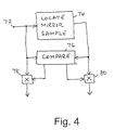
- Figure 4 shows in diagrammatic form a circuit 70 for determining the smaller of the two subcarriers and replacing the larger amplitude of the two by the smaller amplitude, in accordance with the method illustrated in Figure 3.
- the phase is not however changed.
- a component frequency is received at an input 72 and a circuit 74 locates the component which is at the mirror image position about the subcarriers.
- the values of the amplitudes of these two components is compared in a circuit 76 which determines which of the two is the smaller and the ratio of the amplitudes of the two components. It provides two outputs to two respective multipliers 78, 80, associated with the two components respectively.
- the output to the one of the multipliers associated with the smaller of the two components is a unity multiplying factor.
- the circuit 70 as with other circuits described, may be implemented in software, in which case the figure should be regarded as a flowchart rather than a hardware block diagram.
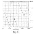
- Figure 5 shows a vertical-temporal slice through the 3-D spectrum of a PAL signal. Note that the slice is at a horizontal frequency of + f SC ; a slice at - f SC would look similar but the locations of the U and V subcarriers would be swapped.
- each U and V subcarrier in Figure 5 is its own reflection in any of the subcarriers.
- Energy at these frequencies will be demodulated as colour with a 25 Hz component - this might be a genuine signal, but is more likely to be cross-colour.
- a variation of the decoder design is to force these samples to zero, so they will always be interpreted as luminance.
- X is an arbitrary frequency
- X' is its mirror about the U carrier at (+72 c/aph, +18.75 Hz). Because the PAL signal is interlaced, every Fourier sample is repeated at a distance of ( ⁇ 288 c/aph, ⁇ 25 Hz) so X and X' each appear twice, as do the U and V subcarriers. As before, X' is also the mirror of X about all the other carriers. To keep the diagram simple, half of the arrows that could be drawn have been omitted, and thus only half are shown.
- the preferred block size to be set by the data arranging circuit 44 of Figure 2 will now be considered.
- One option is to set the block size by requiring a Fourier sample to be centred on a colour subcarrier.
- the PAL signal is sampled at 4 f SC , so the minimum horizontal block size is 4.
- the vertical sampling frequency is 288 c/aph, and subcarrier is at 72 c/aph, so the block size is 4 field lines.
- the vertical sampling frequency is 576 c/aph, so the block size is 8 picture lines.
- the temporal block size, for a 3-D filter is 8 fields, as the temporal sampling frequency is 50 Hz, and subcarrier is at 6.25 Hz (and 18.75 Hz).
- the method also works if the boundary between blocks is centred on a subcarrier instead since this arrangement is also symmetric. In this case we can have a 3-D version with blocks as small as 4 samples x 2 field lines x 2 fields with the fields displaced as described above.
- the upper limit to the block size is set by the picture dimensions (a 4 f SC sampled PAL frame has 576 lines of 945 samples).
- the decoded picture quality degrades as the blocks get larger than about 64 samples or picture lines. This may be because large blocks cover a larger area of picture, so are more likely to encompass different picture material with a wide range of frequencies.
- a block size of 16 samples x 32 picture lines x 8 fields provides good results.
- a range of block sizes between 8 samples x 16 picture lines x 4 fields to 32 samples x 64 picture lines x 16 fields may be considered.
- window function in filters of the kind illustrated by the multipliers 46, 54 in Figure 2.
- a raised cosine window with completely overlapping blocks may be employed. This has the advantage that no inverse windowing is required, as overlapping blocks are simply added together. Windowing in the temporal dimension, using non-overlapping blocks, may give a useful saving in processing and storage, at the expense of a small reduction in decoded picture quality.
- Other window functions could be used, and the block overlap need not be 100%.
Landscapes
- Engineering & Computer Science (AREA)
- Multimedia (AREA)
- Signal Processing (AREA)
- Processing Of Color Television Signals (AREA)
- Color Television Systems (AREA)
Abstract
Description
(-f SC, -72 c/aph) and
(+f SC, -72 c/aph) and (-f SC, +72 c/aph).
Claims (19)
- A method of filtering a sampled composite colour video signal to extract the composite chrominance component therefrom, the method comprising the steps of:separating the signal into a plurality of multi-dimensional frequency components;differentially changing the amplitudes of some of the frequency components to select frequency components at least predominantly representing the composite chrominance component; andcombining the resultant frequency components to provide a sampled output signal.
- A method according to claim 1, in which the changing step comprises:comparing components which are located at mirror images about the colour subcarrier in frequency space;setting the amplitude of the larger of the compared components to that of the smaller.
- A method according to claim 2, in which the frequency space is a three dimensional frequency space (horizontal-vertical-temporal).
- A method according to claim 2, in which the frequency space is a two dimensional frequency space.
- A method according to claim 1 in which the changing step comprises:comparing components which are located at mirror images about the colour subcarrier in frequency space;determining the ratio of amplitudes of the components;setting both components substantially to zero if one is less than a predetermined proportion of the other.
- A method according to claim 1, in which the separating step comprises subjecting the sampled composite colour video signal to a time domain to frequency domain transformation, and the combining step comprises subjecting the resultant frequency components to a frequency domain to time domain transformation.
- A method according to claim 6, in which the time domain to frequency domain and frequency domain to time domain transformations comprise a Fourier transform and an inverse Fourier transform.
- A method according to claim 6 or 7, further comprising the steps of:prior to the time domain to frequency domain transformation, arranging the samples of the sampled composite colour video signals into blocks; andafter the frequency domain to time domain transformation, re-arranging the samples back into sequential form.
- A method according to claim 8, in which the blocks are three dimensional blocks of a size between 8 samples x 16 picture lines x 4 fields and 32 samples x 64 picture lines x 16 fields.
- A method according to claim 8 or 9, in which the blocks overlap.
- A method according to claim 8, 9 or 10, further comprising between the arranging step and the time domain to frequency domain transformation, applying a windowing function to block edges.
- A method according to claim 11, in which the windowing function is a raised cosine function.
- A method according to any of claims 1 to 12, in which the composite colour video signal is a PAL signal.
- A method according to claim 13, in which the composite colour video signal is sampled at four times the colour subcarrier frequency.
- A method according to any preceding claim, in which the composite colour video signal is an interlaced signal, the method further comprising the step of inserting lines of zero samples so as to make an orthogonal sampling structure prior to the time domain to frequency domain transformation.
- Apparatus for filtering a sampled composite colour video signal to extract the composite chrominance component therefrom, comprising:means for separating the signal into a plurality of multi-dimensional frequency components;means for differentially changing the amplitudes of some of the frequency components to select frequency components at least predominantly representing the composite chrominance component; andmeans for combining the resultant frequency components to provide a sampled output signal.
- A composite colour video signal decoder, comprising:wherein the chrominace filter comprises apparatus in accordance with claim 16.an input for receiving a sampled composite colour video signal;a subtracter having its non-inverting input coupled to the input; anda chrominance filter coupled to the input and having its output coupled to the inverting input of the subtracter;
- A method of filtering a sampled composite colour video signal to extract the composite chrominance component therefrom, substantially as herein described with reference to Figure 2 et seq. of the drawings.
- Apparatus for filtering a sampled composite colour video signal to extract the composite chrominance component therefrom, substantially as herein described with reference to Figure 2 et seq. of the drawings.
Applications Claiming Priority (2)
| Application Number | Priority Date | Filing Date | Title |
|---|---|---|---|
| GB0017903 | 2000-07-20 | ||
| GB0017903A GB0017903D0 (en) | 2000-07-20 | 2000-07-20 | Improvements relating to chrominance selective filtering for use in colour video signal decoding |
Publications (3)
| Publication Number | Publication Date |
|---|---|
| EP1175102A2 true EP1175102A2 (en) | 2002-01-23 |
| EP1175102A3 EP1175102A3 (en) | 2004-06-30 |
| EP1175102B1 EP1175102B1 (en) | 2011-04-13 |
Family
ID=9896068
Family Applications (1)
| Application Number | Title | Priority Date | Filing Date |
|---|---|---|---|
| EP20010306255 Expired - Lifetime EP1175102B1 (en) | 2000-07-20 | 2001-07-20 | Improvements relating to chrominance selective filtering for use in colour video signal decoding |
Country Status (3)
| Country | Link |
|---|---|
| EP (1) | EP1175102B1 (en) |
| DE (1) | DE60144413D1 (en) |
| GB (2) | GB0017903D0 (en) |
Cited By (1)
| Publication number | Priority date | Publication date | Assignee | Title |
|---|---|---|---|---|
| WO2004057877A3 (en) * | 2002-12-20 | 2004-08-19 | Snell & Wilcox Ltd | Improved composite decoding |
Family Cites Families (2)
| Publication number | Priority date | Publication date | Assignee | Title |
|---|---|---|---|---|
| JPS6376596A (en) * | 1986-09-19 | 1988-04-06 | Hitachi Ltd | TV signal processing circuit |
| DE4423226C1 (en) * | 1994-07-01 | 1995-08-24 | Harris Corp | Digital decoding composite video, blanking and synchronisation signals |
-
2000
- 2000-07-20 GB GB0017903A patent/GB0017903D0/en not_active Ceased
-
2001
- 2001-07-20 GB GB0117744A patent/GB2365247B/en not_active Expired - Fee Related
- 2001-07-20 DE DE60144413T patent/DE60144413D1/en not_active Expired - Lifetime
- 2001-07-20 EP EP20010306255 patent/EP1175102B1/en not_active Expired - Lifetime
Cited By (5)
| Publication number | Priority date | Publication date | Assignee | Title |
|---|---|---|---|---|
| WO2004057877A3 (en) * | 2002-12-20 | 2004-08-19 | Snell & Wilcox Ltd | Improved composite decoding |
| JP2006511136A (en) * | 2002-12-20 | 2006-03-30 | スネル アンド ウィルコックス リミテッド | Improved composite signal decoding method |
| JP2009290900A (en) * | 2002-12-20 | 2009-12-10 | Snell Ltd | Improved composite signal decoding method |
| US7872689B2 (en) | 2002-12-20 | 2011-01-18 | Snell Limited | System and method for improved composite decoding |
| US8279350B2 (en) | 2002-12-20 | 2012-10-02 | Snell Limited | System and method for improved composite decoding |
Also Published As
| Publication number | Publication date |
|---|---|
| GB2365247B (en) | 2004-09-29 |
| DE60144413D1 (en) | 2011-05-26 |
| GB2365247A (en) | 2002-02-13 |
| EP1175102B1 (en) | 2011-04-13 |
| GB0117744D0 (en) | 2001-09-12 |
| GB0017903D0 (en) | 2000-09-06 |
| EP1175102A3 (en) | 2004-06-30 |
Similar Documents
| Publication | Publication Date | Title |
|---|---|---|
| KR920010901B1 (en) | TV-type signal processing and receiving device | |
| US4551753A (en) | Picture signal processing system including spatio-temporal filter | |
| KR100188832B1 (en) | Transmitting auxiliary information in a television signal | |
| US6175389B1 (en) | Comb filtered signal separation | |
| US4335395A (en) | Standards conversion of color television signals | |
| US7027102B2 (en) | Software decoding of composite video without a phase-locked loop | |
| EP0638220B1 (en) | Video signal coding | |
| KR930002142B1 (en) | Multiple signal transmitter and multiple signal receiver | |
| EP0436549B1 (en) | System for combining and separating components of a video signal | |
| US20040017507A1 (en) | Motion compensation of images | |
| US6052157A (en) | System and method for separating chrominance and luminance components of a color television system | |
| EP0690632B1 (en) | Digital decoder for video signals and video signal digital decoding method | |
| US4829367A (en) | Apparatus and method for encoding and decoding a NTSC color video signal | |
| EP1175102B1 (en) | Improvements relating to chrominance selective filtering for use in colour video signal decoding | |
| US5561473A (en) | Contour correction signal generating circuit | |
| FI87961C (en) | Television signal encoded with extra vertical temporal information | |
| EP0218241A2 (en) | Bi-dimensional comb filter | |
| US5227879A (en) | Apparatus for transmitting an extended definition TV signal having compatibility with a conventional TV system | |
| EP0489713A2 (en) | Spatial-temporal frequency interleaved processing of a television signal | |
| KR100510471B1 (en) | Apparatus for separating luminance and color signal using adaptive comb filter | |
| JP4712392B2 (en) | Improved composite signal decoding method | |
| FI88349C (en) | Signal process system for wide-screen television with uniform image resolution for center and side bands | |
| JPH0338991A (en) | Luminance signal/color signal separation circuit | |
| JP2685542B2 (en) | Chroma signal processing circuit | |
| Perlman et al. | An adaptive luma-chroma separator circuit for PAL and NTSC TV signals |
Legal Events
| Date | Code | Title | Description |
|---|---|---|---|
| PUAI | Public reference made under article 153(3) epc to a published international application that has entered the european phase |
Free format text: ORIGINAL CODE: 0009012 |
|
| AK | Designated contracting states |
Kind code of ref document: A2 Designated state(s): AT BE CH CY DE DK ES FI FR GB GR IE IT LI LU MC NL PT SE TR |
|
| AX | Request for extension of the european patent |
Free format text: AL;LT;LV;MK;RO;SI |
|
| PUAL | Search report despatched |
Free format text: ORIGINAL CODE: 0009013 |
|
| AK | Designated contracting states |
Kind code of ref document: A3 Designated state(s): AT BE CH CY DE DK ES FI FR GB GR IE IT LI LU MC NL PT SE TR |
|
| AX | Request for extension of the european patent |
Extension state: AL LT LV MK RO SI |
|
| 17P | Request for examination filed |
Effective date: 20041229 |
|
| AKX | Designation fees paid |
Designated state(s): BE DE FR GB IT |
|
| 17Q | First examination report despatched |
Effective date: 20050725 |
|
| GRAP | Despatch of communication of intention to grant a patent |
Free format text: ORIGINAL CODE: EPIDOSNIGR1 |
|
| GRAS | Grant fee paid |
Free format text: ORIGINAL CODE: EPIDOSNIGR3 |
|
| GRAA | (expected) grant |
Free format text: ORIGINAL CODE: 0009210 |
|
| AK | Designated contracting states |
Kind code of ref document: B1 Designated state(s): BE DE FR GB IT |
|
| REG | Reference to a national code |
Ref country code: GB Ref legal event code: FG4D |
|
| REF | Corresponds to: |
Ref document number: 60144413 Country of ref document: DE Date of ref document: 20110526 Kind code of ref document: P |
|
| REG | Reference to a national code |
Ref country code: DE Ref legal event code: R096 Ref document number: 60144413 Country of ref document: DE Effective date: 20110526 |
|
| PLBE | No opposition filed within time limit |
Free format text: ORIGINAL CODE: 0009261 |
|
| STAA | Information on the status of an ep patent application or granted ep patent |
Free format text: STATUS: NO OPPOSITION FILED WITHIN TIME LIMIT |
|
| 26N | No opposition filed |
Effective date: 20120116 |
|
| REG | Reference to a national code |
Ref country code: DE Ref legal event code: R097 Ref document number: 60144413 Country of ref document: DE Effective date: 20120116 |
|
| PGFP | Annual fee paid to national office [announced via postgrant information from national office to epo] |
Ref country code: DE Payment date: 20130717 Year of fee payment: 13 Ref country code: BE Payment date: 20130712 Year of fee payment: 13 |
|
| PGFP | Annual fee paid to national office [announced via postgrant information from national office to epo] |
Ref country code: FR Payment date: 20130724 Year of fee payment: 13 Ref country code: GB Payment date: 20130717 Year of fee payment: 13 |
|
| PGFP | Annual fee paid to national office [announced via postgrant information from national office to epo] |
Ref country code: IT Payment date: 20130716 Year of fee payment: 13 |
|
| REG | Reference to a national code |
Ref country code: DE Ref legal event code: R119 Ref document number: 60144413 Country of ref document: DE |
|
| GBPC | Gb: european patent ceased through non-payment of renewal fee |
Effective date: 20140720 |
|
| REG | Reference to a national code |
Ref country code: FR Ref legal event code: ST Effective date: 20150331 |
|
| PG25 | Lapsed in a contracting state [announced via postgrant information from national office to epo] |
Ref country code: IT Free format text: LAPSE BECAUSE OF NON-PAYMENT OF DUE FEES Effective date: 20140720 Ref country code: DE Free format text: LAPSE BECAUSE OF NON-PAYMENT OF DUE FEES Effective date: 20150203 |
|
| REG | Reference to a national code |
Ref country code: DE Ref legal event code: R119 Ref document number: 60144413 Country of ref document: DE Effective date: 20150203 |
|
| PG25 | Lapsed in a contracting state [announced via postgrant information from national office to epo] |
Ref country code: GB Free format text: LAPSE BECAUSE OF NON-PAYMENT OF DUE FEES Effective date: 20140720 Ref country code: FR Free format text: LAPSE BECAUSE OF NON-PAYMENT OF DUE FEES Effective date: 20140731 |
|
| PG25 | Lapsed in a contracting state [announced via postgrant information from national office to epo] |
Ref country code: BE Free format text: LAPSE BECAUSE OF NON-PAYMENT OF DUE FEES Effective date: 20140731 |