EP1175054A1 - Receiver - Google Patents
Receiver Download PDFInfo
- Publication number
- EP1175054A1 EP1175054A1 EP01906176A EP01906176A EP1175054A1 EP 1175054 A1 EP1175054 A1 EP 1175054A1 EP 01906176 A EP01906176 A EP 01906176A EP 01906176 A EP01906176 A EP 01906176A EP 1175054 A1 EP1175054 A1 EP 1175054A1
- Authority
- EP
- European Patent Office
- Prior art keywords
- signal
- quantizing error
- error reduction
- reduction
- bit number
- Prior art date
- Legal status (The legal status is an assumption and is not a legal conclusion. Google has not performed a legal analysis and makes no representation as to the accuracy of the status listed.)
- Withdrawn
Links
Images




Classifications
-
- H—ELECTRICITY
- H03—ELECTRONIC CIRCUITRY
- H03D—DEMODULATION OR TRANSFERENCE OF MODULATION FROM ONE CARRIER TO ANOTHER
- H03D3/00—Demodulation of angle-, frequency- or phase- modulated oscillations
- H03D3/02—Demodulation of angle-, frequency- or phase- modulated oscillations by detecting phase difference between two signals obtained from input signal
- H03D3/06—Demodulation of angle-, frequency- or phase- modulated oscillations by detecting phase difference between two signals obtained from input signal by combining signals additively or in product demodulators
- H03D3/12—Demodulation of angle-, frequency- or phase- modulated oscillations by detecting phase difference between two signals obtained from input signal by combining signals additively or in product demodulators by means of discharge tubes having more than two electrodes
Definitions
- the present invention relates to a receiver used for various communication systems including a mobile communication system and a satellite communication system.
- a receiver used for various communication systems has an A/D converter for converting an analog receiving signal into a digital signal with the advance of recent digitizing technology.
- the more a bit number (count) of the converted digital signal increases the more a resolution improves.
- a circuit scale of receiver becomes large, and further, power consumption is increased.
- the bit number of the converted digital signal is reduced, and thereby, it is possible to achieve a reduction of the circuit scale and power consumption.
- the bit number is reduced, and thereby, a quantizing error of the digital signal increases; as a result, a problem arises such that signal detection accuracy is deteriorated.
- Fig. 8 is a block diagram showing a configuration of the A/D converter circuit.
- an overlapping signal generator circuit 102 generates a constant amplitude overlapping signal S102 having a frequency, which is less than 1/2 times of a sampling pulse S105 generated by a sampling pulse generator circuit 105, and is higher than the maximum frequency of an analog input signal S101.
- An adder 103 adds the overlapping signal S102 to the analog input signal S101, and then, inputs an added signal S103 to an A/D converter 104.
- the A/D converter 104 converts the signal S103 into a digital signal S104 based on the sampling pulse S105, and then, outputs it.
- a low-pass filter 106 outputs a digital signal S106 attenuating the overlapping signal S102 component of the input digital signal S104.
- the overlapping signal S102 is added to the A/D-converted analog input signal, and thereby, a quantizing error is reduced in the A/D conversion.
- the overlapping signal S102 input to the adder 103 of the above A/D converter circuit is an analog signal; for this reason, there is a problem that each circuit scale of the overlapping signal generator circuit 102 and the adder 103 becomes large. As a result, it is impossible to achieve a reduction of circuit scale and power consumption in the entirety of receiver.
- an object of the present invention to provide a receiver, which can output a digital signal reducing a quantizing error even if a bit number of digital signal generated by an A/D conversion is modified, and can reduce a circuit scale and power consumption by modifying the bit number, in particular, reducing the bit number.
- the present invention provides a receiver which comprises at least one A/D converter which converts received analog signal into a digital signal; a reduction signal generator which generates a random noise quantizing error reduction signal for reducing a quantizing error of the digital signal converted by the A/D converter; at least one adder which adds the digital signal and the quantizing error reduction signal generated by the reduction signal generator; at least one bit number modifier which modifies a bit number of an addition signal added by the adder; and at least one low-pass filter which removes a quantizing error reduction signal included in the digital signal having a bit number modified by the bit number modifier.
- the adder adds the digital signal output from the A/D converter and the quantizing error reduction signal output from the reduction signal generator, and the bit number modifier modifies the bit number, for example, reduces the bit number.
- the quantizing error reduction signal is added to the digital signal, and thereby, a correlation is offset between the receiving digital signal and quantizing error generated by the modification of bit number. Therefore, it is possible to prevent a signal deterioration due to quantizing generated by the modification of bit number. Further, the added quantizing error reduction signal is removed by the low-pass filter.
- the present invention provides a receiver which comprises at least one A/D converter which converts a spread spectrum received analog signal into a digital signal; a reduction signal generator which generates a random noise quantizing error reduction signal for reducing a quantizing error of the digital signal converted by the A/D converter; at least one adder which adds the digital signal and the quantizing error reduction signal generated by the reduction signal generator; at least one bit number modifier which modifies a bit number of an addition signal added by the adder; at least one de-spread unit which de-spreads the digital signal having a bit number modified by the bit number modifier; and at least one integral processing unit which integrates the digital signal de-spread by the de-spread unit.
- the adder adds the digital signal output from the A/D converter and the quantizing error reduction signal output from the reduction signal generator, and the bit number modifier modifies the bit number, for example, reduces the bit number.
- the quantizing error reduction signal is added to the digital signal, and thereby, a correlation is offset between the receiving digital signal and quantizing error generated by the modification of bit number. Therefore, it is possible to prevent a signal deterioration due to quantizing generated by the modification of bit number. Further, the added quantizing error reduction signal is securely removed by integral equalization effect by the de-spread unit and integral processing unit.
- the quantizing error reduction signal gene rated by the reduction signal generator is a triangular wave signal.
- the quantizing error reduction signal generated by the reduction signal generator is a triangular wave signal, and the triangular wave signal has a uniform distribution. Therefore, it is possible to interpolate and restore a signal component lost by the reduction of bit number. Further, the frequency characteristic of the triangular wave signal exists in a high frequency band, so that the quantizing error reduction signal can be readily removed. Furthermore, the triangular wave signal can be generated by a simple configuration.
- the quantizing error reduction signal generated by the reduction signal generator is a signal having an orthogonal code having an orthogonal relation with a spreading code used when the de-spread unit de-spreads an input digital signal.
- the quantizing error reduction signal generated by the reduction signal generator is a signal having an orthogonal code, which has an orthogonal relation with a spreading code used in the case of de-spread a digital signal input to the de-spread unit.
- the quantizing error reduction signal is offset by de-spread of the de-spread unit and integral processing of the integral processing unit so that the quantizing error reduction signal can be readily removed.
- the quantizing error reduction signal generated by the reduction signal generator is a signal having a high frequency band as compared with a frequency band of the receiving analog signal.
- the quantizing error reduction signal generated by the reduction signal generator is a signal having a high frequency band as compared with a frequency band of the digital signal, and the receiving digital signal and the quantizing error reduction signal are separated on the frequency axis.
- the quantizing error reduction signal generated by the reduction signal generator is a rectangular wave signal having a uniform distribution.
- the quantizing error reduction signal generated by the reduction signal generator is a rectangular wave signal having a uniform distribution. Therefore, it is possible to more accurately interpolate and restore a signal component lost' by the uniform distribution of the rectangular wave signal and the reduction of bit number. Further, the rectangular wave signal is realized by a simple configuration.
- the receiver further comprises at least one matched filter, which is arranged on the pre-stage of the low-pass filter.
- the matched filter is arranged on the pre-stage of the low-pass filter, and only when the matched filter makes an output operation, the low-pass filter is operated. Therefore, the number of operation times of low-pass filter is reduced.
- Fig. 1 is a block diagram showing a configuration of receiver according to a first embodiment of the present invention
- Fig. 2 is a block diagram showing a configuration of receiver according to a second embodiment of the present invention
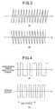
- Fig. 3 is a waveform chart showing a quantizing error reduction signal generated by a receiver according to a third embodiment of the present invention
- Fig. 4 is a waveform chart showing a quantizing error reduction signal generated by a receiver according to a fourth embodiment of the present invention
- Fig. 5 is a waveform chart showing a quantizing error reduction signal generated by a receiver according to a fifth embodiment of the present invention
- Fig. 6 is a waveform chart showing a quantizing error reduction signal generated by a receiver according to a sixth embodiment of the present invention
- Fig. 7 is a block diagram showing a configuration of receiver according to a seventh embodiment of the present invention
- Fig. 8 is a block diagram showing a configuration of conventional A/D converter.
- Fig. 1 is a block diagram showing a configuration of receiver according to a first embodiment of the present invention.
- analog receiving signals I1, Q1 I2 and Q2 orthogonally separated for each branch are input into A/D converters 1-1 to 1-4, and thereafter, are converted into N bit, for example, 16 bit digital signals S1-1 to S1-4, respectively.
- These digital signals S1-1 to S1-4 are input individually into adders 3-1 to 3-4.
- a quantizing error reduction signal generator 2 inputs quantizing error reduction signals S2-1 to S2-4 for reducing a quantizing error with respect to each of the adders 3-1 to 3-4.
- Each of these quantizing error reduction signals S2-1 to S2-4 is a digital random noise signal, for example. Further, these quantizing error reduction signals S2-1 to S2-4 may. be the same signal or different signal.
- the adders 3-1 to 3-4 add the digital signals S1-1 to S1-4 output from the A/D converters 1-1 to 1-4 and the quantizing error reduction signals S2-1 to S2-4, and then, output the added digital signals S3-1 to S3-4 to bit shift circuits 4-1 to 4-4, respectively.
- the bit shift circuits 4-1 to 4-4 reduces each bit number N of the input digital signals S3-1 to S3-4 to a bit number N' (N' ⁇ N). For example, 16-bit digital signals S3-1 to S3-4 are individually reduced to 12-bit digital signal.
- the digital signals S4-1 to S4-4 thus reduced are input to low-pass filters 5-1 and 5-2 for each branch. In other words, for each branch, a 2N'-bit digital signal is input to each of the low-pass filters 5-1 and 5-2.
- the low-pass filters 5-1 and 5-2 restore and output a digital signal before reducing the bit number by the bit shift circuits 4-1 to 4-4 and removing the quantizing error reduction signals S2-1 to S2-4.
- Matched filters 6-1 and 6-2 control each phase of the digital signals output from the low-pass filters 5-1 and 5-2, and then, output it to a demodulation section 7.
- the demodulation section 7 performs demodulation processing with respect to each branch based on a signal output from each of the matched filters 6-1 and 6-2.
- the adders 2-1 to 2-4 the quantizing error reduction signal S2-1 to S2-4 are added to the digital signals S1-1 to S1-4, and thereby, a correlation is offset between the digital signals S1-1 to S1-4 and a quantizing error generated by the reduction of bit number. As a result, signal deterioration by quantizing can be prevented. Further, the bit number is reduced, and thereby, it is possible to prevent a deterioration of signal detection accuracy by the reduction of bit number, and to realize a reduction of circuit scale of the entirety of receiver and a reduction of power consumption.
- the second embodiment of the present invention will be described below. According to the second embodiment, it is possible to effectively reduce a quantizing error generated by the reduction of bit number of a receiver used for a spread spectrum communication system.
- Fig. 2 is a block diagram showing a configuration of receiver according to a second embodiment of the present invention.
- analog receiving signals I11, Q11, I12 and Q12 orthogonally separated and spectrum-spread for each branch are input into A/D converters 1-1 to 1-4, and thereafter, are converted into N-bit, for example, 16-bit digital signals S1-1 to S1-4, respectively.
- These digital signals S1-1 to S1-4 are input into adders 3-1 to 3-4, respectively.
- a quantizing error reduction signal generator 2 inputs quantizing error reduction signals S2-1 to S2-4 for reducing a quantizing error with respect to each of the adders 3-1 to 3-4.
- Each of these quantizing error reduction signals S2-1 to S2-4 is a digital random noise signal, for example. Further, these quantizing error reduction signals S2-1 to S2-4 may be the same signal or different signal.
- the adders 3-1 to 3-4 add the digital signals S1-1 to S1-4 output from the A/D converters 1-1 to 1-4 and the quantizing error reduction signals S2-1 to S2-4, and then, output the added digital signals S3-1 to S3-4 to bit shift circuits 4-1 to 4-4, respectively.
- the bit shift circuits 4-1 to 4-4 reduces each bit number N of the input digital signals S3-1 to S3-4 to a bit number N' (N' ⁇ N). For example, 16-bit digital signals S3-1 to S3-4 are individually reduced to 12-bit digital signal.
- the quantizing error reduction signal S2-1 to S2-4 are added to the digital signals S1-1 to S1-4.
- the reduced digital signals S4-1 to S4-4 are input into de-spread sections 15-1 and 15-2 for each branch. In other words, 2N'-bit digital signals are input individually into the de-spread section 15-1 and 15-2 for each branch.
- the de-spread sections 15-1 and 15-2 multiply the input digital signals by a spreading code such as PN code used in a transmitter side so as to perform de-spread. Subsequently, the integral processing sections 16-1 and 16-2 make a correlation, and then, output the correlation result to a spread spectrum demodulation section 17.
- a quantizing error reduction signal included in the digital signal is removed and equalized by integrating; as a result, it is possible to restore a signal corresponding to the digital signal before reducing the bit number and removing the quantizing error reduction signals S2-1 to S2-4.
- the spread spectrum demodulation section 17 performs a demodulation with respect to each branch based on each signal output from the integral processing sections 16-1 and 16-2.
- This second embodiment relates to a receiver used for spread spectrum communication. Even if there exists a non-observable signal due to the reduction of bit number by the bit shift circuits 4-1 to 4-4, by the adders 2-1 to 2-4, the quantizing error reduction signal S2-1 to S2-4 are added to the digital signals S1-1 to S1-4. By doing so, it is possible to maintain signal detection accuracy before the reduction of bit number. Further, the bit number is reduced, and thereby, it is possible to prevent a deterioration of signal detection accuracy by the reduction of bit number while realizing a reduction of circuit scale of the entirety of receiver and a reduction of power consumption.
- the quantizing error reduction signals S2-1 to S2-4 are a random noise signal.
- the quantizing error reduction signals S2-1 to S2-4 are a triangular wave signal.
- the quantizing error reduction signal generator 2 generates a triangular wave signal as shown in Fig. 3, and inputs the generated signal to each of the adders 3-1 to 3-4.
- Other configuration is the same as the first or second embodiment.
- a triangular waveform as shown in Fig. 3 is generated as a digital signal.
- the triangular wave signal may be a signal such that gradually increasing waveform is repeated as shown in Fig. 3(a), or may be a signal such that a gradually decreasing waveform is repeated as shown in Fig. 3(b).
- the triangular wave signal may be a signal such that a combination of increasing and decreasing wave form is repeated.
- the triangular wave signal is generated by a simple circuit configuration.
- the triangular wave signal is generated by a simple configuration as compared with the case of generating a quantizing error reduction signal such as a random noise signal or the like.
- the triangular wave signal has a feature such that a uniform distribution as compared with a quantizing error reduction signal such as a random noise signal or the like, and a frequency characteristic exists in a high frequency band (range) .
- a quantizing error reduction signal such as a random noise signal or the like
- the reason why the frequency characteristic exists in a high frequency band is because a waveform of the triangular wave is not smooth, and has a high frequency component.
- the triangle wave signal has a uniform distribution. Therefore, it is possible to more securely restore and interpolate a signal component lost by the reduction of bit number. Further, the triangular wave signal exists in a high frequency band, and thereby, it is possible to securely remove a quantizing error reduction signal by the low-pass filters 5-1 and 5-2 of the first embodiment or the integral processing sections 16-1 and 16-2 of the second embodiment.
- the triangular wave signal is used as quantizing error reduction signal. Therefore, the receiver has a more simple circuit configuration as a whole . Further, The triangle wave signal has a uniform distribution. Therefore, it is possible to more securely restore and interpolate a quantizing error. Furthermore, the frequency characteristic exists in a high frequency band, and thereby, it is possible to securely remove a. quantizing error reduction signal.
- the random noise signal has been used as the quantizing error reduction signal
- the triangular wave signal has been used as the quantizing error reduction signal.
- an orthogonal signal having an orthogonal relation to the spread signal used in the de-spread sections 15-1 and 15-2 is used as the quantizing error reduction signals S2-1 to S2-4.
- the fourth embodiment has the same configuration as the above second embodiment exclusive of a configuration of the quantizing error reduction signal generator 2.
- the quantizing error reduction signal generator 2 generates and outputs an orthogonal signal having an orthogonal relation to the spread signal used in the de-spread sections 15-1 and 15-2.
- Fig. 4 (a) is a waveform chart showing one example of a quantizing error reduction signal used in third fourth embodiment.
- the quantizing error reduction signal shown in Fig. 4(a) has an orthogonal relation to a spread signal shown in Fig. 4(b).
- one cycle of the spread signal shown in Fig. 4(b) has a value "-1, 1, -1, 1, -1, 1, -1, 1"
- the quantizing error reduction signal show in Fig. 4 (a) has a value "-1, 1, -1, -1, 1, -1, 1, 1" corresponding one cycle of the spread signal, and an inner product of the spread signal and the quantizing error reduction signal becomes zero. Therefore, the former and the latter have an orthogonal relation.
- the quantizing error reduction signal having the orthogonal relation with the spread signal is offset by de-spread of the de-spread sections 15-1 and 15-2 and integral processing of the integral processing sections 16-1 and 16-2. Therefore, the quantizing error reduction signal can be securely removed.
- the orthogonal relation to the spread signal may be made with respect to one cycle of the spread signal, or a plurality of orthogonal signals having an orthogonal relation to partial signals in one cycle of the spread signal may be connected.
- the orthogonal code (signal) having the orthogonal relation with the spread signal is used as the quantizing error reduction signal. Therefore, it is possible to securely remove the quantizing error reduction signal.
- a signal having a high frequency exceeding the maximum frequency of digital signals S1-1 to S1-4 is used as the quantizing error reduction signal.
- the fifth embodiment has the same configuration as the above first or second embodiment exclusive of a configuration of the quantizing error reduction signal generator 2.
- the quantizing error reduction signal generator 2 generates a signal having a high frequency exceeding the maximum frequency of digital signals S1-1 to S1-4.
- the quantizing error reduction signal generator 2 generates a signal as shown in Fig. 5.
- the quantizing error reduction signal is a signal having a high frequency exceeding the maximum frequency of digital signals S1-1 to S1-4, the digital signals S1-1 to S1-4 and the quantizing error reduction signal is distributed in a state of separating from each other on a frequency axis. Therefore, the quantizing error reduction signal can be removed readily and securely by the low-pass filters 5-1 and 5-2 of the first embodiment or by the integral processing sections 16-1 and 16-2 of the second embodiment.
- the frequency of the quantizing error reduction signal is set to a high frequency exceeding the maximum frequency of digital signals S1-1 to S1-4. Therefore, the digital signals S1-1 to S1-4 and the quantizing error reduction signal are securely separated on the frequency axis . As a result, the quantizing error reduction signal can be removed readily and securely.
- a rectangular wave signal having a uniform distribution is used as the quantizing error reduction signal.
- the sixth embodiment has the same configuration as the above first or second embodiment exclusive of a configuration of the quantizing error reduction signal generator 2.
- the quantizing error reduction signal generator 2 generates a rectangular wave signal having a uniform distribution as shown in Fig. 6.
- the rectangular wave signal shown in Fig. 6 is generated by a simple circuit configuration. Further, the rectangular wave signal shown in Fig. 6 has a uniform distribution. Therefore, it is possible to more accurately restore and interpolate a digital signal lost by the reduction of bit number.
- the rectangular wave signal having a uniform distribution is used as the quantizing error reduction signal. Therefore, the receiver has a more simple circuit configuration as a whole . Further, the rectangular wave signal shown has a uniform distribution. Therefore, it is possible to more securely interpolate and restore a quantizing error.
- the matched filters 6-1 and 6-2 are arranged on the pre-stage of the low-pass filters 5-1 and 5-2 of the first embodiment.
- Fig. 7 is a block diagram showing a configuration of receiver according to a seventh embodiment of the present invention.
- the receiver shown in Fig. 7 has a configuration in which the low-pass filters 5-1 and 5-2 and the matched filters 6-1 and 6-2 are replaced in position.
- Other configuration is the same as the receiver shown in fig. 1.
- the low-pass filters 5-1 and 5-2 have been arranged on the pre-stage of the matched filters 6-1 and 6-2; for this reason, every when the signal is input into the matched filters 6-1 and 6-2, the low-pass filters 5-1 and 5-2 must be operated.
- the low-pass filters 5-1 and 5-2 are arranged on the after-stage of the matched filters 6-1 and 6-2. Therefore, only when these matched filters 6-1 and 6-2 make the output, the low-pass filters 5-1 and 5-2 may be operated. As a result, these low-pass filters 5-1 and 5-2 may perform the necessary and least operation. Therefore, the number of operation times of low-pass filters 5-1 and 5-2 is reduced, and thereby, it is possible to greatly reduce the power consumption of the entire receiver.
- the low-pass filters 5-1 and 5-2 have been arranged on the after-stage of the matched filters 6-1 and 6-2. Therefore, the low-pass filters 5-1 and 5-2 may perform the necessary and least operation, and it is possible to greatly reduce the power consumption of the entire receiver.
- the adder adds the digital signal output from the A/D converter and the quantizing error reduction signal output from the reduction signal generator, and the bit number modifier modifies the bit number, for example, reduce the bit number.
- the quantizing error reduction signal is added to the digital signal, and thereby, a correlation is offset between the receiving digital signal and quantizing error generated by the modification of bit number. Therefore, it is possible to prevent a signal deterioration due to quantizing generated by the modification of bit number.
- the added quantizing error reduction signal is removed by the low-pass filter. Therefore, even if the bit number is reduced, it is possible to prevent a deterioration of signal detection accuracy due to quantizing error.
- even if the bit number is reduced it is possible to maintain signal detection accuracy equal to when the bit number is not reduced, so that therefore, the circuit scale can be made small, and power consumption can be reduced.
- the adder adds the digital signal output from the A/D converter and the quantizing error reduction signal output from the reduction signal generator, and the bit number modifier modifies the bit number, for example, reduces the bit number.
- the quantizing error reduction signal is added to the digital signal, and thereby, a correlation is offset between the receiving digital signal and quantizing error generated by the modification of bit number. Therefore, it is possible to prevent a signal deterioration due to quantizing generated by the modification of bit number. Further, the added quantizing error reduction signal is securely removed by integral equalization effect by the de-spread unit and integral processing unit.
- the quantizing error reduction signal generated by the reduction signal generator is a triangular wave signal, and the triangular wave signal has a uniform distribution. Therefore, it is possible to interpolate and restore a signal component lost by the reduction of bit number. Further, the frequency characteristic of the triangular wave signal exists in a high frequency band, so that the quantizing error reduction signal can be readily removed. Furthermore, the triangular wave signal can be generated by a simple configuration. Therefore, it is possible to prevent a deterioration of signal detection accuracy, and to realize the entire receiver with a simple configuration, so that the circuit scale can be made small, and power consumption can be reduced.
- the quantizing error reduction signal generated by the reduction signal generator is a signal having an orthogonal code, which has an orthogonal relation with a spreading code used in the case of de-spread a digital signal input to the de-spread unit.
- the quantizing error reduction signal is offset by de-spread of the de-spread unit and integral processing of the integral processing unit, so that the quantizing error reduction signal can be readily removed. Therefore, it is possible to securely and readily remove the quantizing error reduction signal.
- the quantizing error reduction signal generated by the reduction signal generator is a signal having a high frequency band as compared with a frequency band of the receiving digital signal, and the receiving digital signal and the quantizing error reduction signal are separated on the frequency axis. Therefore, it. is possible to securely and readily remove the quantizing error reduction signal.
- the quantizing error reduction signal generated by the reduction signal generator is a rectangular wave signal having a uniform distribution. Therefore, it is possible to more accurately interpolate and restore a signal component lost by the uniform distribution of the rectangular wave signal and the reduction of bit number. Further, the rectangular wave signal is realized by a simple configuration. Therefore, it is possible to prevent a deterioration of signal detection accuracy, and to realize the entire receiver with a simple configuration, so that.the circuit scale can be made small, and power consumption can be reduced.
- the matched filter is arranged on the pre-stage of the low-pass filter, and only when the matched filter makes an output operation, thelow-pass filter is operated. Therefore, the number of operation times of low-pass filter is reduced, so that the power consumption of the entire receiver can be reduced.
- the present invention is applicable to a receiver used for various communication systems including a mobile communication system and a satellite communication system. Even if the bit number of digital signal generated by A/D conversion is modified, it is possible to output a digital signal reducing a quantizing error, and the bit number is modified, in particular, the bit number is reduced, and thereby, it is effective to make small the circuit scale and to reduce power consumption.
Landscapes
- Engineering & Computer Science (AREA)
- Power Engineering (AREA)
- Analogue/Digital Conversion (AREA)
- Mobile Radio Communication Systems (AREA)
- Digital Transmission Methods That Use Modulated Carrier Waves (AREA)
- Compression, Expansion, Code Conversion, And Decoders (AREA)
Abstract
The present invention provides a receiver including:
A/D converters (1-1 to 1-4) for converting receiving analog
signals (I1, Q1, I2, Q2) into digital signals; a quantizing
error reduction signal generator (2) for generating a random
noise quantizing error reduction; adders (3-1 to 3-4) for
adding the converted digital signal and the quantizing error
reduction signal; bit shift circuits (4-1 to 4-4) for
reducing a bit number of addition; low-pass filters (5-1,
5-2) for removing a quantizing error reduction signal
included in the digital signal having a reduced bit number;
matched filters (6-1, 6-2); and a demodulation section (7).
Description
The present invention relates to a receiver used for
various communication systems including a mobile
communication system and a satellite communication system.
Conventionally, a receiver used for various
communication systems has an A/D converter for converting
an analog receiving signal into a digital signal with the
advance of recent digitizing technology. In the A/D
conversion, the more a bit number (count) of the converted
digital signal increases, the more a resolution improves.
However, in this case, a circuit scale of receiver becomes
large, and further, power consumption is increased. For
this reason, the bit number of the converted digital signal
is reduced, and thereby, it is possible to achieve a reduction
of the circuit scale and power consumption. However, the
bit number is reduced, and thereby, a quantizing error of
the digital signal increases; as a result, a problem arises
such that signal detection accuracy is deteriorated.
In this case, an A/D converter circuit has been known
such that an overlapping signal is added to the analog
receiving signal so as to reduce a quantizing error in the
A/D conversion (see Japanese Patent Application Laid-Open
No. 8-228152). Fig. 8 is a block diagram showing a
configuration of the A/D converter circuit. In Fig. 8, an
overlapping signal generator circuit 102 generates a
constant amplitude overlapping signal S102 having a
frequency, which is less than 1/2 times of a sampling pulse
S105 generated by a sampling pulse generator circuit 105,
and is higher than the maximum frequency of an analog input
signal S101. An adder 103 adds the overlapping signal S102
to the analog input signal S101, and then, inputs an added
signal S103 to an A/D converter 104. The A/D converter 104
converts the signal S103 into a digital signal S104 based
on the sampling pulse S105, and then, outputs it. A low-pass
filter 106 outputs a digital signal S106 attenuating the
overlapping signal S102 component of the input digital signal
S104.
In the A/D converter circuit, the overlapping signal
S102 is added to the A/D-converted analog input signal, and
thereby, a quantizing error is reduced in the A/D conversion.
However, even if the above A/D converter circuit is
applied to a general receiver, if the bit number of the digital
signal after A/D conversion is reduced, and thereafter,
digital signal processing is performed, it is impossible
to reduce the quantizing error due to the reduction of the
bit number. As a result, a problem arises such that signal
detection accuracy is deteriorated.
Further, the overlapping signal S102 input to the adder
103 of the above A/D converter circuit is an analog signal;
for this reason, there is a problem that each circuit scale
of the overlapping signal generator circuit 102 and the adder
103 becomes large. As a result, it is impossible to achieve
a reduction of circuit scale and power consumption in the
entirety of receiver.
It is, therefore, an object of the present invention
to provide a receiver, which can output a digital signal
reducing a quantizing error even if a bit number of digital
signal generated by an A/D conversion is modified, and can
reduce a circuit scale and power consumption by modifying
the bit number, in particular, reducing the bit number.
In order to achieve the above object, the present
invention provides a receiver which comprises at least one
A/D converter which converts received analog signal into
a digital signal; a reduction signal generator which
generates a random noise quantizing error reduction signal
for reducing a quantizing error of the digital signal
converted by the A/D converter; at least one adder which
adds the digital signal and the quantizing error reduction
signal generated by the reduction signal generator; at least
one bit number modifier which modifies a bit number of an
addition signal added by the adder; and at least one low-pass
filter which removes a quantizing error reduction signal
included in the digital signal having a bit number modified
by the bit number modifier.
According to the above-mentioned invention, the adder
adds the digital signal output from the A/D converter and
the quantizing error reduction signal output from the
reduction signal generator, and the bit number modifier
modifies the bit number, for example, reduces the bit number.
The quantizing error reduction signal is added to the digital
signal, and thereby, a correlation is offset between the
receiving digital signal and quantizing error generated by
the modification of bit number. Therefore, it is possible
to prevent a signal deterioration due to quantizing generated
by the modification of bit number. Further, the added
quantizing error reduction signal is removed by the low-pass
filter.
Furthermore, the present invention provides a receiver
which comprises at least one A/D converter which converts
a spread spectrum received analog signal into a digital
signal; a reduction signal generator which generates a random
noise quantizing error reduction signal for reducing a
quantizing error of the digital signal converted by the A/D
converter; at least one adder which adds the digital signal
and the quantizing error reduction signal generated by the
reduction signal generator; at least one bit number modifier
which modifies a bit number of an addition signal added by
the adder; at least one de-spread unit which de-spreads the
digital signal having a bit number modified by the bit number
modifier; and at least one integral processing unit which
integrates the digital signal de-spread by the de-spread
unit.
According to the above-mentioned invention, even if
the receiving analog signal is a spread spectrum signal,
the adder adds the digital signal output from the A/D
converter and the quantizing error reduction signal output
from the reduction signal generator, and the bit number
modifier modifies the bit number, for example, reduces the
bit number. The quantizing error reduction signal is added
to the digital signal, and thereby, a correlation is offset
between the receiving digital signal and quantizing error
generated by the modification of bit number. Therefore,
it is possible to prevent a signal deterioration due to
quantizing generated by the modification of bit number.
Further, the added quantizing error reduction signal is
securely removed by integral equalization effect by the
de-spread unit and integral processing unit.
Furthermore, in the receiver, the quantizing error
reduction signal gene rated by the reduction signal generator
is a triangular wave signal.
According to the above-mentioned invention, the
quantizing error reduction signal generated by the reduction
signal generator is a triangular wave signal, and the
triangular wave signal has a uniform distribution.
Therefore, it is possible to interpolate and restore a signal
component lost by the reduction of bit number. Further,
the frequency characteristic of the triangular wave signal
exists in a high frequency band, so that the quantizing error
reduction signal can be readily removed. Furthermore, the
triangular wave signal can be generated by a simple
configuration.
Moreover, in the receiver, the quantizing error
reduction signal generated by the reduction signal generator
is a signal having an orthogonal code having an orthogonal
relation with a spreading code used when the de-spread unit
de-spreads an input digital signal.
According to the above-mentioned invention, the
quantizing error reduction signal generated by the reduction
signal generator is a signal having an orthogonal code, which
has an orthogonal relation with a spreading code used in
the case of de-spread a digital signal input to the de-spread
unit. The quantizing error reduction signal is offset by
de-spread of the de-spread unit and integral processing of
the integral processing unit so that the quantizing error
reduction signal can be readily removed.
Moreover, in the receiver, the quantizing error
reduction signal generated by the reduction signal generator
is a signal having a high frequency band as compared with
a frequency band of the receiving analog signal.
According to the above-mentioned invention, the
quantizing error reduction signal generated by the reduction
signal generator is a signal having a high frequency band
as compared with a frequency band of the digital signal,
and the receiving digital signal and the quantizing error
reduction signal are separated on the frequency axis.
Moreover, is the receiver, the quantizing error
reduction signal generated by the reduction signal generator
is a rectangular wave signal having a uniform distribution.
According to the above-mentioned invention, the
quantizing error reduction signal generated by the reduction
signal generator is a rectangular wave signal having a
uniform distribution. Therefore, it is possible to more
accurately interpolate and restore a signal component lost'
by the uniform distribution of the rectangular wave signal
and the reduction of bit number. Further, the rectangular
wave signal is realized by a simple configuration.
Moreover, the receiver further comprises at least one
matched filter, which is arranged on the pre-stage of the
low-pass filter.
According to the above-mentioned invention, the
matched filter is arranged on the pre-stage of the low-pass
filter, and only when the matched filter makes an output
operation, the low-pass filter is operated. Therefore, the
number of operation times of low-pass filter is reduced.
Fig. 1 is a block diagram showing a configuration of
receiver according to a first embodiment of the present
invention; Fig. 2 is a block diagram showing a configuration
of receiver according to a second embodiment of the present
invention; Fig. 3 is a waveform chart showing a quantizing
error reduction signal generated by a receiver according
to a third embodiment of the present invention; Fig. 4 is
a waveform chart showing a quantizing error reduction signal
generated by a receiver according to a fourth embodiment
of the present invention; Fig. 5 is a waveform chart showing
a quantizing error reduction signal generated by a receiver
according to a fifth embodiment of the present invention;
Fig. 6 is a waveform chart showing a quantizing error
reduction signal generated by a receiver according to a sixth
embodiment of the present invention; Fig . 7 is a block diagram
showing a configuration of receiver according to a seventh
embodiment of the present invention; and Fig. 8 is a block
diagram showing a configuration of conventional A/D
converter.
Embodiments of receiver according to the present
invention will be explained in detail below with reference
to the accompanying drawings.
Fig. 1 is a block diagram showing a configuration of
receiver according to a first embodiment of the present
invention. As shown in Fig. 1, analog receiving signals
I1, Q1 I2 and Q2 orthogonally separated for each branch are
input into A/D converters 1-1 to 1-4, and thereafter, are
converted into N bit, for example, 16 bit digital signals
S1-1 to S1-4, respectively. These digital signals S1-1 to
S1-4 are input individually into adders 3-1 to 3-4.
A quantizing error reduction signal generator 2 inputs
quantizing error reduction signals S2-1 to S2-4 for reducing
a quantizing error with respect to each of the adders 3-1
to 3-4. Each of these quantizing error reduction signals
S2-1 to S2-4 is a digital random noise signal, for example.
Further, these quantizing error reduction signals S2-1 to
S2-4 may. be the same signal or different signal.
The adders 3-1 to 3-4 add the digital signals S1-1
to S1-4 output from the A/D converters 1-1 to 1-4 and the
quantizing error reduction signals S2-1 to S2-4, and then,
output the added digital signals S3-1 to S3-4 to bit shift
circuits 4-1 to 4-4, respectively. The bit shift circuits
4-1 to 4-4 reduces each bit number N of the input digital
signals S3-1 to S3-4 to a bit number N' (N'<N). For example,
16-bit digital signals S3-1 to S3-4 are individually reduced
to 12-bit digital signal. The digital signals S4-1 to S4-4
thus reduced are input to low-pass filters 5-1 and 5-2 for
each branch. In other words, for each branch, a 2N'-bit
digital signal is input to each of the low-pass filters 5-1
and 5-2.
The low-pass filters 5-1 and 5-2 restore and output
a digital signal before reducing the bit number by the bit
shift circuits 4-1 to 4-4 and removing the quantizing error
reduction signals S2-1 to S2-4. Matched filters 6-1 and
6-2 control each phase of the digital signals output from
the low-pass filters 5-1 and 5-2, and then, output it to
a demodulation section 7. The demodulation section 7
performs demodulation processing with respect to each branch
based on a signal output from each of the matched filters
6-1 and 6-2.
According to the first embodiment, even if there exists
a non-observable signal due to the reduction of bit number
made by the bit shift circuits 4-1 to 4-4, it is possible
to maintain signal detection accuracy before the reduction
of bit number from the following reason. More specifically,
by the adders 2-1 to 2-4, the quantizing error reduction
signal S2-1 to S2-4 are added to the digital signals S1-1
to S1-4, and thereby, a correlation is offset between the
digital signals S1-1 to S1-4 and a quantizing error generated
by the reduction of bit number. As a result, signal
deterioration by quantizing can be prevented. Further, the
bit number is reduced, and thereby, it is possible to prevent
a deterioration of signal detection accuracy by the reduction
of bit number, and to realize a reduction of circuit scale
of the entirety of receiver and a reduction of power
consumption.
The second embodiment of the present invention will
be described below. According to the second embodiment,
it is possible to effectively reduce a quantizing error
generated by the reduction of bit number of a receiver used
for a spread spectrum communication system.
Fig. 2 is a block diagram showing a configuration of
receiver according to a second embodiment of the present
invention. As shown in Fig. 2, analog receiving signals
I11, Q11, I12 and Q12 orthogonally separated and
spectrum-spread for each branch are input into A/D converters
1-1 to 1-4, and thereafter, are converted into N-bit, for
example, 16-bit digital signals S1-1 to S1-4, respectively.
These digital signals S1-1 to S1-4 are input into adders
3-1 to 3-4, respectively.
A quantizing error reduction signal generator 2 inputs
quantizing error reduction signals S2-1 to S2-4 for reducing
a quantizing error with respect to each of the adders 3-1
to 3-4. Each of these quantizing error reduction signals
S2-1 to S2-4 is a digital random noise signal, for example.
Further, these quantizing error reduction signals S2-1 to
S2-4 may be the same signal or different signal.
The adders 3-1 to 3-4 add the digital signals S1-1
to S1-4 output from the A/D converters 1-1 to 1-4 and the
quantizing error reduction signals S2-1 to S2-4, and then,
output the added digital signals S3-1 to S3-4 to bit shift
circuits 4-1 to 4-4, respectively. The bit shift circuits
4-1 to 4-4 reduces each bit number N of the input digital
signals S3-1 to S3-4 to a bit number N' (N'<N). For example,
16-bit digital signals S3-1 to S3-4 are individually reduced
to 12-bit digital signal. In this case, even if there exists
a non-observable signal due to the reduction of bit number
made by the bit shift circuits 4-1 to 4-4, by the adders
2-1 to 2-4, the quantizing error reduction signal S2-1 to
S2-4 are added to the digital signals S1-1 to S1-4. By doing
so, a correlation is offset between the digital signals S1-1
to S1-4 and a quantizing error generated by the reduction
of bit number; as a result, signal deterioration by
quantizing can be prevented. The reduced digital signals
S4-1 to S4-4 are input into de-spread sections 15-1 and 15-2
for each branch. In other words, 2N'-bit digital signals
are input individually into the de-spread section 15-1 and
15-2 for each branch.
The de-spread sections 15-1 and 15-2 multiply the input
digital signals by a spreading code such as PN code used
in a transmitter side so as to perform de-spread.
Subsequently, the integral processing sections 16-1 and 16-2
make a correlation, and then, output the correlation result
to a spread spectrum demodulation section 17. In the
correlation processing, a quantizing error reduction signal
included in the digital signal is removed and equalized by
integrating; as a result, it is possible to restore a signal
corresponding to the digital signal before reducing the bit
number and removing the quantizing error reduction signals
S2-1 to S2-4. The spread spectrum demodulation section 17
performs a demodulation with respect to each branch based
on each signal output from the integral processing sections
16-1 and 16-2.
This second embodiment relates to a receiver used for
spread spectrum communication. Even if there exists a
non-observable signal due to the reduction of bit number
by the bit shift circuits 4-1 to 4-4, by the adders 2-1 to
2-4, the quantizing error reduction signal S2-1 to S2-4 are
added to the digital signals S1-1 to S1-4. By doing so,
it is possible to maintain signal detection accuracy before
the reduction of bit number. Further, the bit number is
reduced, and thereby, it is possible to prevent a
deterioration of signal detection accuracy by the reduction
of bit number while realizing a reduction of circuit scale
of the entirety of receiver and a reduction of power
consumption.
The third embodiment of the present invention will
be descried below. In the above the first embodiments and
the second embodiment, the quantizing error reduction
signals S2-1 to S2-4 are a random noise signal. In this
third embodiment, the quantizing error reduction signals
S2-1 to S2-4 are a triangular wave signal.
In this third embodiment, the quantizing error
reduction signal generator 2 generates a triangular wave
signal as shown in Fig. 3, and inputs the generated signal
to each of the adders 3-1 to 3-4. Other configuration is
the same as the first or second embodiment. In the triangular
wave signal, a triangular waveform as shown in Fig. 3 is
generated as a digital signal. The triangular wave signal
may be a signal such that gradually increasing waveform is
repeated as shown in Fig. 3(a), or may be a signal such that
a gradually decreasing waveform is repeated as shown in Fig.
3(b). Further, the triangular wave signal may be a signal
such that a combination of increasing and decreasing wave form
is repeated. In this case, the triangular wave signal is
generated by a simple circuit configuration. Thus, the
triangular wave signal is generated by a simple configuration
as compared with the case of generating a quantizing error
reduction signal such as a random noise signal or the like.
The triangular wave signal has a feature such that
a uniform distribution as compared with a quantizing error
reduction signal such as a random noise signal or the like,
and a frequency characteristic exists in a high frequency
band (range) . The reason why the frequency characteristic
exists in a high frequency band is because a waveform of
the triangular wave is not smooth, and has a high frequency
component.
The triangle wave signal has a uniform distribution.
Therefore, it is possible to more securely restore and
interpolate a signal component lost by the reduction of bit
number. Further, the triangular wave signal exists in a
high frequency band, and thereby, it is possible to securely
remove a quantizing error reduction signal by the low-pass
filters 5-1 and 5-2 of the first embodiment or the integral
processing sections 16-1 and 16-2 of the second embodiment.
According to the third embodiment, the triangular wave
signal is used as quantizing error reduction signal.
Therefore, the receiver has a more simple circuit
configuration as a whole . Further, The triangle wave signal
has a uniform distribution. Therefore, it is possible to
more securely restore and interpolate a quantizing error.
Furthermore, the frequency characteristic exists in a high
frequency band, and thereby, it is possible to securely
remove a. quantizing error reduction signal.
The fourth embodiment of the present invention will
be described below. In the above second embodiment, the
random noise signal has been used as the quantizing error
reduction signal, and in the above third embodiment, the
triangular wave signal has been used as the quantizing error
reduction signal. In this fourth embodiment, an orthogonal
signal having an orthogonal relation to the spread signal
used in the de-spread sections 15-1 and 15-2 is used as the
quantizing error reduction signals S2-1 to S2-4.
The fourth embodiment has the same configuration as
the above second embodiment exclusive of a configuration
of the quantizing error reduction signal generator 2. The
quantizing error reduction signal generator 2 generates and
outputs an orthogonal signal having an orthogonal relation
to the spread signal used in the de-spread sections 15-1
and 15-2.
Fig. 4 (a) is a waveform chart showing one example of
a quantizing error reduction signal used in third fourth
embodiment. The quantizing error reduction signal shown
in Fig. 4(a) has an orthogonal relation to a spread signal
shown in Fig. 4(b). For example, one cycle of the spread
signal shown in Fig. 4(b) has a value "-1, 1, -1, 1, -1,
1, -1, 1", the quantizing error reduction signal show in
Fig. 4 (a) has a value "-1, 1, -1, -1, 1, -1, 1, 1" corresponding
one cycle of the spread signal, and an inner product of the
spread signal and the quantizing error reduction signal
becomes zero. Therefore, the former and the latter have
an orthogonal relation.
In this case, the quantizing error reduction signal
having the orthogonal relation with the spread signal is
offset by de-spread of the de-spread sections 15-1 and 15-2
and integral processing of the integral processing sections
16-1 and 16-2. Therefore, the quantizing error reduction
signal can be securely removed. Incidentally, the
orthogonal relation to the spread signal may be made with
respect to one cycle of the spread signal, or a plurality
of orthogonal signals having an orthogonal relation to
partial signals in one cycle of the spread signal may be
connected.
According to the fourth embodiment, the orthogonal
code (signal) having the orthogonal relation with the spread
signal is used as the quantizing error reduction signal.
Therefore, it is possible to securely remove the quantizing
error reduction signal.
The fifth embodiment of the present invention will
be described below. In this fifth embodiment, a signal
having a high frequency exceeding the maximum frequency of
digital signals S1-1 to S1-4 is used as the quantizing error
reduction signal.
The fifth embodiment has the same configuration as
the above first or second embodiment exclusive of a
configuration of the quantizing error reduction signal
generator 2. The quantizing error reduction signal
generator 2 generates a signal having a high frequency
exceeding the maximum frequency of digital signals S1-1 to
S1-4. For example, the quantizing error reduction signal
generator 2 generates a signal as shown in Fig. 5.
When the quantizing error reduction signal is a signal
having a high frequency exceeding the maximum frequency of
digital signals S1-1 to S1-4, the digital signals S1-1 to
S1-4 and the quantizing error reduction signal is distributed
in a state of separating from each other on a frequency axis.
Therefore, the quantizing error reduction signal can be
removed readily and securely by the low-pass filters 5-1
and 5-2 of the first embodiment or by the integral processing
sections 16-1 and 16-2 of the second embodiment.
According to the fifth embodiment, the frequency of
the quantizing error reduction signal is set to a high
frequency exceeding the maximum frequency of digital signals
S1-1 to S1-4. Therefore, the digital signals S1-1 to S1-4
and the quantizing error reduction signal are securely
separated on the frequency axis . As a result, the quantizing
error reduction signal can be removed readily and securely.
The sixth embodiment of the present invention will
be described below. In this sixth embodiment, a rectangular
wave signal having a uniform distribution is used as the
quantizing error reduction signal.
The sixth embodiment has the same configuration as
the above first or second embodiment exclusive of a
configuration of the quantizing error reduction signal
generator 2. The quantizing error reduction signal
generator 2 generates a rectangular wave signal having a
uniform distribution as shown in Fig. 6. The rectangular
wave signal shown in Fig. 6 is generated by a simple circuit
configuration. Further, the rectangular wave signal shown
in Fig. 6 has a uniform distribution. Therefore, it is
possible to more accurately restore and interpolate a digital
signal lost by the reduction of bit number.
According to the sixth embodiment, the rectangular
wave signal having a uniform distribution is used as the
quantizing error reduction signal. Therefore, the receiver
has a more simple circuit configuration as a whole . Further,
the rectangular wave signal shown has a uniform distribution.
Therefore, it is possible to more securely interpolate and
restore a quantizing error.
The seventh embodiment of the present invention will
be described below. In this seventh embodiment, the matched
filters 6-1 and 6-2 are arranged on the pre-stage of the
low-pass filters 5-1 and 5-2 of the first embodiment.
Fig. 7 is a block diagram showing a configuration of
receiver according to a seventh embodiment of the present
invention. The receiver shown in Fig. 7 has a configuration
in which the low-pass filters 5-1 and 5-2 and the matched
filters 6-1 and 6-2 are replaced in position. Other
configuration is the same as the receiver shown in fig. 1.
In the above first embodiment, the low-pass filters
5-1 and 5-2 have been arranged on the pre-stage of the matched
filters 6-1 and 6-2; for this reason, every when the signal
is input into the matched filters 6-1 and 6-2, the low-pass
filters 5-1 and 5-2 must be operated. On the contrary, in
this seventh embodiment, the low-pass filters 5-1 and 5-2
are arranged on the after-stage of the matched filters 6-1
and 6-2. Therefore, only when these matched filters 6-1
and 6-2 make the output, the low-pass filters 5-1 and 5-2
may be operated. As a result, these low-pass filters 5-1
and 5-2 may perform the necessary and least operation.
Therefore, the number of operation times of low-pass filters
5-1 and 5-2 is reduced, and thereby, it is possible to greatly
reduce the power consumption of the entire receiver.
According to the seventh embodiment, the low-pass
filters 5-1 and 5-2 have been arranged on the after-stage
of the matched filters 6-1 and 6-2. Therefore, the low-pass
filters 5-1 and 5-2 may perform the necessary and least
operation, and it is possible to greatly reduce the power
consumption of the entire receiver.
As is evident from the above description, according
to the present invention, the adder adds the digital signal
output from the A/D converter and the quantizing error
reduction signal output from the reduction signal generator,
and the bit number modifier modifies the bit number, for
example, reduce the bit number. The quantizing error
reduction signal is added to the digital signal, and thereby,
a correlation is offset between the receiving digital signal
and quantizing error generated by the modification of bit
number. Therefore, it is possible to prevent a signal
deterioration due to quantizing generated by the
modification of bit number. Further, the added quantizing
error reduction signal is removed by the low-pass filter.
Therefore, even if the bit number is reduced, it is possible
to prevent a deterioration of signal detection accuracy due
to quantizing error. In addition, even if the bit number
is reduced, it is possible to maintain signal detection
accuracy equal to when the bit number is not reduced, so
that therefore, the circuit scale can be made small, and
power consumption can be reduced.
Further, according to the present invention, even if
the receiving analog signal is a spread spectrum signal,
the adder adds the digital signal output from the A/D
converter and the quantizing error reduction signal output
from the reduction signal generator, and the bit number
modifier modifies the bit number, for example, reduces the
bit number. The quantizing error reduction signal is added
to the digital signal, and thereby, a correlation is offset
between the receiving digital signal and quantizing error
generated by the modification of bit number. Therefore,
it is possible to prevent a signal deterioration due to
quantizing generated by the modification of bit number.
Further, the added quantizing error reduction signal is
securely removed by integral equalization effect by the
de-spread unit and integral processing unit. Therefore,
even if the bit number is reduced, it is possible to prevent
a deterioration of signal detection accuracy due to
quantizing error. In addition, even if the bit number is
reduced, it is possible to maintain signal detection accuracy
equal to when the bit number is not reduced, so that the
circuit scale can be made small, and power consumption can
be reduced.
Further, according to the present invention, the
quantizing error reduction signal generated by the reduction
signal generator is a triangular wave signal, and the
triangular wave signal has a uniform distribution.
Therefore, it is possible to interpolate and restore a signal
component lost by the reduction of bit number. Further,
the frequency characteristic of the triangular wave signal
exists in a high frequency band, so that the quantizing error
reduction signal can be readily removed. Furthermore, the
triangular wave signal can be generated by a simple
configuration. Therefore, it is possible to prevent a
deterioration of signal detection accuracy, and to realize
the entire receiver with a simple configuration, so that
the circuit scale can be made small, and power consumption
can be reduced.
Further, according to the present invention, the
quantizing error reduction signal generated by the reduction
signal generator is a signal having an orthogonal code, which
has an orthogonal relation with a spreading code used in
the case of de-spread a digital signal input to the de-spread
unit. The quantizing error reduction signal is offset by
de-spread of the de-spread unit and integral processing of
the integral processing unit, so that the quantizing error
reduction signal can be readily removed. Therefore, it is
possible to securely and readily remove the quantizing error
reduction signal.
Further, according to the present invention, the
quantizing error reduction signal generated by the reduction
signal generator is a signal having a high frequency band
as compared with a frequency band of the receiving digital
signal, and the receiving digital signal and the quantizing
error reduction signal are separated on the frequency axis.
Therefore, it. is possible to securely and readily remove
the quantizing error reduction signal.
Further, according to the present invention, the
quantizing error reduction signal generated by the reduction
signal generator is a rectangular wave signal having a
uniform distribution. Therefore, it is possible to more
accurately interpolate and restore a signal component lost
by the uniform distribution of the rectangular wave signal
and the reduction of bit number. Further, the rectangular
wave signal is realized by a simple configuration.
Therefore, it is possible to prevent a deterioration of
signal detection accuracy, and to realize the entire receiver
with a simple configuration, so that.the circuit scale can
be made small, and power consumption can be reduced.
Further, according to the present invention, the
matched filter is arranged on the pre-stage of the low-pass
filter, and only when the matched filter makes an output
operation, thelow-pass filter is operated. Therefore, the
number of operation times of low-pass filter is reduced,
so that the power consumption of the entire receiver can
be reduced.
As described above, the present invention is
applicable to a receiver used for various communication
systems including a mobile communication system and a
satellite communication system. Even if the bit number of
digital signal generated by A/D conversion is modified, it
is possible to output a digital signal reducing a quantizing
error, and the bit number is modified, in particular, the
bit number is reduced, and thereby, it is effective to make
small the circuit scale and to reduce power consumption.
Claims (10)
- A receiver comprising:at least one A/D converter which converts received analog signal into a digital signal;a reduction signal generator which generates a random noise quantizing error reduction signal for reducing a quantizing error of the digital signal converted by the A/D converter;at least one adder which adds the digital signal and the quantizing error reduction signal generated by the reduction signal generator;at least one bit number modifier which modifies a bit number of an addition signal added by the adder; andat least one low-pass filter which removes a quantizing error reduction signal included in the digital signal having a bit number modified by the bit number modifier.
- The receiver according to claim 1, wherein the quantizing error reduction signal generated by the reduction signal generator is a triangular wave signal.
- The receiver according to claim 1, wherein the quantizing error reduction signal generated by the reduction signal generator is a signal having a high frequency band as compared with a frequency band of the receiving analog signal.
- The receiver according to claim 1, wherein the quantizing error reduction signal generated by the reduction signal generator is a rectangular wave signal having a uniform distribution.
- The receiver according to claim 1, further comprising at least one matched filter, which is arranged on the pre-stage of the low-pass filter.
- A receiver comprising:at least one A/D converter which converts a receiving analog signal into a digital signal;a reduction signal generator which generates a random noise quantizing error reduction signal for reducing a quantizing error of the digital signal converted by the A/D converter;at least one adder which adds the digital signal and the quantizing error reduction signal generated by the reduction signal generator;at least one de-spread unit which de-spreads the digital signal having a bit number modified by the bit number modifier; andat least one integral processing unit which integrates the digital signal inverse infused by the de-spread unit.
- The receiver according to claim 2, wherein the quantizing error reduction signal generated by the reduction 5 signal generator is a triangular wave signal.
- The receiver according to claim 2, wherein the quantizing error reduction signal generated by the reduction signal generator is a signal having an orthogonal code having an orthogonal relation with a spreading code used when the de-spread unit de-spreads the input digital signal.
- The receiver according to claim 2, wherein the quantizing error reduction signal generated by the reduction signal generator is a signal having a high frequency band as compared with a frequency band of the receiving analog signal.
- The receiver according to claim 2, wherein the quantizing error reduction signal generated by the reduction signal generator is a rectangular wave signal having a uniform distribution.
Applications Claiming Priority (3)
| Application Number | Priority Date | Filing Date | Title |
|---|---|---|---|
| JP2000048094 | 2000-02-24 | ||
| JP2000048094A JP2001237902A (en) | 2000-02-24 | 2000-02-24 | Receiving machine |
| PCT/JP2001/001262 WO2001063867A1 (en) | 2000-02-24 | 2001-02-21 | Receiver |
Publications (2)
| Publication Number | Publication Date |
|---|---|
| EP1175054A1 true EP1175054A1 (en) | 2002-01-23 |
| EP1175054A4 EP1175054A4 (en) | 2004-10-27 |
Family
ID=18570232
Family Applications (1)
| Application Number | Title | Priority Date | Filing Date |
|---|---|---|---|
| EP01906176A Withdrawn EP1175054A4 (en) | 2000-02-24 | 2001-02-21 | RECEIVER |
Country Status (5)
| Country | Link |
|---|---|
| US (1) | US20020141504A1 (en) |
| EP (1) | EP1175054A4 (en) |
| JP (1) | JP2001237902A (en) |
| CN (1) | CN1366754A (en) |
| WO (1) | WO2001063867A1 (en) |
Families Citing this family (3)
| Publication number | Priority date | Publication date | Assignee | Title |
|---|---|---|---|---|
| JP3440095B1 (en) | 2002-08-23 | 2003-08-25 | 富士通株式会社 | Data transmission device and data transmission method |
| US7660342B2 (en) * | 2005-05-04 | 2010-02-09 | Stmicroelectronics (Rousset) Sas | Digital receiver device based on an input comparator |
| US8326580B2 (en) * | 2008-01-29 | 2012-12-04 | Qualcomm Incorporated | Sparse sampling of signal innovations |
Family Cites Families (9)
| Publication number | Priority date | Publication date | Assignee | Title |
|---|---|---|---|---|
| EP0256076B1 (en) * | 1986-01-30 | 1990-03-28 | Plessey Overseas Limited | Analogue to digital conversion: method and apparatus therefor |
| JPS63256018A (en) * | 1987-04-13 | 1988-10-24 | Nippon Precision Saakitsutsu Kk | A/d converter |
| JPH01202038A (en) * | 1988-02-08 | 1989-08-15 | Sony Corp | Bit reduction system |
| US4958308A (en) * | 1988-10-21 | 1990-09-18 | Bio-Rad Laboratories, Inc. | Technique for improving the resolution of an A/D converter |
| JP2572141B2 (en) * | 1990-02-08 | 1997-01-16 | 株式会社エイ・ティ・アール光電波通信研究所 | Phased array antenna |
| US5166952A (en) * | 1990-05-24 | 1992-11-24 | Cylink Corporation | Method and apparatus for the reception and demodulation of spread spectrum radio signals |
| JP3684655B2 (en) * | 1996-03-13 | 2005-08-17 | ソニー株式会社 | Digital signal processor |
| JP2970550B2 (en) * | 1996-09-13 | 1999-11-02 | 日本電気株式会社 | Batch demultiplexer |
| JPH11340949A (en) * | 1998-05-21 | 1999-12-10 | Matsushita Electric Ind Co Ltd | CDMA communication device and CDMA communication method |
-
2000
- 2000-02-24 JP JP2000048094A patent/JP2001237902A/en active Pending
-
2001
- 2001-02-21 CN CN01801010A patent/CN1366754A/en active Pending
- 2001-02-21 WO PCT/JP2001/001262 patent/WO2001063867A1/en not_active Ceased
- 2001-02-21 EP EP01906176A patent/EP1175054A4/en not_active Withdrawn
- 2001-02-21 US US09/926,364 patent/US20020141504A1/en not_active Abandoned
Also Published As
| Publication number | Publication date |
|---|---|
| WO2001063867A1 (en) | 2001-08-30 |
| CN1366754A (en) | 2002-08-28 |
| EP1175054A4 (en) | 2004-10-27 |
| JP2001237902A (en) | 2001-08-31 |
| US20020141504A1 (en) | 2002-10-03 |
Similar Documents
| Publication | Publication Date | Title |
|---|---|---|
| US6173003B1 (en) | Dither noise source with notched frequency spectrum | |
| US5010347A (en) | Analog-to-digital converter having an excellent signal-to-noise ratio for small signals | |
| US5075679A (en) | Analog/digital converter configuration with sigma-delta modulators | |
| US6983011B1 (en) | Filter circuit | |
| JPH08181573A (en) | Cascaded integrator | |
| US20070188357A1 (en) | Bi-Quad Digital Filter Configured With A Bit Binary Rate Multiplier | |
| US6285306B1 (en) | Circuits and methods for functional processing of delta modulated pulse density stream | |
| JP2004521568A (en) | Fractional decimation filter using oversampled data | |
| EP1097520A2 (en) | Cdma receiver and method of operation | |
| US4947408A (en) | Digital carrier demodulator employing components working beyond normal limits | |
| EP1175054A1 (en) | Receiver | |
| JP2742519B2 (en) | Differential signal detection matched filter for use in spread spectrum communication systems. | |
| US7068196B2 (en) | Digital signal processing device and digital signal processing method | |
| US20020050937A1 (en) | Method and device for digital-to-analog conversion of a signal | |
| JP2002043965A (en) | Receiver | |
| EP0845866B1 (en) | Signal processors | |
| JPH06244678A (en) | Digital filter circuit | |
| US20080084921A1 (en) | Spectrally shaped pseudo-random noise sequence generator and method thereof | |
| US7385538B2 (en) | Delta sigma modulator with multiple filters | |
| JP3036045B2 (en) | D / A converter | |
| US7166995B2 (en) | Digital power meter apparatus and method for the same | |
| KR20110038991A (en) | Operation Method of Offset Pulse Generator for Peak Reduction in Multicarrier System and Pc-Cfr Device | |
| JP2000224041A (en) | ΔΣ AD converter and receiver | |
| Yan et al. | Design of Multi-Mode Digital Signal Processing Circuit for Digital Transmitters | |
| SU1499508A1 (en) | Arrangement for monitoring communication channel quality |
Legal Events
| Date | Code | Title | Description |
|---|---|---|---|
| PUAI | Public reference made under article 153(3) epc to a published international application that has entered the european phase |
Free format text: ORIGINAL CODE: 0009012 |
|
| 17P | Request for examination filed |
Effective date: 20011011 |
|
| AK | Designated contracting states |
Kind code of ref document: A1 Designated state(s): AT BE CH CY DE DK ES FI FR GB GR IE IT LI LU MC NL PT SE TR |
|
| RBV | Designated contracting states (corrected) |
Designated state(s): DE FI FR GB SE |
|
| A4 | Supplementary search report drawn up and despatched |
Effective date: 20040909 |
|
| STAA | Information on the status of an ep patent application or granted ep patent |
Free format text: STATUS: THE APPLICATION IS DEEMED TO BE WITHDRAWN |
|
| 18D | Application deemed to be withdrawn |
Effective date: 20040830 |