BACKGROUND OF THE INVENTION
1. Field of the Invention
The present invention relates to a WDM transmission
(WDM) system and a transmitter and a receiver therefor.
More particularly, the invention relates to the WDM
transmission that keeps an optical power in an appropriate
level to prevent the transmission of other normal optical
signals from being adversely affected when an optical
signal with specific wavelength is missed.
2. Description of the Related Art
As a digital transmission system in a public
communication network using an optical fiber, a system
is known in which a Synchronous Digital Hierarchy (SDH)
device and the Wavelength Division Multiplexing (WDM)
device are combined. Fig. 3 shows the block diagram of
the combined system. A transmitting station 301 comprises
an SDH device 311, the plural optical transmitters (10l
∼ 10N), an optical multiplexing filter 312, and an optical
output amplifier 313. Optical signals from SDH device
311, the wavelengths of which are in 1.3µ m band, are led
into the corresponding transmitter and transmitter
outputs the optical signal of the 1.55 µm wavelength band
for the WDM transmission. Respective optical signals from
transmitters are multiplexed in the optical multiplexing
filter 312, and multiplexed signal is amplified in the
optical amplifier 313 and output to a transmission line
303.
In a receiving station 302, the WDM signal
transmitted from the transmission line 303 is
de-multiplexed in a de-multiplexed filter 322. One optical
signal de-multiplexed in the filter 322 is led to the
corresponding receiver (20l ∼ 20N). In the receiver, the
inputted optical signal with 1.55 µm wavelength band is
output to the SDH device 323 after the wavelength
converting to the 1.3 µm band.
The optical transmission system as shown in the Fig.
3, some cases will occur that one or more optical signals
input into transmitter disappear due to, for example,
the disconnection of an optical connector or the breaking
of the optical fiber. The output of the receiver coupled
to such signal disappearing input will vanish. Since the
output amplifier 313 or the amplifier inserted into the
optical transmission line 304 operates so as to keep its
optical output power to be constant (Automatic Power
Control), optical signals for not disappearing wavelength
are amplified over to its appropriate level, which lowers
the Signal to Noise Ratio (SNR), or may cause the breakdown
of the receiver (20l∼20N) due to the excessive optical
input power.
Some techniques to overcome problems above mentioned
are known. One is to provide a spare transmitter that
outputs the light with the extra wavelength to the signal
light (Japanese Patent Unexamined Publication No. Hei.
10-322287). When the input signal light disappears at
one transmitter, the extra transmitter will substitute
for such signal disappearing transmitter and the optical
power level of the optical multiplexing filter output
to the transmission line will maintain the predetermined
value.
The other method is to adjust the wavelength of the
light output from the extra transmitter to that of
disappearing signal. The optical output level of the
multiplexing filter will be also constant in this method.
However, alternative explained above needs at least
one extra transmitter and to change the transmitters and
to adjust the wavelength become complicated, which result
in the raising the device.cost.
Another technique is also known in the WDM system
that the information in the transmitting station, which
contains the signal disappearing or the signal
out-synchronizing in some transmitter are transferred
to the receiving station by the extra wavelength not
corresponding to the signal one. In the receiving station,
the optical output of the receiver corresponding to the
signal disappearing transmitter is shut down after
receiving the information through the extra wavelength.
However, instantaneous controls will not performed
by this method due to the time difference between the
signal transmission and the information transmission.
SUMMARY OF THE INVENTION
The present invention has been made to overcome above
problems. It is an object to provide a WDM transmission
system and a transmitter and a receiver therefor that
keeps an optical power in an appropriate level to prevent
the transmission of other normal optical signals from
being adversely affected when an optical signal with
specific wavelength is missed. In order to achieve the
object, a WDM transmission system has a transmitter and
a receiver. The transmitter receives an SDH optical signal
and wavelength-converts the SDH signal to an optical
signal for a WDM transmission. The receiver receives one
of the WDM signal and wavelength-converts the received
signal to an SDH optical signal. In the system, the
transmitter outputs the optical signal with non-modulated
and the same optical level with the modulated state when
the transmitter detects an input signal missing and/or
an incorrect transmission rate. The receiver shuts down
an optical output of the receiver when the non-modulated
signal is detected.
In the system above mentioned, the transmitter has
a signal receiving circuit, a first clock recovery circuit,
a threshold setting circuit, and a bias adjusting circuit.
The receiving circuit receives the SDH optical signal,
converts the input optical signal to a corresponding
electrical signal, and detects a state of the input signal
missing. The first clock recovery circuit generates a
clock signal from the signal converted by the receiving
circuit and detects the out of synchronous of the clock.
The threshold setting circuit sets an input threshold
value of a driving circuit of an electrical-to-optical
converter of the transmitter. The bias adjusting circuit
adjusts a bias voltage of the electrical-to-optical
converter. When the receiving circuit detects the input
signal missing, or the recovery circuit detects the out
of synchronous, the setting circuit sets the threshold
value so as to fix the output of the driving circuit,
and the adjusting circuit adjusts a bias voltage such
that the optical output level of the transmitter is equal
to the optical level in a normal state.
Further in the system, the receiver has an
optical-to-electrical converter, a second clock recovery
circuit and an SDH signal generating circuit. The
optical-to-electrical converter converts the input WDM
signal to a corresponding electrical signal and detects
the optical input signal missing. The second clock
recovery circuit generates the clock signal from the
electrical signal converted by the optical-to-electrical
converter and detects the out of synchronous of the clock.
The SDH signal generating circuit generates a SDH optical
signal. The generating circuit shuts down an optical
output of it self when the optical-to-electrical converter
detects the input optical signal missing, or the recovery
circuit detects the out of synchronous.
BRIEF DESCRIPTION OF THE DRAWINGS
FIG. 1 is a block diagram showing an example of a
transmitter according to the present invention;
FIG. 2 is a block diagram showing an example of a
receiver according to the present invention;
FIG. 3 is a block diagram showing WDM transmission
system connecting two SDH devices;
FIG. 4 is a graph for explaining a bias setting
procedure; and
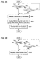
FIG. 5A and 5B are flow charts showing algorithms
in CPUs of a transmitter and a receiver according to the
present invention.
DETAILED DESCRIPTION OF THE PREFERRED EMBODIMENT
An embodiment of the present invention will be
described below in detail with reference to the
accompanying drawings.
Fig. 1 is a block diagram showing an example of a
transmitter according to the present invention. A
Transmitter 10 includes an SDH signal receiving circuit
11, a clock recovery circuit 12, a driving circuit 13,
a bias-T circuit 14, a bias adjusting circuit 15, an
Electrical-to-Optical (E/O) converter 16, and a CPU 17.
The SDH signal receiving circuit 11 receives an input
optical signal, the wavelength of which is in 1.3 µm band,
from an SDH device to convert the input optical signal
into a corresponding electrical signal. The clock recovery
circuit 12 recovers a clock signal from the electric signal
converted by the SDH signal receiving circuit 11. The
driving circuit 13 drives, for example, an external
modulator of the E/O converter 16. The bias-T circuit
14 and the bias adjusting circuit 15 give a bias voltage
to the modulator. The E/O converter 16 includes the
external modulator and a laser diode, which are not shown
in the Fig. 1.
The input optical signal from the SDH device is
received by the SDH signal receiving circuit 11 and
converted into an electric signal. The SDH receiving
circuit 11 monitors the power level of the input optical
signal. When the power level of the input signal is lower
than a predetermined level, the SDH receiving circuit
sends a "loss of signal" (LOS) alarm to the CPU 17. The
clock recovery circuit 12 recovers a clock signal from
the electric signal converted by the SDH receiving circuit
11 and detects a frame synchronous signal. When the clock
can not be recovered or when the frame synchronous can
not be established, the clock recovery circuit 12 sends
a "loss of lock" (LOL) alarm to the CPU 17.
When an optical fiber between the SDH device and
the SDH signal receiving circuit 11 is broken down or
an optical connector installed in the input port is
disconnected, the SDH signal receiving circuit 11 receives
no optical signal and sends the LOS alarm to the CPU 17.
When the transmitter receives the optical signal with
incorrect transmission rate, the clock recovery circuit
12 detects the out of synchronous signal and sends the
LOL alarm to the CPU 17.
The output of the clock recover circuit 12 is input
to the driving circuit 13 and is amplified to a swing
voltage enough to drive the external modulator in the
E/O converter 16. An input threshold value of the driving
circuit 13 is determined by a threshold signal output
from the CPU 17. The driving signal for the external
modulator is superimposed on a bias voltage set by the
bias adjusting circuit 15 through the bias-T circuit 14.
The bias voltage controlled by the CPU 17 is determined
by the extinction rate of the external modulator.
In the E/O converter 16, a light from a laser diode,
the wavelength of which is in 1.55 µm band, is modulated
in the external modulator by the driving signal
superimposed with a bias voltage, and is multiplexed by
an optical multiplexing filter together with other
wavelength multiplexing signal light.
Fig. 2 is a block diagram showing an example of the
receiver of the present invention. The receiver 20
includes an Optical-to-Electrical (O/E) converter 21,
a clock recovery circuit 22, an SDH signal generating
circuit 23, and a CPU 24. The O/E converter 21 receives
one of the WDM signal, the wavelength of which is in 1.55
µ m band and is de-multiplexed in an optical
de-multiplexing filter through an optical connector. The
O/E converter converts to the optical signal to the
corresponding electrical signal. The clock recovery
circuit 22 recovers a clock signal. The SDH signal
generating circuit 23 converts the electrical signal to
the corresponding optical signal with wavelength in 1.3
µm and sends the converted light to the SDH device.
The O/E converter 21 monitors the power level of
the input optical signal. When the power level of the
input signal is lower than a predetermined level, the
E/O converter sends "loss of signal" (LOS) alarm to the
CPU 24. The clock recovery circuit 22 recovers a clock
signal from the electric signal converted by the O/E
converter 21 and detects a frame synchronous signal. When
the clock can not be recovered or when the frame synchronous
can not be established, the clock recovery circuit 22
sends a "loss of lock" (LOL) alarm to the CPU 24.
When an optical transmission line between the
transmitter and the O/E converter is broken, or when an
optical connector installed in the input port of the
receiver is disconnected, the LOS alarm is sent to the
CPU 24 from the O/E converter 21. When a signal having
an incorrect rate is input to the O/E converter, the LOL
alarm is sent to the CPU 24. Receiving the LOS alarm or
the LOL alarm by the CPU 24, the CPU 24 sends the laser
diode shutting down signal to the SDH signal generating
circuit 23 to extinct the optical output. The optical
signal from the SDH signal generating circuit 23 is
transmitted to the SDH device through an optical connector
and an optical fiber.
Fig. 3 is a diagram showing an example of a WDM system
connecting two SDH devices. A transmitting station 301
is constituted by an SDH device 311, transmitters (10l
∼ 10N), an optical multiplexing filter 312, and an optical
amplifier 313. The transmitters (10l ∼ 10N) of N wavelengths
convert the input optical signals in 1.3 µm wavelength
band from the SDH device into the respective optical output
signal with 1.55 µm wavelength band for the WDM
transmission. The optical multiplexing filter 312
multiplexes the optical signals of the N wavelengths
output from the transmitters (10l ∼ 10N). The optical
amplifier 313 amplifies the WDM signal and transmits it
to an optical transmission line 303a.
A receiving station 302 is constituted by an optical
amplifier 321, an optical de-multiplexing filter 322,
receivers (20l ∼ 20N), and an SDH device 323. The optical
amplifier 321 receives the WDM signal from a transmission
line 303b. The optical de-multiplexing filter 322 divides
the multiplexed signal into serious of independent optical
signals with different wavelengths in 1.55 µm wavelength
band. The receivers (20l ∼ 20N) convert the input optical
signal to the corresponding optical signal of 1.3 µm
wavelength and sends the converted signal to the SDH
device.
A case will be described below when an input optical
signal of any one of the transmitters (10l ∼ 10N) is missed.
This case corresponds to the one that the optical fiber
between the SDH device and the SDH signal receiving circuit
is broken or the optical connector installed at the input
port is disconnected in Fig. 1. In such case, the SDH
signal receiving circuit 11 sends a LOS alarm to the CPU
17. The CPU 17 sends a threshold setting signal to the
driving circuit 13 to set the threshold voltage to the
predetermined value so as to fix the output of the driving
circuit to the high or low level, in which no output signal
generated from the driving circuit. Also, the CPU 17 sends
the bias setting signal to the bias adjusting circuit
15 to change the bias voltage superimposed on the out
put of the driving circuit 13.
By a serious control from the CUP 17, the output
of the E/O converter shows no modulation characteristics
and the power level of the output keeps substantially
equal to that in the modulated state. Since the power
level of the WDM signal transmitted in the transmission
line (303a and 303b) is maintained, optical signals not
missed in the transmitter normally transmitted to the
receiving station is not influenced by the signal
disappearing.
The receiver corresponds to the transmitter, the
optical signal of which is missed, receives an optical
signal with the equal level in the normal operation. In
this case, while the O/E circuit does not send the LOS
alarm, the clock recover circuit 22 sends the LOL alarm
to the CPU 24 because the input optical signal of the
receiver does not contain any clock signal nor frame
synchronous signal. The CPU 24 sends the laser diode
shutting down signal to the SDH signal generation circuit
23 to extinct the output of the receiver. By the operation
explained above, fault information generated in the SDH
device 311 can be transmitted through the WDM system to
the other SDH device 323 located downstream side of the
network.
Next explains a case in which an input signal of
any one of transmitters (10l ∼ 10N) becomes an incorrect
transmission rate. The SDH-signal receiving circuit 11
of the transmitter under concerned does not send a LOS
alarm because the receiving circuit 11 receives some
signal with incorrect rate. On the other hand, the clock
recovery circuit 12 sends the LOL alarm to the CPU because
the recovery circuit can not detect the frame synchronous
and set into the out-of-synchronous condition. The CPU
receiving the LOL alarm sends the threshold setting signal
to the driving circuit 13 to set the input threshold voltage
to the predetermined value so as to fix the output of
the driving circuit to the high or low level, in which
no signal is output from the circuit 13. Further to the
threshold setting signal, the CPU 17 sends the bias setting
signal to the bias adjusting circuit 15. By the serious
of controls explained above, the output of the E/O
converter 16 shows a non-modulated behavior arid its level
is equal to that of the normal state. Even if some
transmitter receives an optical signal with incorrect
rate, the output power level of the transmitter under
consideration keeps constant and the level of the light
transmitted in the WDM transmission line (303a, 303b)
is also maintained to be constant.
The optical signal with a power level equal to the
normal state is input to the receiver (any one of receivers
20l ∼ 20N) opposing to the transmitter to which the optical
signal with an incorrect rate is input. The O/E converter
21 of the receiver under concerned sends no LOS alarm
because some optical signal is input to the receiver 20.
While, the clock recovery circuit 22 sends the LOL alarm
to the CPU 24 because the recovery circuit can not detect
the clock or the frame synchronous signal from the
no-modulated electrical signal converted in the O/E
converter. The CPU 24 receiving the LOL alarm sends the
laser diode shutting signal to the SDH signal generating
circuit to extinct the optical output of the receiver.
Thus, fault information generated in the SDH device 311
in the transmitting station 301 can be transmitted to
the SDH device 323 of the receiving station 302.
Fig. 4 explains one switching algorithm of the bias
setting signal. Fig. 4 corresponds to the algorithm for
an external modulator of the electro-absorption type.
The CPU 17 receiving one of the LOS alarm or the LOL alarm
in the transmitter (10l ∼ 10N) sends the bias setting signal
to the bias adjusting circuit 15 to change the bias voltage
superimposed on the output signal of the driving circuit
13. The practical value of the bias voltage is determined
by the extinction ration of the external modulator. As
shown in Fig. 4, a bias voltage Vn, by which the normal
modulated signal is transmitted, and a voltage Vi
different from Vn, by which the un-modulated signal is
transmitted, are stored in the CPU 17. The CPU changes
the bias setting signal from Vn to Vi or Vi to Vn depending
on the conditions of the optical input.
Fig. 5A is a flow chart showing a control algorithm
of the CPU 17 in the transmitter. Fig. 5B is a flow chart
showing an algorithm of the CPU 24 in the receiver. In
Fig. 5A, the CPU 17 monitors an LOS alarm from the SDH
signal receiving circuit 11 or an LOL alarm from the clock
recovery circuit 12 (S501, S502). When the CPU detects
one of the alarms, the CPU sends a threshold setting signal
to the driving circuit 13 so as to fix the output of the
driving circuit 13 to "High" or "Low" level (S503).
Simultaneously, the CPU 17 sends the bias setting signal,
which is calculated from the relationship preliminary
stored in the CPU 17, to the bias adjusting circuit 15
(S505).
In Fig. 5B, the CPU 24 in the receiver 20 watches
an LOS alarm from the O/E converter 21 or an LOL alarm
from the clock recovery circuit 22 (S521, S522). When
either of alarms is detected, the CPU sends the laser
diode shutting down signal to the SDH signal generating
circuit 23 (S523) to vanish the optical output of the
receiver.
As described above, when some fault like the optical
input missing or the incorrect transmission ratio occur
in the transmitter, the optical output of this transmitter
for the WDM is set to be non-modulated and equivalent
level to the modulated state so that the LOL alarm can
be generated in the receiver without fail. Since it is
kept constant that the optical output of the transmitter
for the WDM and the input level of the optical amplifier
inserted into the transmission line, the deterioration
of the SNR or the over power of the receiver input can
be prevented. Moreover, since the fault information is
transmitted by the same wavelength with the signal
wavelength, spare transmitter and receiver are not
necessary and the transmission time difference between
the data and the fault information can be eliminated.
According to the present invention, when the
transmitter detects the optical input signal missing or
the incorrect transmission optical signal, the
transmitter outputs the optical signal with a
non-modulated and equal level to the modulated state.
When the receiver detects the non-modulated signal, the
receiver shuts down the optical output. By the method
above, even if one optical signal with certain wavelength
is missed or out of synchronous in the WDM transmission
system, optical signals with other wavelength can be
normally transmitted.