EP1172692A2 - Phase shift mask blank, phase shift mask, and methods of manufacture - Google Patents
Phase shift mask blank, phase shift mask, and methods of manufacture Download PDFInfo
- Publication number
- EP1172692A2 EP1172692A2 EP01305979A EP01305979A EP1172692A2 EP 1172692 A2 EP1172692 A2 EP 1172692A2 EP 01305979 A EP01305979 A EP 01305979A EP 01305979 A EP01305979 A EP 01305979A EP 1172692 A2 EP1172692 A2 EP 1172692A2
- Authority
- EP
- European Patent Office
- Prior art keywords
- phase shift
- shift mask
- substrate
- film
- mask blank
- Prior art date
- Legal status (The legal status is an assumption and is not a legal conclusion. Google has not performed a legal analysis and makes no representation as to the accuracy of the status listed.)
- Granted
Links
Images

Classifications
-
- G—PHYSICS
- G03—PHOTOGRAPHY; CINEMATOGRAPHY; ANALOGOUS TECHNIQUES USING WAVES OTHER THAN OPTICAL WAVES; ELECTROGRAPHY; HOLOGRAPHY
- G03F—PHOTOMECHANICAL PRODUCTION OF TEXTURED OR PATTERNED SURFACES, e.g. FOR PRINTING, FOR PROCESSING OF SEMICONDUCTOR DEVICES; MATERIALS THEREFOR; ORIGINALS THEREFOR; APPARATUS SPECIALLY ADAPTED THEREFOR
- G03F1/00—Originals for photomechanical production of textured or patterned surfaces, e.g., masks, photo-masks, reticles; Mask blanks or pellicles therefor; Containers specially adapted therefor; Preparation thereof
- G03F1/26—Phase shift masks [PSM]; PSM blanks; Preparation thereof
- G03F1/32—Attenuating PSM [att-PSM], e.g. halftone PSM or PSM having semi-transparent phase shift portion; Preparation thereof
-
- H—ELECTRICITY
- H10—SEMICONDUCTOR DEVICES; ELECTRIC SOLID-STATE DEVICES NOT OTHERWISE PROVIDED FOR
- H10P—GENERIC PROCESSES OR APPARATUS FOR THE MANUFACTURE OR TREATMENT OF DEVICES COVERED BY CLASS H10
- H10P76/00—Manufacture or treatment of masks on semiconductor bodies, e.g. by lithography or photolithography
Definitions
- the present invention relates to phase shift mask blanks and phase shift masks for use in the microfabrication of high-density semiconductor integrated circuits such as large-scale integration (LSI) and very large-scale integration (VLSI) chips, charge-coupled devices, color filters for liquid-crystal displays, and magnetic heads.
- the invention relates also to methods of manufacturing such phase shift mask blanks and phase shift masks. More particularly, the invention relates to halftone phase shift mask blanks and phase shift masks which can attenuate the intensity of exposure wavelength light with a phase shift film, and to methods of manufacturing such phase shift mask blanks and phase shift masks.
- the photomasks that are used in a broad range of applications including the manufacture of semiconductor integrated circuits (IC) and LSI chips, are basically composed of a transparent substrate on which a light-shielding layer made primarily of chromium has been formed in a given pattern.
- IC semiconductor integrated circuits
- LSI chips are basically composed of a transparent substrate on which a light-shielding layer made primarily of chromium has been formed in a given pattern.
- the market demand for ever higher levels of integration in semiconductor integrated circuits has led to a rapid reduction in the minimum feature size of photomask patterns. Such miniaturization has been achieved in part by the use of exposure light of shorter wavelengths.
- phase shifting One pattern transfer technique that has been effective for resolving such problems is phase shifting. This involves the use of a phase shift mask as the mask for transferring patterns having a small minimum feature size.
- a phase shift mask typically has a phase shifter 2a that forms a patterned area on the mask and an area 1a without phase shifter where the substrate lies exposed to incident light.
- the phase shift mask improves contrast of the transferred image by providing a phase difference of 180 degrees between light passing through the patterned and unpatterned areas, and utilizing the destructive interference of light at the boundary regions of the pattern to set the light intensity in the interference regions to zero.
- the use of phase shifting also makes it possible to increase the focal depth at the necessary resolution.
- the use of a phase shift mask can improve resolution and increase the margin of the exposure process.
- phase shift masks can be broadly categorized, according to the light-transmitting characteristics of the phase shifter, as either completely transmitting phase shift masks or halftone phase shift masks.
- Completely transmitting phase shift masks are masks in which the phase shifter has the same light transmittance as the substrate, and which are thus transparent to light at the exposure wavelength.
- the phase shifter has a light transmittance that ranges from about several percent to several tens of percent the transmittance of exposed substrate areas (unpatterned areas).
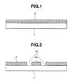
- FIG. 1 shows the basic structure of a halftone phase shift mask blank
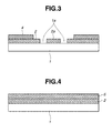
- FIG. 2 shows the basic structure of a halftone phase shift mask.
- the halftone phase shift mask blank shown in FIG. 1 is composed of a substrate 1 which is transparent to the exposure light, and on which a halftone phase shift film 2 has been formed.
- the halftone phase shift mask shown in FIG. 2 is composed of a halftone phase shifter 2a which forms the patterned areas of the mask, and exposed substrate areas 1a on which there is no phase shift film.
- Exposure light that has passed through the phase shifter 2a is phase-shifted relative to exposure light that has passed through exposed substrate areas 1a.
- the transmittance of the phase shifter 2a is selected such that exposure light which has passed through the phase shifter 2a has too low an intensity to sensitize the resist on the substrate to which the pattern is being transferred. Accordingly, the phase shifter functions to substantially shield out exposure light.
- the above-described halftone phase shift mask include halftone phase shift masks having a simple, single-layer structure.
- Single-layer halftone phase shift masks known to the art include those described in JP-A 7-140635 which have a phase shifter composed of molybdenum silicide oxide (MoSiO) or molybdenum silicide oxide nitride (MoSiON).
- MoSiO molybdenum silicide oxide
- MoSiON molybdenum silicide oxide nitride
- a lithographic process may be used to manufacture such phase shift masks.
- the lithographic process typically involves applying a resist onto the phase shift mask blank, sensitizing desired areas of the resist with electron beams or ultraviolet light, carrying out development to expose the surface of the phase shift film, then etching the desired areas of the phase shift film using the patterned resist film as the mask so as to expose the substrate.
- the resist film is then stripped, giving the finished phase shift mask.
- the etching process employed for this purpose is generally reactive ion etching with a fluorine-containing gas.
- the material ordinarily used as the transparent substrate is quartz.
- phase shift mask substrate By the time etching is complete over all areas where the substrate is to be exposed, the amount of phase shift ends up differing between those areas within the substrate plane where the substrate surface becomes exposed a little earlier and those areas where it becomes exposed a little later. As a result, the distribution in phase shift within the plane of the phase shift mask substrate worsens, making it difficult to stably manufacture high-quality phase shift masks having a high in-plane uniformity in the phase shift.
- the general aim herein is to provide new and useful phase shift mask blanks and phase shift masks (and in other aspects, methods in which these are made and used) having good uniformity of the phase shift over the exposed areas.
- phase shift film having a large etch selectivity relative to the substrate i.e. etch rate ratio under actual or typical conditions used in manufacture
- phase shift films of molybdenum silicide oxide carbide (MoSiOC) and/or molybdenum silicide oxide nitride carbide (MoSiONC) are excellent from the point of view of improving phase shift uniformity, and can give good etch selectivity as between film and substrate e.g. to the ratio mentioned above.
- the invention provides a phase shift mask blank having a transparent substrate and at least one phase shift film layer composed primarily of a metal and silicon on the substrate, wherein the substrate has an etch rate A and the phase shift film has an etch rate B when the blank is patterned by reactive ion etching such that the etch selectivity B/A is at least 5.0.
- the phase shift film is preferably made of molybdenum silicide oxide carbide or molybdenum silicide oxide nitride carbide. Typically, it changes the phase of exposure light passing through it by 180 ⁇ 5 degrees. Preferably it has a transmittance of from 3 to 40%.
- the invention provides a phase shift mask (or blank therefor) in which at least one phase shift film on a transparent substrate, preferably at least a said film adjacent the substrate, is of MoSiOC or MoSiONC.
- the invention provides a phase shift mask manufactured by lithographically patterning the phase shift mask blank of the first aspect of the invention.
- the invention provides a method of manufacturing a phase shift mask blank having a transparent substrate and at least one phase shift film layer composed primarily of a metal and silicon on the substrate, in which method reactive sputtering is carried out using a molybdenum and silicon-containing target and a carbon-containing gas.
- the substrate prefferably has an etch rate A and the phase shift film to have an etch rate B when the blank is patterned by reactive ion etching such that the etch selectivity B/A is at least 5.0.
- Reactive sputtering is typically carried out using carbon dioxide as the carbon-containing gas.
- the phase shift film preferably changes the phase of exposure light passing through it by 180 ⁇ 5 degrees and has a transmittance of 3 to 40%.
- the invention provides a method of manufacturing a phase shift mask by lithographically patterning the phase shift mask blank made by the method according to the fourth aspect of the invention.
- the invention increases the phase shift film etch rate in a halftone phase shift mask blank so as to make the difference between this rate and the substrate etch rate larger.
- deviations from the desired phase shift due to overetching of the substrate can be reduced, making it possible to manufacture, with good control and stability, high-quality phase shift masks having a uniform phase shift distribution within the plane of the substrate.
- phase shift masks can be used to fabricate semiconductor integrated circuits to a smaller minimum feature size and higher level of integration.
- FIG. 1 is a sectional view of a phase shift mask blank according to one embodiment of the invention.
- FIG. 2 is a sectional view of a phase shift mask made from the same blank.
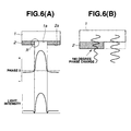
- FIG. 3 is a sectional view of a phase shift mask according to another embodiment of the invention.
- FIG. 4 is a sectional view of the phase shift mask blank from which the phase shift mask in FIG. 3 is made.
- FIG. 5 are schematic sectional views illustrating the method of manufacturing phase shift masks according to the invention.
- FIG. 5A shows the mask blank on which a resist film has been formed
- FIG. 5B shows the mask workpiece after the resist film has been patterned
- FIG. 5C shows the workpiece after etching has been carried out
- FIG. 5D shows the completed mask after the resist film has been removed.
- FIGS. 6A and 6B illustrate the operating principle of a halftone phase shift mask.
- FIG. 6B is an enlarged view of region X in FIG. 6A.
- the phase shift mask blank of the invention is made up of a substrate 1 which is transparent to the exposure light and a phase shift film 2 composed primarily of a metal and silicon that has been formed on the substrate 1.
- the substrate has an etch rate A and the phase shift film has an etch rate B when the phase shift mask blank is patterned by reactive ion etching such that the etch selectivity B/A is at least 5.0.
- An etch selectivity of at least 5.0 can be achieved by regulating the composition of the phase shift film. This involves adjusting the relative proportion of components which slow the etch rate in the phase shift layer and components which speed up the etch rate.
- the phase shift film is composed primarily of a metal and silicon.
- the film is preferably made of molybdenum silicide oxide carbide (MoSiOC) or molybdenum silicide oxide nitride carbide (MoSiONC).
- MoSiOC molybdenum silicide oxide carbide
- MoSiONC molybdenum silicide oxide nitride carbide
- phase shift film it is advantageous for the phase shift film to change the phase of exposure light passing through it by 180 ⁇ 5 degrees. 'Transmittance for that light is preferably 3 to 40%.
- the transparent substrate used together with the phase shift film is composed primarily of quartz or silicon dioxide.
- the phase shift film is not necessarily limited to a single layer.
- the phase shift mask of the invention may include a light-shielding film 4 that has been formed over the phase shift film 2.
- a chromium-based film such as CrO, CrN, CrON, or CrCON as the light-shielding film is preferred.
- phase shift film 2 having the desirable selectivity (e.g. ⁇ 5) and to form on the first layer 2 a second phase shift film 5 which may have ordinary selectivity with respect to the substrate 1 e.g. less than 5.0, so as to give a phase shift film having a multilayer structure in which the etch rate increases in a continuous or stepwise manner from the surface side to the transparent substrate side.
- a film structure can be adopted in which the etch rate of the phase shift film is varied in a continuous or stepwise manner so that the etch selectivity on the substrate side becomes at least 5.0.
- the phase shift film in the invention is preferably formed by reactive sputtering in which the sputtering target is composed primarily of a metal and silicon.
- the target may be composed entirely of a metal and silicon, although a target in which one or more elements selected from among oxygen, nitrogen and carbon has been added to the metal may be used to keep the film composition constant within the plane of the film. Molybdenum is preferred as the metal.
- the sputtering process may be one which employs a direct-current power supply (DC sputtering) or a highfrequency power supply (RF sputtering). Either a magnetron sputtering system or a conventional sputtering system may be used.
- the film-forming system may be either a continuous, in-line system or a single-workpiece processing system.
- the sputtering gas used during formation of the phase shift film may be composed of an inert gas such as argon to which have been suitably added oxygen, nitrogen, a nitrogen oxide gas, and a carbon-containing gas such as a carbon oxide gas.
- exemplary carbon-containing gases include hydrocarbon gases such as methane, and the carbon oxide gases carbon monoxide and carbon dioxide.
- the use of carbon dioxide is especially preferred because, in addition to serving as both a carbon source and an oxygen source, it is a stable gas having a low reactivity.
- the sputtering gas used to form a MoSiOC or MoSiONC film is composed of an inert gas such as argon and a carbon-containing mixed gas as the carbon source.
- gases such as oxygen, nitrogen and nitrogen oxide gases may be suitably added so as to give the phase shift film that is formed the desired composition.
- formation of a MoSiOC film is preferably carried out by reactive sputtering using molybdenum silicide as the sputtering target and a combination of argon and carbon dioxide as the sputtering gas.
- Formation of a MoSiONC film is preferably carried out by reactive sputtering using molybdenum silicide as the target and a combination of argon, carbon dioxide and nitrogen as the sputtering gas.
- the transmittance of the phase shift film which forms may be raised by increasing the amount of oxygen and nitrogen-containing gases added to the sputtering gas or by using as the sputtering target a metal silicide to which a large amount of oxygen and nitrogen have been added, so that more oxygen and nitrogen are incorporated into the film.
- a phase shift mask as shown in FIG.2 is typically made from the phase shift mask blank by first forming the phase shift film 12 on a transparent substrate 11 and then forming a resist film 13 on the phase shift film 12 (FIG. 5A). Next, the resist film 13 is patterned (FIG. 5B), after which the phase shift film 12 is etched (FIG. 5C). The resist film 13 is subsequently stripped (FIG. 5D). In this process, application of the resist film, patterning (exposure and development), and resist film removal may be carried out by known techniques.
- Etching is preferably carried out by a dry etching process, and most preferably reactive ion etching (RIE). Reactive ion etching may be performed using a reactive ion etching system.
- the etching gas is preferably a fluorine-containing gas such as CF 4 , either used by itself or in combination with any of argon, helium and oxygen.
- the resulting phase shift mask can be formed with minimal deviation from the desired phase shift due to overetching of the substrate, and thus has a uniform phase shift distribution within the plane of the substrate, making it well-suited to the fabrication of semiconductor integrated circuits to a smaller minimum feature size and a higher level of integration.
- a MoSiONC film was formed on a quartz substrate to a thickness of 140 nm by carrying out reactive sputtering in a sputtering system using molybdenum silicide as the target and using a mixture of argon, carbon dioxide and nitrogen in a flow rate ratio of 5:3:3 as the sputtering gas.
- phase shift film was found to provide a phase shift of 182 degrees and a transmittance of 8.3%.
- the composition of the phase shift film as determined by x-ray photoelectron spectroscopy (XPS), was 14 atom % molybdenum, 23 atom % silicon, 46 atom % oxygen, 10 atom % nitrogen, and 8 atom % carbon.
- a MoSiON film was formed to a thickness of 130 nm in the same way as in Example 1, giving a phase shift film which provided a phase shift for 248 nm light of 182 degrees and a transmittance of 7.0%.
- the composition of the phase shift film as determined by XPS, was 13 atom % molybdenum, 26 atom % silicon, 47 atom % oxygen, and 14 atom % nitrogen. The level of carbon was below the limit of detection.
- phase shift mask blank was reactive ion etched under the same conditions as in Example 1, resulting in a phase shift film etch rate of 28.7 nm/min.
- the quartz substrate etch rate under the same conditions was 6.2 nm/min. Hence, the etch selectivity was 4.6.
- Table 1 Etched material Etch rate (nm/min) Etch selectivity versus substrate quartz substrate 6.2
- Example 1 From the results in Table 1, it is apparent that the MoSiONC film in Example 1 had a higher etch rate than the MoSiON film in Comparative Example 1. Hence, in Example 1, overetching of the substrate in the reaction ion etching step during phase shift mask production results in little deviation from the selected phase shift value, making it possible to improve the in-plane uniformity of the phase shift.
- the present invention by using a phase shift film which has a larger etch selectivity with respect to the substrate and is preferably made of MoSiOC or MoSiONC, provides high-quality phase shift mask blanks and phase shift masks which have little deviation from the selected phase shift values due to overetching in the reactive ion etching step of mask fabrication, and thus have an improved in-plane uniformity in the phase shift.
Landscapes
- Physics & Mathematics (AREA)
- General Physics & Mathematics (AREA)
- Preparing Plates And Mask In Photomechanical Process (AREA)
- Drying Of Semiconductors (AREA)
Abstract
Description
| Etched material | Etch rate (nm/min) | Etch selectivity versus substrate | |
| quartz substrate | 6.2 | ||
| Example 1 | MoSiONC | 35.0 | 5.6 |
| Comparative Example 1 | MoSiON | 28.7 | 4.6 |
Claims (9)
- A phase shift mask blank comprising a transparent substrate and at least one phase shift film layer composed primarily of a metal and silicon on the substrate, wherein the substrate has an etch rate A and the phase shift film has an etch rate B when the blank is patterned by reactive ion etching such that the etch selectivity B/A is at least 5.0.
- The phase shift mask blank of claim 1, wherein the phase shift film is made of molybdenum silicide oxide carbide or molybdenum silicide oxide nitride carbide.
- The phase shift mask blank of claim 1, wherein the phase shift film changes the phase of exposure light passing through it by 180±5 degrees and has a transmittance of 3 to 40%.
- A phase shift mask manufactured by lithographically patterning the phase shift mask blank of claim 1.
- A method of manufacturing a phase shift mask blank having a transparent substrate and at least one phase shift film layer composed primarily of a metal and silicon on the substrate, the method comprising the step of carrying out reactive sputtering using a molybdenum and silicon-containing target and using a carbon-containing sputtering gas.
- The phase shift mask blank manufacturing method of claim 5, wherein the substrate has an etch rate A and the phase shift film has an etch rate B when the blank is patterned by reactive ion etching such that the etch selectivity B/A is at least 5.0.
- The phase shift mask blank manufacturing method of claim 5, wherein reactive sputtering is carried out using carbon dioxide as the carbon-containing gas.
- The phase shift mask blank manufacturing method of claim 5, wherein the phase shift film changes the phase of exposure light passing through it by 180±5 degrees and has a transmittance of 3 to 40%.
- A method of manufacturing a phase shift mask by lithographically patterning the phase shift mask blank made by the method of claim 5.
Applications Claiming Priority (2)
| Application Number | Priority Date | Filing Date | Title |
|---|---|---|---|
| JP2000212782A JP2002023342A (en) | 2000-07-13 | 2000-07-13 | Phase shift mask blank, phase shift mask, and manufacturing method thereof |
| JP2000212782 | 2000-07-13 |
Publications (3)
| Publication Number | Publication Date |
|---|---|
| EP1172692A2 true EP1172692A2 (en) | 2002-01-16 |
| EP1172692A3 EP1172692A3 (en) | 2002-07-24 |
| EP1172692B1 EP1172692B1 (en) | 2004-09-29 |
Family
ID=18708650
Family Applications (1)
| Application Number | Title | Priority Date | Filing Date |
|---|---|---|---|
| EP01305979A Expired - Lifetime EP1172692B1 (en) | 2000-07-13 | 2001-07-11 | Phase shift mask blank, phase shift mask, and methods of manufacture |
Country Status (6)
| Country | Link |
|---|---|
| US (1) | US6641958B2 (en) |
| EP (1) | EP1172692B1 (en) |
| JP (1) | JP2002023342A (en) |
| KR (1) | KR100552876B1 (en) |
| DE (1) | DE60105904T2 (en) |
| TW (1) | TW520462B (en) |
Families Citing this family (10)
| Publication number | Priority date | Publication date | Assignee | Title |
|---|---|---|---|---|
| KR100669862B1 (en) * | 2000-11-13 | 2007-01-17 | 삼성전자주식회사 | Method of forming fine pattern of semiconductor device |
| JP4600629B2 (en) * | 2001-06-26 | 2010-12-15 | 信越化学工業株式会社 | Phase shift mask blank and manufacturing method thereof |
| US7011910B2 (en) * | 2002-04-26 | 2006-03-14 | Hoya Corporation | Halftone-type phase-shift mask blank, and halftone-type phase-shift mask |
| TWI305865B (en) | 2003-03-31 | 2009-02-01 | Shinetsu Chemical Co | Photomask blank, photomask, and method of manufacture |
| WO2004088421A1 (en) | 2003-03-31 | 2004-10-14 | Hoya Corporation | Mask blank, mask blank manufacturing method, transfer mask manufacturing method, and semiconductor device manufacturing method |
| JP2004302024A (en) * | 2003-03-31 | 2004-10-28 | Shin Etsu Chem Co Ltd | Phase shift mask blank, phase shift mask, and method of forming phase shift film |
| KR100546365B1 (en) * | 2003-08-18 | 2006-01-26 | 삼성전자주식회사 | Blank photomask and manufacturing method of the photomask using the same |
| JP5105407B2 (en) * | 2007-03-30 | 2012-12-26 | Hoya株式会社 | Photomask blank, photomask and photomask manufacturing method |
| KR101152618B1 (en) * | 2010-02-12 | 2012-06-05 | 주식회사 에스앤에스텍 | Half-tone phase shift blankmask, half-tone phase shift photomask and manutacturing methods of the same |
| KR101197250B1 (en) * | 2010-04-23 | 2012-11-05 | 주식회사 에스앤에스텍 | Blankmask, Photomask and manutacturing method of the same |
Family Cites Families (6)
| Publication number | Priority date | Publication date | Assignee | Title |
|---|---|---|---|---|
| JP3064769B2 (en) | 1992-11-21 | 2000-07-12 | アルバック成膜株式会社 | PHASE SHIFT MASK, ITS MANUFACTURING METHOD, AND EXPOSURE METHOD USING THE PHASE SHIFT MASK |
| JP3397933B2 (en) * | 1995-03-24 | 2003-04-21 | アルバック成膜株式会社 | Phase shift photomask blanks, phase shift photomasks, and manufacturing methods thereof. |
| US5635315A (en) * | 1995-06-21 | 1997-06-03 | Hoya Corporation | Phase shift mask and phase shift mask blank |
| US5942356A (en) * | 1996-03-30 | 1999-08-24 | Hoya Corporation | Phase shift mask and phase shift mask blank |
| US6309780B1 (en) * | 1998-03-09 | 2001-10-30 | Rochester Institute Of Technology | Attenuated phase shift mask and a method for making the mask |
| EP1117000B1 (en) * | 2000-01-12 | 2004-01-02 | Shin-Etsu Chemical Co., Ltd. | Phase shift mask blank, phase shift mask, and method of manufacture |
-
2000
- 2000-07-13 JP JP2000212782A patent/JP2002023342A/en active Pending
-
2001
- 2001-07-11 EP EP01305979A patent/EP1172692B1/en not_active Expired - Lifetime
- 2001-07-11 DE DE60105904T patent/DE60105904T2/en not_active Expired - Lifetime
- 2001-07-12 KR KR1020010041873A patent/KR100552876B1/en not_active Ceased
- 2001-07-12 TW TW090117115A patent/TW520462B/en not_active IP Right Cessation
- 2001-07-12 US US09/902,645 patent/US6641958B2/en not_active Expired - Lifetime
Also Published As
| Publication number | Publication date |
|---|---|
| EP1172692A3 (en) | 2002-07-24 |
| DE60105904D1 (en) | 2004-11-04 |
| KR100552876B1 (en) | 2006-02-20 |
| US6641958B2 (en) | 2003-11-04 |
| KR20020007181A (en) | 2002-01-26 |
| DE60105904T2 (en) | 2005-11-03 |
| EP1172692B1 (en) | 2004-09-29 |
| US20020025478A1 (en) | 2002-02-28 |
| TW520462B (en) | 2003-02-11 |
| JP2002023342A (en) | 2002-01-23 |
Similar Documents
| Publication | Publication Date | Title |
|---|---|---|
| US7314690B2 (en) | Photomask producing method and photomask blank | |
| KR0151883B1 (en) | Phase shift mask and its manufacturing method | |
| KR100758052B1 (en) | Phase Shift Photo Mask and Phase Shift Photo Mask Dry Etching Method | |
| EP1182504B1 (en) | Phase shift mask blank, phase shift mask, and methods of manufacture | |
| KR20000057061A (en) | Photomask and manufacturing method thereof, and exposure method using the photomask | |
| KR20080059614A (en) | Photomask blanks, a method of manufacturing the same, a method of manufacturing a photomask, and a method of manufacturing a semiconductor device | |
| US6503668B2 (en) | Phase shift mask blank, phase shift mask, and method of manufacture | |
| US7037625B2 (en) | Phase shift mask blank and method of manufacture | |
| KR100520014B1 (en) | Phase shift mask and method of manufacturing phase shift mask | |
| JPH04233541A (en) | Photomask and method for correcting defect in the same | |
| EP1172692B1 (en) | Phase shift mask blank, phase shift mask, and methods of manufacture | |
| US20010006754A1 (en) | Phase shift mask blank, phase shift mask and method of manufacture | |
| EP1194813A1 (en) | Phase-shift photomask for patterning high density features | |
| JP3696320B2 (en) | Phase shift mask, phase shift mask blank, and manufacturing method thereof | |
| US7122453B2 (en) | Methods of patterning radiation, methods of forming radiation-patterning tools, and radiation-patterning tools | |
| JP3312702B2 (en) | Phase shift photomask and blank for phase shift photomask | |
| JP2004302078A (en) | Phase shift mask blank, phase shift mask, and manufacturing method thereof | |
| JP3645888B2 (en) | Halftone phase shift mask | |
| US20090053620A1 (en) | Blank Mask and Method for Fabricating Photomask Using the Same | |
| JP2002189284A (en) | Phase shift mask blank, phase shift mask, and method of manufacturing phase shift mask blank and phase shift mask | |
| JPH1184624A (en) | Blank for halftone type phase shift mask, halftone type phase shift mask, and manufacturing method thereof | |
| JP2003195474A (en) | Phase shift mask blank, phase shift mask, and manufacturing method thereof | |
| US6562521B1 (en) | Semiconductor feature having support islands | |
| JP2004317547A (en) | Blank for halftone type phase shift mask, method of manufacturing the same, and halftone type phase shift mask | |
| JPH04258955A (en) | Production of phase shift mask |
Legal Events
| Date | Code | Title | Description |
|---|---|---|---|
| PUAI | Public reference made under article 153(3) epc to a published international application that has entered the european phase |
Free format text: ORIGINAL CODE: 0009012 |
|
| AK | Designated contracting states |
Kind code of ref document: A2 Designated state(s): AT BE CH CY DE DK ES FI FR GB GR IE IT LI LU MC NL PT SE TR |
|
| AX | Request for extension of the european patent |
Free format text: AL;LT;LV;MK;RO;SI |
|
| PUAL | Search report despatched |
Free format text: ORIGINAL CODE: 0009013 |
|
| AK | Designated contracting states |
Kind code of ref document: A3 Designated state(s): AT BE CH CY DE DK ES FI FR GB GR IE IT LI LU MC NL PT SE TR |
|
| AX | Request for extension of the european patent |
Free format text: AL;LT;LV;MK;RO;SI |
|
| 17P | Request for examination filed |
Effective date: 20021024 |
|
| AKX | Designation fees paid |
Designated state(s): DE FR GB IT |
|
| 17Q | First examination report despatched |
Effective date: 20030319 |
|
| GRAP | Despatch of communication of intention to grant a patent |
Free format text: ORIGINAL CODE: EPIDOSNIGR1 |
|
| GRAS | Grant fee paid |
Free format text: ORIGINAL CODE: EPIDOSNIGR3 |
|
| GRAA | (expected) grant |
Free format text: ORIGINAL CODE: 0009210 |
|
| RIN1 | Information on inventor provided before grant (corrected) |
Inventor name: KANEKO, HIDEO,C/O ADVANCED FUNCTIONAL MATERIALS Inventor name: MARUYAMA, TAMOTSU,C/O ADVANCED FUNCTIONAL Inventor name: KOJIMA, MIKIO,C/O ADVANCED FUNCTIONAL MATERIALS Inventor name: OKAZAKI, SATOSHI,ADVANCED FUNCTIONAL MATERIALS Inventor name: WATANABE, MASATAKA,ADVANCED FUNCTIONAL MATERIALS Inventor name: INAZUKI, YUKIO,C/O ADVANCED FUNCTIONAL MATERIALS |
|
| AK | Designated contracting states |
Kind code of ref document: B1 Designated state(s): DE FR GB IT |
|
| REG | Reference to a national code |
Ref country code: GB Ref legal event code: FG4D |
|
| REG | Reference to a national code |
Ref country code: IE Ref legal event code: FG4D |
|
| REF | Corresponds to: |
Ref document number: 60105904 Country of ref document: DE Date of ref document: 20041104 Kind code of ref document: P |
|
| PLBE | No opposition filed within time limit |
Free format text: ORIGINAL CODE: 0009261 |
|
| STAA | Information on the status of an ep patent application or granted ep patent |
Free format text: STATUS: NO OPPOSITION FILED WITHIN TIME LIMIT |
|
| ET | Fr: translation filed | ||
| 26N | No opposition filed |
Effective date: 20050630 |
|
| REG | Reference to a national code |
Ref country code: FR Ref legal event code: PLFP Year of fee payment: 16 |
|
| REG | Reference to a national code |
Ref country code: FR Ref legal event code: PLFP Year of fee payment: 17 |
|
| REG | Reference to a national code |
Ref country code: FR Ref legal event code: PLFP Year of fee payment: 18 |
|
| PGFP | Annual fee paid to national office [announced via postgrant information from national office to epo] |
Ref country code: GB Payment date: 20180711 Year of fee payment: 18 |
|
| GBPC | Gb: european patent ceased through non-payment of renewal fee |
Effective date: 20190711 |
|
| PG25 | Lapsed in a contracting state [announced via postgrant information from national office to epo] |
Ref country code: GB Free format text: LAPSE BECAUSE OF NON-PAYMENT OF DUE FEES Effective date: 20190711 |
|
| PGFP | Annual fee paid to national office [announced via postgrant information from national office to epo] |
Ref country code: FR Payment date: 20200611 Year of fee payment: 20 |
|
| PGFP | Annual fee paid to national office [announced via postgrant information from national office to epo] |
Ref country code: DE Payment date: 20200630 Year of fee payment: 20 |
|
| PGFP | Annual fee paid to national office [announced via postgrant information from national office to epo] |
Ref country code: IT Payment date: 20200610 Year of fee payment: 20 |
|
| REG | Reference to a national code |
Ref country code: DE Ref legal event code: R071 Ref document number: 60105904 Country of ref document: DE |