EP1170886A2 - Control and communication system for components of electrical apparatus - Google Patents
Control and communication system for components of electrical apparatus Download PDFInfo
- Publication number
- EP1170886A2 EP1170886A2 EP01116063A EP01116063A EP1170886A2 EP 1170886 A2 EP1170886 A2 EP 1170886A2 EP 01116063 A EP01116063 A EP 01116063A EP 01116063 A EP01116063 A EP 01116063A EP 1170886 A2 EP1170886 A2 EP 1170886A2
- Authority
- EP
- European Patent Office
- Prior art keywords
- light
- electrical apparatus
- components
- data
- receiver
- Prior art date
- Legal status (The legal status is an assumption and is not a legal conclusion. Google has not performed a legal analysis and makes no representation as to the accuracy of the status listed.)
- Withdrawn
Links
Images
Classifications
-
- H—ELECTRICITY
- H05—ELECTRIC TECHNIQUES NOT OTHERWISE PROVIDED FOR
- H05K—PRINTED CIRCUITS; CASINGS OR CONSTRUCTIONAL DETAILS OF ELECTRIC APPARATUS; MANUFACTURE OF ASSEMBLAGES OF ELECTRICAL COMPONENTS
- H05K1/00—Printed circuits
- H05K1/02—Details
- H05K1/0274—Optical details, e.g. printed circuits comprising integral optical means
-
- H—ELECTRICITY
- H04—ELECTRIC COMMUNICATION TECHNIQUE
- H04B—TRANSMISSION
- H04B10/00—Transmission systems employing electromagnetic waves other than radio-waves, e.g. infrared, visible or ultraviolet light, or employing corpuscular radiation, e.g. quantum communication
- H04B10/80—Optical aspects relating to the use of optical transmission for specific applications, not provided for in groups H04B10/03 - H04B10/70, e.g. optical power feeding or optical transmission through water
- H04B10/801—Optical aspects relating to the use of optical transmission for specific applications, not provided for in groups H04B10/03 - H04B10/70, e.g. optical power feeding or optical transmission through water using optical interconnects, e.g. light coupled isolators, circuit board interconnections
Definitions
- This invention relates to a means for allowing communication between components within electrical apparatus and thus control of said components.
- the invention can be of use with any form of electrical apparatus, and one such form is a receiver for the reception of broadcast data and decoding/processing of the same.
- a broadcast data receiver it should be appreciated that the invention is not limited to this particular form of apparatus in any way.
- a further problem is that in addition to conducted electrical interference, in the PCB of the receiver interference is radiated due to track lengths and source load mismatch of the connecting tracks.
- PCBs that carry high speed data such as memory buses and MPEG bit streams account for more than 50% of all the tracks on a PCB.
- Digital pulses with rise and fall times of a few nano seconds produce radiated and conducted electrical signals of several hundred MHz, and this is the main source of Electro Magnetic Compatibility (EMC) and Radio Frequency Interference (RFI) problems encountered in receivers.
- EMC Electro Magnetic Compatibility
- RFID Radio Frequency Interference
- the aim of the present invention is to provide a means whereby at least two components of the PCB can be connected to allow the transmission of data between the two without or with reduced electrical interference.
- a further aim of the present invention is to allow communication between the components in a manner which ensures that the overall configuration of the apparatus can be in as cost effective a manner as possible.
- electrical apparatus said electrical apparatus including a number of components which are required to communicate with each other in a manner to allow the transmission of data therebetween, and characterised in that at least two of the components are provided with communication means to allow said communication of data in the form of a light emitter and receiver, and communication is made by the controlled emission of light and the reception of the same.
- the communication means comprise what are hereinafter referred to as a 'light aerial' for the transmission and reception of data.
- the communication means includes a series of LED's and Photo receptors which are provided to communicate with each other. This communication is achieved by allowing the light to radiate from the LED's and throughout a housing of the electrical apparatus in which the components are provided.
- light data signals can be transmitted from one component to the other via a conduit, such as a fibre optic cable connection.
- the electrical apparatus is a broadcast data receiver.
- infra red (IF) light emitters and transmitters are used.
- the two tuners are controlled by two independent I 2 C buses (i.e., with in line filters and eight PCB tracks).
- I 2 C buses i.e., with in line filters and eight PCB tracks.
- Two IR transceivers are required, one transceiver is required for the controller IC and one transceiver is required for the two tuners.
- the slow data rate of IR transceivers is suitable for such I 2 C bus systems.
- the addition of further IR transceivers or receive only devices for other components conventionally suffering from electrical interference, such as the TV re-modulator and the SCART switch functions, can also be employed.
- a BDR receiving digital data from a broadcaster at a remote location and decoding said data to provide video, audio and/or auxiliary data
- said BDR including one or more printed circuit boards and said one or boards including a number of components which are required to be interconnected in a manner to allow the transmission of data therebetween, characterised in that at least two of said components are provided with communication means to allow said communication of data and said communication means are in the form of a light emitter and receiver.
- the advantages of employing a light communication method are that conducted electrical interference normally associated with copper PCB tracks is not present.
- the light communication method allows single or double-sided PCBs to be used rather than multi layer PCBs and reduces the EMC/RFI fixing required, thereby reducing the cost of manufacturing the BDR or apparatus.
- the light communication method is employed as part of the silicon, i.e., a window is available in the IC package such that it is able to transmit/receive light directly on the silicon die, then again the cost of manufacturing the BDR/apparatus is significantly reduced.
- the light communication method does not require a line of sight transmission path as communication distances within broadcast data receivers, and also other electrical equipment, are generally small and there are many surfaces against which the light can be reflected. Signal attenuation is not a problem with the light method as again the communication distances are small.
- multi-path interference is not an issue as multi path interference is short in duration compared with the data transmission rate.
- a yet further advantage of the present invention is the provision of being able to electrically isolate two circuit paths.
- both high and low speed light connectivity can be employed within a BDR/apparatus using the light method, there is no longer the need to physically connect electrical interference generation circuits to electrical interference sensitive circuits.
- PCB printed circuit board
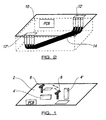
- the PCB 2 has a number of components 4 mounted thereon for illustrative purposes. In practice there will be many more components than is shown.
- each aerial is provided with at least one light source such as an LED which is controllable to emit light at required times.
- the emitted light is free to pass around the BDR housing (not shown) and deflect off the walls, sides, lid, PCB and associated components, and/or floor of the BDR housing, which when fitted encloses the components and forms the external surface of the BDR.
- each aerial or component is provided with light detecting and receiving means, such as a photo receptor.
- the photo receptor is set to receive and process light which is transmitted at a certain specified wavelength such that the correct data is received and can then be processed. This therefore allows the appropriate data to be processed and communication between the correct components to be achieved.
- a PCB 10 is provided with components 12', 12" mounted thereon. These two components are required to be interconnected to allow the transmission of data between the same. This embodiment is particularly suited to high data rate transmission where directional signal transmission is required to avoid multi-path problems.
- the light data signals are routed along fibre optic type conduits 14. If the light conduits are made into a " light mat" which is placed under but in contact with the bottom side of the components as shown in Figure 2, then it is possible to totally replace the MPG PCB tracks.
- the light mat comprises a plurality of crossing over conduits which join together appropriate components.
- the light transceivers are placed on the top side of the PCB over holes or slots provided in the PCB and through which they emit the light signals into one of the light channels or conduits 14. Again the high signal attenuation due to light to conduit transfer can be compensated for. Replacement of the PCB tracks greatly reduces the cost of manufacture of the device.
- the ICs can have the light transceivers already built into the silicon, the cost increase due to additional light devices is small in comparison to the cost of the large and complex packages currently employed to allow a large number of tracks out from the IC (i.e., board grid arrays, quad flat package and/or the like).
- the light output through a window in the silicon has no dimensional restriction and can use the third dimension of the package, compared to conventional PCBs where the PCB tracks restrict the package to two dimensions.
- the present invention provides several key advantages in comparison to the conventional use of copper track. These advantages include higher data transfer rates using light, a reduction in copper track layout problems which allows the use of double-sided PCBs instead of the current requirement for multilayer layer PCBs, and the significant reduction in PCB layout time and expenditure. A further advantage is a significant reduction in electrical radiated signal emissions and a higher dynamic range and higher interference signal immunity.
Landscapes
- Engineering & Computer Science (AREA)
- Microelectronics & Electronic Packaging (AREA)
- Physics & Mathematics (AREA)
- Electromagnetism (AREA)
- Computer Networks & Wireless Communication (AREA)
- Signal Processing (AREA)
- Optical Communication System (AREA)
- Selective Calling Equipment (AREA)
Abstract
Description
Claims (13)
- Electrical apparatus, said electrical apparatus including a number of components (4; 12) which are required to communicate with each other in a manner to allow the transmission of data therebetween, and characterised in that at least two of the components are provided with communication means to allow said communication of data in the form of a light emitter and receiver, and communication is made by the controlled emission of light and reception of the same.
- Electrical apparatus according to claim 1 characterised in that one or more of the components (4; 12) are provided with light transceivers.
- Electrical apparatus according to claim 1 characterised in that the light emitter and/or receiver is in the form an infra red emitter and/or receiver.
- Electrical apparatus according to claim 1 characterised in that a light aerial (6) is used for the transmission and reception of data.
- Electrical apparatus according to claim 4 characterised in that the light aerials (6) comprise a series of LEDs and photoreceptors which communicate with each other.
- Electrical apparatus according to claim 1 characterised in that light signals can be transmitted between said components via a conduit (14).
- Electrical apparatus according to claim 6 characterised in that said light conduit (14) is a fibre optic cable connection.
- Electrical apparatus according to claim 6 characterised in that said light conduits (14) are made into mats.
- Electrical apparatus according to claim 8 characterised in that said mats are comprised of a plurality of light conduits (14) joining appropriate components (4; 12) together.
- Electrical apparatus according to claim 8 characterised in that the mats are located under but in contact with the components (4; 12).
- Electrical apparatus according to claim 2 characterised in that the light transceivers are built into the silicon and light is transmitted from the silicon through a window provided therein.
- Electrical apparatus according to claim 1 characterised in that said apparatus is a broadcast data receiver, said receiver for receiving digital data broadcast from a broadcaster at a remote location.
- A broadcast data receiver (BDR), said BDR receiving digital data from a broadcaster at a remote location and decoding said data to provide video, audio and/or auxiliary data, said BDR including one or more printed circuit boards (2; 10) and said one or boards including a number of components (4; 12) which are required to be interconnected in a manner to allow the transmission of data therebetween, characterised in that at least two of said components are provided with communication means to allow said communication of data and said communication means are in the form of a light emitter and receiver.
Applications Claiming Priority (2)
| Application Number | Priority Date | Filing Date | Title |
|---|---|---|---|
| GBGB0016500.1A GB0016500D0 (en) | 2000-07-06 | 2000-07-06 | Control and communication system for components of electrical apparatus |
| GB0016500 | 2000-07-06 |
Publications (2)
| Publication Number | Publication Date |
|---|---|
| EP1170886A2 true EP1170886A2 (en) | 2002-01-09 |
| EP1170886A3 EP1170886A3 (en) | 2004-01-07 |
Family
ID=9895061
Family Applications (1)
| Application Number | Title | Priority Date | Filing Date |
|---|---|---|---|
| EP01116063A Withdrawn EP1170886A3 (en) | 2000-07-06 | 2001-07-02 | Control and communication system for components of electrical apparatus |
Country Status (3)
| Country | Link |
|---|---|
| US (1) | US20020003475A1 (en) |
| EP (1) | EP1170886A3 (en) |
| GB (1) | GB0016500D0 (en) |
Families Citing this family (1)
| Publication number | Priority date | Publication date | Assignee | Title |
|---|---|---|---|---|
| US7764190B2 (en) * | 2005-09-30 | 2010-07-27 | Universal Electronics Inc. | System using a fiber optic cable to distribute commands for controlling operations of an appliance |
Family Cites Families (8)
| Publication number | Priority date | Publication date | Assignee | Title |
|---|---|---|---|---|
| GB2150382A (en) * | 1983-11-29 | 1985-06-26 | Thorn Emi Ferguson | Optical signalling between elements on a circuit board |
| AU8214887A (en) * | 1986-12-15 | 1988-06-16 | American Telephone And Telegraph Company | Printed circuit board |
| US5051601A (en) * | 1988-08-23 | 1991-09-24 | Canon Kabushiki Kaisha | Electronic apparatus with light communication |
| US5818984A (en) * | 1996-11-18 | 1998-10-06 | International Business Machines Corporation | Optoelectronic interconnection of integrated circuits |
| US5943456A (en) * | 1997-08-20 | 1999-08-24 | Lucent Technologies Inc. | Coarse wavelength division multiplexing optical system |
| US20010030789A1 (en) * | 1999-05-27 | 2001-10-18 | Wenbin Jiang | Method and apparatus for fiber optic modules |
| US6434308B1 (en) * | 1999-09-03 | 2002-08-13 | Teraconnect, Inc | Optoelectronic connector system |
| US6665498B1 (en) * | 2001-07-20 | 2003-12-16 | Wenbin Jiang | High-speed optical data links |
-
2000
- 2000-07-06 GB GBGB0016500.1A patent/GB0016500D0/en not_active Ceased
-
2001
- 2001-07-02 EP EP01116063A patent/EP1170886A3/en not_active Withdrawn
- 2001-07-02 US US09/897,228 patent/US20020003475A1/en not_active Abandoned
Also Published As
| Publication number | Publication date |
|---|---|
| EP1170886A3 (en) | 2004-01-07 |
| US20020003475A1 (en) | 2002-01-10 |
| GB0016500D0 (en) | 2000-08-23 |
Similar Documents
| Publication | Publication Date | Title |
|---|---|---|
| US5663739A (en) | Method and arrangement for establishing networks of electro-optical display-field modules | |
| US7010621B2 (en) | System having a spread-spectrum clock for further suppression of electromagnetic emissions in network devices communicating via a network bus | |
| US7050763B2 (en) | Method and device for transferring a signal from a signal source to a signal sink in a system | |
| EP3086150A1 (en) | Data bus-in-a-box (bib) system design and implementation | |
| DE102004015218A1 (en) | Wireless signal transmitter in an end cap of a display module | |
| US7313331B2 (en) | Optical communication device, optical transmitter, optical transmitter-receiver, and optical transmission system | |
| EP1170886A2 (en) | Control and communication system for components of electrical apparatus | |
| KR20070049076A (en) | Receiving device and receiving system | |
| KR100951609B1 (en) | Transceiver module for frequency band of radar | |
| US6737945B2 (en) | Digital broadcast receiving tuner suitable for miniaturization by placing tuner units on oppos surfaces on a board | |
| CN105929494B (en) | A kind of optical module | |
| KR101434114B1 (en) | Transmitting/receiving circuit module | |
| US7065583B2 (en) | System and associated suppression assembly for limiting electromagnetic emissions in network devices communicating via a network bus | |
| US6574020B1 (en) | System and method for optically and mechanically coupling an avionics line replaceable unit with other equipment on an aircraft | |
| GB2273207A (en) | Electronic circuit assembly with optical bus | |
| JP2005072581A (en) | Apparatus and method for reducing signal crosstalk | |
| US6495911B1 (en) | Scalable high frequency integrated circuit package | |
| US9774402B2 (en) | Multi-channel optical communications integrated circuit chip having an improved layout for use in multi-channel optical transmitters, receivers and transceivers | |
| US7817438B2 (en) | Transceiver module and PCB structure thereof | |
| US10740279B2 (en) | Computer system and motherboard thereof | |
| KR102920675B1 (en) | Interconnect device using plastic waveguide | |
| KR930018710A (en) | Balanced Circuit to Reduce Fluid Noise in External Chip Interconnects | |
| CN101175168A (en) | Receiving module, receiving device and television receiver | |
| JP2020148853A (en) | Optical module | |
| JPH03260715A (en) | Inter-circuit unit signal transmission system |
Legal Events
| Date | Code | Title | Description |
|---|---|---|---|
| PUAI | Public reference made under article 153(3) epc to a published international application that has entered the european phase |
Free format text: ORIGINAL CODE: 0009012 |
|
| AK | Designated contracting states |
Kind code of ref document: A2 Designated state(s): AT BE CH CY DE DK ES FI FR GB GR IE IT LI LU MC NL PT SE TR |
|
| AX | Request for extension of the european patent |
Free format text: AL;LT;LV;MK;RO;SI |
|
| PUAL | Search report despatched |
Free format text: ORIGINAL CODE: 0009013 |
|
| AK | Designated contracting states |
Kind code of ref document: A3 Designated state(s): AT BE CH CY DE DK ES FI FR GB GR IE IT LI LU MC NL PT SE TR |
|
| AX | Request for extension of the european patent |
Extension state: AL LT LV MK RO SI |
|
| RIC1 | Information provided on ipc code assigned before grant |
Ipc: 7H 05K 1/02 B Ipc: 7H 04B 10/00 B Ipc: 7H 04B 10/10 A |
|
| AKX | Designation fees paid |
Designated state(s): AT BE CH CY DE DK ES FI FR GB GR IE IT LI LU MC NL PT SE TR |
|
| STAA | Information on the status of an ep patent application or granted ep patent |
Free format text: STATUS: THE APPLICATION IS DEEMED TO BE WITHDRAWN |
|
| 18D | Application deemed to be withdrawn |
Effective date: 20040708 |