EP1170866A2 - Comparator with duplex architecture for single event upset protection - Google Patents
Comparator with duplex architecture for single event upset protection Download PDFInfo
- Publication number
- EP1170866A2 EP1170866A2 EP01304680A EP01304680A EP1170866A2 EP 1170866 A2 EP1170866 A2 EP 1170866A2 EP 01304680 A EP01304680 A EP 01304680A EP 01304680 A EP01304680 A EP 01304680A EP 1170866 A2 EP1170866 A2 EP 1170866A2
- Authority
- EP
- European Patent Office
- Prior art keywords
- output
- single event
- circuit
- event upset
- circuits
- Prior art date
- Legal status (The legal status is an assumption and is not a legal conclusion. Google has not performed a legal analysis and makes no representation as to the accuracy of the status listed.)
- Withdrawn
Links
- 238000000034 method Methods 0.000 claims abstract description 9
- 230000000116 mitigating effect Effects 0.000 claims description 12
- 230000000694 effects Effects 0.000 abstract description 10
- JJWKPURADFRFRB-UHFFFAOYSA-N carbonyl sulfide Chemical compound O=C=S JJWKPURADFRFRB-UHFFFAOYSA-N 0.000 description 12
- 150000002500 ions Chemical class 0.000 description 10
- 239000004065 semiconductor Substances 0.000 description 9
- 238000004891 communication Methods 0.000 description 8
- 238000013461 design Methods 0.000 description 5
- 238000010586 diagram Methods 0.000 description 5
- 238000012360 testing method Methods 0.000 description 4
- 230000001052 transient effect Effects 0.000 description 3
- 238000012986 modification Methods 0.000 description 2
- 230000004048 modification Effects 0.000 description 2
- 239000002245 particle Substances 0.000 description 2
- 238000013459 approach Methods 0.000 description 1
- 230000036039 immunity Effects 0.000 description 1
- 230000003116 impacting effect Effects 0.000 description 1
- 239000000463 material Substances 0.000 description 1
- 238000010295 mobile communication Methods 0.000 description 1
- 230000035484 reaction time Effects 0.000 description 1
- 230000035945 sensitivity Effects 0.000 description 1
- 239000007787 solid Substances 0.000 description 1
- 238000012546 transfer Methods 0.000 description 1
Images


Classifications
-
- H—ELECTRICITY
- H03—ELECTRONIC CIRCUITRY
- H03K—PULSE TECHNIQUE
- H03K19/00—Logic circuits, i.e. having at least two inputs acting on one output; Inverting circuits
- H03K19/003—Modifications for increasing the reliability for protection
- H03K19/0033—Radiation hardening
Definitions
- SEU Single Event Upset
- This phenomenon has significant impact on spacecraft electronics.
- the major cause of single event upsets is high energy impacting a semiconductor device, commonly in the form of high-energy particles. These high-energy particles include heavy cosmic ray ions.
- Cosmic rays can affect electronic devices in a variety of ways, such as frequency shifts in frequency amplifiers, bit changes in digital devices, missing or double pulses in pulse width modulators. These unwanted effects of cosmic rays can cause upsets in spacecraft components, which in turn, can lead to on-orbit spurious shut-offs, loss of communications traffic or, in extreme cases, to the loss of the mission.
- the present invention provides a single event upset mitigation circuit comprising a first circuit including a first output with normal and fault states; a second circuit including a second output with normal and fault states; and a logic gate including a first input operatively coupled to the first output and a second input operatively coupled to the second output, and including an output having a fault state when the first and second outputs are the fault state.
- the present invention also provides a method of mitigating single event upset in first and second circuits having respective outputs with normal and fault states, comprising: receiving an output from the first circuit; receiving an output from the second circuit; comparing the outputs of the first and second circuits; and providing a fault output only when the outputs of the first and second circuits are the fault state.
- the present invention provides a circuit and technique that reduces the effects of single event upset phenomenon on circuitry, and in particular semiconductor circuitry.
- a common protection circuit which is one of the most common circuits used circuits, particularly in space electronics. This circuit is used in a wide variety of electronic components such as solid state power amplifiers, power supplies, digital circuits, and travelling wave tube amplifiers.
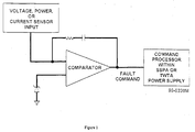
- FIG. 1 is a schematic diagram of a typical protection circuit that is susceptible to single event phenomenon.
- This figure shows a typical electronic protection circuit that is susceptible to SEU.
- This versatile circuit has applications for many common circuit conditions, including by way of example, power-on reset, over current protection , and overpower or over voltage protection . Commonly, these conditions result in a shut off the power supply to a circuit, or a power-on reset for digital components so as to protect the rest of the electronic components.
- the protection circuit is typically based on fast-acting comparator such as LM139 or other similar devices. This is because the circuit protection or circuit shut off has to occur almost instantaneously ( ⁇ 5 microseconds) in order to provide required protection.
- the present invention utilizes a combination of an additional comparator in conjunction with a logic family device gate (e.g., NAND or NOR).
- a logic family device gate e.g., NAND or NOR.
- This configuration mitigates a circuit's single event effects ('SEE") and makes the design immune to SEU phenomenon.
- the illustrated embodiment uses a second comparator and combines the outputs from both comparator devices using a NAND gate or a NOR gate. This insures that a false signal can only occur if both comparators are upset simultaneously. This is due to the nature of the operation of digital logic devices, which provide an output only when both inputs are "low” (NOR gates) or "high” (NAND gate) - see logic Tables 1 and 2 below.
- Figure 1 was susceptible to frequent upsets.
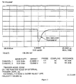
- Figure 2 is a waveform that graphically depicts a typical response of the tested semiconductor device. Such response, in its actual application, would result in unacceptable hardware performance.
- frequent upsets were observed at the output of each of the individual devices for the modified circuits.
- Figure 3 includes waveforms depicting the effect of cosmic rays on the common device shown in Figure 4. More particularly, Figure 3 shows the simultaneous response of four devices in the same package when exposed to cosmic rays. It demonstrates that no two devices were upset simultaneously, thus insuring that the inputs to the logic family device do not change state as a result of SEU event. This demonstrates that circuits in accordance with the present invention are immune to single event upsets.
- comparator typically come with 4 devices per single package a shown in Figure 4.
- most designs usually have redundant devices such as LM139 or NAND gates already available on a typical circuit board.
- NOR and NAND gates from various vendors are themselves immune to single event upset. Two implementations of such circuit are shown in Figures 5 and 6.
- the values of ⁇ and L are 4.3x10 -4 and 8, respectively.
- the upset rate of the modified circuit is R ⁇ 10 -5 upsets/device/year or less than one upset per 1,000 years.
- the values of ⁇ and L are ⁇ 10 -6 and 83, respectively.
- Logic gate input terminals are in either High or Low state by applying appropriate voltages to them; then the output terminals are in High or Low state, depending on the logic function performed. Only two voltage levels are allowed at the terminals of digital logic gates -- one that represents a "Low” voltage, and one that represents a "High” voltage.
- truth table which relates the voltage level at the output terminal to the voltage levels at the input terminals.
- the truth table for a NOR gate is given below.
- the output of a NOR gate is Low when input A or B (or both) is High.
- the output is High when inputs A and B are Low.
- the single event upset circuit shown in Figure 5 and its operation is described below.
- the basic function of the NOR gate is as follows. For protection circuits that are configured such that in the normal condition both comparator outputs are High and no signal is generated at the output of the circuit at the NOR gate (output is Low). For this circuit, the indication of the true fault condition would by high state at the output of the NOR gate. If any of the two comparators are upset by SEU such that it's output goes Low, this has no impact on the NOR gate output because second comparator output is still high since the do not upset simultaneously. In case of true fault condition, both comparator output are puled low and NOR gate output changes state to High, issuing the True Fault signal.
- the operation of the circuit shown in Figure 6 is described below.
- the basic function of the NAND gate is as follows. For protection circuits that are configured such that in the normal condition both comparator outputs are Low and signal is generated at the output of the circuit at the NAND gate (output is High) indicating No Fault condition. For this circuit, the indication of the true fault condition would by Low state at the output of the NAND gate. If any of the two comparators is upset by SEU such that it's output goes High, this has no impact on the NAND gate output because the second comparator output is still high since both of them do not upset simultaneously. In case of true fault condition, both comparator outputs are puled High and NAND gate output changes state to Low, issuing the True Fault signal.
- the above describes a novel approach to protecting and mitigating the effects of single event upsets due to, for example, cosmic rays.
- the present invention insures single event upset immunity of a circuit design, and will prevent uncommanded on-orbit cosmic ray-induced shut offs of protected circuits and equipment. Consequently, in the case of utilizing the present invention in spacecraft, the loss of communications traffic and associated revenue losses can be eliminated.
Landscapes
- Physics & Mathematics (AREA)
- Engineering & Computer Science (AREA)
- Computer Hardware Design (AREA)
- Computing Systems (AREA)
- General Engineering & Computer Science (AREA)
- Mathematical Physics (AREA)
- Logic Circuits (AREA)
- Hardware Redundancy (AREA)
Abstract
Description
LET is in MeV.cm2/mg.
| Truth table for a NOR gate | ||
| A | B | C |
| Low | Low | High |
| Low | High | Low |
| High | Low | Low |
| High | High | Low |
| Truth table for a NAND gate | ||
| A | B | C |
| Low | Low | High |
| Low | High | High |
| High | Low | High |
| High | High | Low |
Claims (7)
- A single event upset mitigation circuit comprising:a first circuit including a first output with normal and fault states;a second circuit including a second output with normal and fault states; anda logic gate including a first input operatively coupled to the first output and a second input operatively coupled to the second output, and including an output having a fault state when the first and second outputs are the fault state.
- A single event upset mitigation circuit according to claim 1, wherein the first and second circuits comprise respective comparators.
- A single event upset mitigation circuit according to claim 1 or 2, wherein the logic gate comprises an NAND logic gate.
- A single event upset mitigation circuit according to claim 1 or 2, wherein the logic gate comprises a NOR logic gate.
- A method of mitigating single event upset in first and second circuits having respective outputs with normal and fault states, comprising:receiving an output from the first circuit;receiving an output from the second circuit;comparing the outputs of the first and second circuits; andproviding a fault output only when the outputs of the first and second circuits are the fault state.
- A method of mitigating single event upset according to claim 5, wherein the comparing includes performing a logical NAND operation on the outputs of the first and second circuits.
- A method of mitigating single event upset according to claim 5, wherein the comparing includes performing a logical NOR operation on the outputs of the first and second circuits.
Applications Claiming Priority (2)
| Application Number | Priority Date | Filing Date | Title |
|---|---|---|---|
| US58680600A | 2000-06-05 | 2000-06-05 | |
| US586806 | 2000-06-05 |
Publications (2)
| Publication Number | Publication Date |
|---|---|
| EP1170866A2 true EP1170866A2 (en) | 2002-01-09 |
| EP1170866A3 EP1170866A3 (en) | 2002-01-16 |
Family
ID=24347172
Family Applications (1)
| Application Number | Title | Priority Date | Filing Date |
|---|---|---|---|
| EP01304680A Withdrawn EP1170866A3 (en) | 2000-06-05 | 2001-05-30 | Comparator with duplex architecture for single event upset protection |
Country Status (2)
| Country | Link |
|---|---|
| EP (1) | EP1170866A3 (en) |
| CA (1) | CA2348200A1 (en) |
Families Citing this family (2)
| Publication number | Priority date | Publication date | Assignee | Title |
|---|---|---|---|---|
| CN113014312B (en) * | 2018-06-08 | 2022-09-27 | 上海微小卫星工程中心 | Protection and fault processing method for dealing with space particle effect |
| CN118688598B (en) * | 2024-06-03 | 2025-10-03 | 安徽大学 | Single event upset fault injection method and platform |
Family Cites Families (6)
| Publication number | Priority date | Publication date | Assignee | Title |
|---|---|---|---|---|
| US3075153A (en) * | 1958-08-18 | 1963-01-22 | Gen Dynamics Corp | Redundant amplifier |
| US3219913A (en) * | 1963-05-17 | 1965-11-23 | Brown Irving | Automatic maintenance circuit |
| US3614401A (en) * | 1969-04-01 | 1971-10-19 | Rosemount Eng Co Ltd | Redundant system |
| US5031180A (en) * | 1989-04-11 | 1991-07-09 | Trw Inc. | Triple redundant fault-tolerant register |
| US6133747A (en) * | 1997-07-22 | 2000-10-17 | University Of New Mexico | Time redundant radiation tolerant logic |
| US6252433B1 (en) * | 1999-05-12 | 2001-06-26 | Southwest Research Institute | Single event upset immune comparator |
-
2001
- 2001-05-18 CA CA 2348200 patent/CA2348200A1/en not_active Abandoned
- 2001-05-30 EP EP01304680A patent/EP1170866A3/en not_active Withdrawn
Also Published As
| Publication number | Publication date |
|---|---|
| CA2348200A1 (en) | 2001-12-05 |
| EP1170866A3 (en) | 2002-01-16 |
Similar Documents
| Publication | Publication Date | Title |
|---|---|---|
| Guenzer et al. | Single event upset of dynamic RAMs by neutrons and protons | |
| Lesea et al. | The rosetta experiment: atmospheric soft error rate testing in differing technology FPGAs | |
| Koga et al. | On the suitability of non-hardened high density SRAMs for space applications | |
| US6046606A (en) | Soft error protected dynamic circuit | |
| US20080158747A1 (en) | Radiation tolerant electrostatic discharge protection networks | |
| Campbell et al. | Single event upset rates in space | |
| Baumann | Soft errors in commercial integrated circuits | |
| JP2008543179A (en) | Single event effect enhancement circuit | |
| Vampola | Thick dielectric charging on high-altitude spacecraft | |
| US20060119410A1 (en) | Pulse-rejecting circuit for suppressing single-event transients | |
| Wang et al. | Soft error rate determination for nanometer CMOS VLSI logic | |
| JP5159057B2 (en) | Method and system for reducing transient event effects within an electrostatic discharge power clamp | |
| US7489538B2 (en) | Radiation tolerant combinational logic cell | |
| LaBel et al. | Transient SEUs in a fiber optic system for space applications | |
| CA2348200A1 (en) | Mitigating single event upset phenomenon in semiconductor circuits | |
| JP2007189191A (en) | Single event transient immunity antenna diode circuit | |
| Saxena et al. | Single event upset (SEU) in SRAM | |
| Castano et al. | Impact of radiation on electronics | |
| Rasmussen | Spacecraft electronics design for radiation tolerance | |
| Dicello | Microelectronics and microdosimetry | |
| Nichols et al. | Device SEE susceptibility from heavy ions (1995-1996) | |
| KR20230063394A (en) | Pulsed radiation protection module with timing control function | |
| Ki et al. | Dual-Sensor-Based Active Protector for Nuclear EMP and Prompt Gamma-Ray Detection | |
| KR102962632B1 (en) | Nuclear PR, NEMP and non-nuclear NNEMP multi-protection devices with error filtering circuitry | |
| US7466181B2 (en) | Dose rate event protection clamping circuit |
Legal Events
| Date | Code | Title | Description |
|---|---|---|---|
| PUAI | Public reference made under article 153(3) epc to a published international application that has entered the european phase |
Free format text: ORIGINAL CODE: 0009012 |
|
| PUAL | Search report despatched |
Free format text: ORIGINAL CODE: 0009013 |
|
| AK | Designated contracting states |
Kind code of ref document: A2 Designated state(s): AT BE CH CY DE DK ES FI FR GB GR IE IT LI LU MC NL PT SE TR Kind code of ref document: A2 Designated state(s): DE FR GB IT |
|
| AX | Request for extension of the european patent |
Free format text: AL;LT;LV;MK;RO;SI |
|
| AK | Designated contracting states |
Kind code of ref document: A3 Designated state(s): AT BE CH CY DE DK ES FI FR GB GR IE IT LI LU MC NL PT SE TR |
|
| AX | Request for extension of the european patent |
Free format text: AL;LT;LV;MK;RO;SI |
|
| 17P | Request for examination filed |
Effective date: 20020710 |
|
| AKX | Designation fees paid |
Free format text: DE FR GB IT |
|
| GRAH | Despatch of communication of intention to grant a patent |
Free format text: ORIGINAL CODE: EPIDOS IGRA |
|
| STAA | Information on the status of an ep patent application or granted ep patent |
Free format text: STATUS: THE APPLICATION IS DEEMED TO BE WITHDRAWN |
|
| 18D | Application deemed to be withdrawn |
Effective date: 20030514 |