EP1170791A2 - Semiconductor device with multilayer wiring structure of laminated damascene wiring and fabrication method thereof - Google Patents
Semiconductor device with multilayer wiring structure of laminated damascene wiring and fabrication method thereof Download PDFInfo
- Publication number
- EP1170791A2 EP1170791A2 EP01114349A EP01114349A EP1170791A2 EP 1170791 A2 EP1170791 A2 EP 1170791A2 EP 01114349 A EP01114349 A EP 01114349A EP 01114349 A EP01114349 A EP 01114349A EP 1170791 A2 EP1170791 A2 EP 1170791A2
- Authority
- EP
- European Patent Office
- Prior art keywords
- film
- wiring
- forming
- dielectric film
- semiconductor device
- Prior art date
- Legal status (The legal status is an assumption and is not a legal conclusion. Google has not performed a legal analysis and makes no representation as to the accuracy of the status listed.)
- Withdrawn
Links
Images









Classifications
-
- H—ELECTRICITY
- H10—SEMICONDUCTOR DEVICES; ELECTRIC SOLID-STATE DEVICES NOT OTHERWISE PROVIDED FOR
- H10W—GENERIC PACKAGES, INTERCONNECTIONS, CONNECTORS OR OTHER CONSTRUCTIONAL DETAILS OF DEVICES COVERED BY CLASS H10
- H10W20/00—Interconnections in chips, wafers or substrates
- H10W20/01—Manufacture or treatment
- H10W20/031—Manufacture or treatment of conductive parts of the interconnections
- H10W20/062—Manufacture or treatment of conductive parts of the interconnections by smoothing of conductive parts, e.g. by planarisation
-
- H—ELECTRICITY
- H10—SEMICONDUCTOR DEVICES; ELECTRIC SOLID-STATE DEVICES NOT OTHERWISE PROVIDED FOR
- H10W—GENERIC PACKAGES, INTERCONNECTIONS, CONNECTORS OR OTHER CONSTRUCTIONAL DETAILS OF DEVICES COVERED BY CLASS H10
- H10W20/00—Interconnections in chips, wafers or substrates
- H10W20/01—Manufacture or treatment
- H10W20/031—Manufacture or treatment of conductive parts of the interconnections
- H10W20/056—Manufacture or treatment of conductive parts of the interconnections by filling conductive material into holes, grooves or trenches
-
- H—ELECTRICITY
- H10—SEMICONDUCTOR DEVICES; ELECTRIC SOLID-STATE DEVICES NOT OTHERWISE PROVIDED FOR
- H10W—GENERIC PACKAGES, INTERCONNECTIONS, CONNECTORS OR OTHER CONSTRUCTIONAL DETAILS OF DEVICES COVERED BY CLASS H10
- H10W20/00—Interconnections in chips, wafers or substrates
- H10W20/01—Manufacture or treatment
- H10W20/071—Manufacture or treatment of dielectric parts thereof
- H10W20/081—Manufacture or treatment of dielectric parts thereof by forming openings in the dielectric parts
Definitions
- the present invention relates to a semiconductor device that is provided with a multilayer wiring structure with laminated damascene wiring, and to a method of fabricating such a semiconductor device.
- tungsten and copper are used for filling these contact holes and via-holes.
- CVD Chemical Vapor Deposition
- plating the film is planarized by, for example, CMP (Chemical Mechanical Polishing), whereby the conductive film is embedded inside the holes to form via-plugs.
- CMP Chemical Mechanical Polishing
- a cavity referred to as a "seam" occurs at the center line of the plug, and this cavity can cause various problems in processing. This point will be explained below using a method of the prior art for fabricating a tungsten plug as an example.
- damascene copper wiring is formed as shown in Fig. 1A.
- silicon oxide film 1, silicon oxynitride film 2, and silicon oxide film 3 are formed by a plasma CVD method on a semiconductor substrate 100 on which, for example, transistors (not shown in the figure) are formed. Copper film 5 is then embedded in silicon oxide film 3 by a known damascene method to form copper wiring. Silicon nitride film 6 and silicon oxide film 7 are then formed on this structure by, for example, plasma CVD. Resist film 8 having a prescribed opening is next provided on silicon oxide film 7. Using this film as a mask, silicon oxide film 7 is then subjected to dry etching to form a via-hole that reaches silicon nitride film 6 (Fig. 1B). Oxygen plasma ashing is then carried out to remove resist film 8.
- the resist residue that adheres to the surface of silicon oxide film 7 and the inner walls of the hole is then removed by a resist removing solution (Fig. 1C).
- Silicon nitride film 6 is then subjected to dry etching to expose the surface of wiring film 5.
- the resist residue is then removed by a resist removing solution (Fig. 1D).
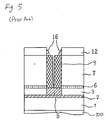
- tungsten film 9 is formed over this adhesive film using CVD (Fig. 2A). After forming tungsten film 9, the film is planarized using CMP processing solution 11 to form tungsten film 9 inside the via-hole (Fig. 2B). At this time, a seam occurs within tungsten film 9. The mechanism of the occurrence of this seam will be next briefly explained.
- the thickness of the tungsten film that adheres to the inner walls of the via-hole is thin in the initial stages of the film growth, and film growth proceeds smoothly because the inside of the hole can be easily supplied with the material gas.
- tungsten film 9 becomes more thickly deposited on the inner walls of the hole, however, the space in the hole gradually shrinks, and the supply of the material gas to the hole interior is impeded.
- the rate of film growth of tungsten film 9 inside the hole decreases as the space inside the hole shrinks, and the rate of film growth is considered to approach 0 in the final stages of the embedding, whereby the cavity that is referred to as a seam occurs in tungsten film 9. Owing to the above-described mechanism of their occurrence, many seams occur particularly when forming plugs having a high aspect ratio.
- silicon oxide film 12 is formed on tungsten film 9 by a CVD method (Fig. 3A).
- Resist film 14 having a prescribed opening is then provided (Fig. 3B).
- a wiring trench is formed in silicon oxide film 12 (Fig. 3C).
- An oxygen plasma ashing process and a stripping process using removing solution are carried out to remove resist film 14 and etching residue. At this time, removing solution 15 penetrates the seam in the tungsten film as shown in Fig. 4A.
- Copper film 16 is then formed over the entire surface (Fig. 4B), and during the film formation or the subsequent annealing process, removing solution 15 vaporizes, expands in volume, and causes a blister in copper film 16 (Fig. 4C).
- Figs. 6A-8B show the steps of forming a plug according to a second example of the prior art.
- a wiring structure is formed in which a tungsten plug is provided between copper wiring.
- silicon oxide film 1 and silicon oxynitride film 2 are first formed by plasma CVD.
- HSQ (hydrogen silisesquioxane) film 33 is then formed by a rotational application method, following which copper film 5 is embedded in HSQ film 33 by a known damascene method to form copper wiring.
- Silicon nitride film 6 and silicon oxide film 7 are then formed over copper layer 5 and HSQ film 33 by a plasma CVD method.
- a via-plug composed of tungsten film 9 is then formed by the same procedure as in the first example of the prior art.
- Silicon oxynitride film 35 and HSQ film 33 are then formed over tungsten film 9.
- resist film 30 having a prescribed opening is provided over silicon oxynitride film 35 and HSQ film 33.
- Fig. 6A shows the state following completion of the above-described processes.
- an opening is formed in HSQ 33 and silicon oxynitride film 35 by dry etching to expose tungsten film 9 (Fig. 6B). Ashing and a stripping process using a resist removing solution are then carried out to remove resist 30.
- a solution having a strong removing action such as ammonium fluoride is used as the removing solution.
- the removing solution is selected as appropriate according to processing conditions such as the ashing conditions, the material to be etched in the etching of wiring trenches, and the etching gas.
- a low-corrosion amine removing solution containing corrosion inhibitors is used, as in the first example of the prior art.
- Fig. 6C shows the subsequent state of completion of the upper copper wiring by forming copper film 16.
- metal corrosion area 20 results in an increase in contact resistance and wiring resistance and a large-scale reduction of element characteristics.
- a removing solution having low corrosion against metal may be used to suppress the occurrence of metal corrosion area 20 as previously described, but some processes compel the use of a strong removing solution to remove etching deposits. In such cases, an effective means of avoiding the above-described problem of corrosion has yet to be found.
- CMP process solution 11 that remains in the seam that occurs in tungsten film 9 may result in a blister in the film during the process of heating and curing HSQ film 33 after forming silicon oxynitride film 35 and HSQ film 33 as shown in Fig. 8B.
- CMP processing solution 11 in a seam may vaporize and thus become removable when forming silicon oxynitride film 35, but removing the remaining liquid for all via-plugs that are formed on a wafer is problematic.
- silicon oxynitride film 35 may be formed before all remaining liquid is eliminated, and the above-described problem becomes conspicuous.
- Defects may also occur in the formation of a conductive film inside a via-hole before the occurrence of a seam.
- the tungsten may be deposited in an overhanging state at the upper portion of the hole and thus cause a void-shaped cavity to occur inside the hole.
- problems such as blistering or peeling of a film or corrosion of wiring may occur as in the case of the occurrence of a seam.
- An object of the present invention is to provide such a process and a method that prevents blistering of a film or peeling of a film in cases in which CMP polishing solution, rinsing solution, or resist removing solution is present inside a cavity and that enables the fabrication of high-quality semiconductor devices at high product yield.
- the first method of the present invention that solves the above-described problems is as follows:
- An interlayer dielectric film is formed on a semiconductor substrate, following which a depression is formed in the interlayer dielectric film.
- a first conductive film is embedded in the depression by depositing a conductive material over the entire surface of the interlayer dielectric film so as to bury the depression and then removing the conductive material from areas other than the depression.
- a heat treatment is performed to dry the interior of cavities that have occurred in the first conductive film.
- a second conductive film is formed that contacts the upper surface of the first conductive film.
- the second method of the present invention is as follows:
- Lower-layer wiring is formed on a dielectric film that is provided on a semiconductor substrate, following which an interlayer dielectric film is formed over the entire surface of the lower-layer wiring and the dielectric film.
- Connection holes are provided in the interlayer dielectric film that reach the lower-layer wiring and a metal film is formed over the entire surface of the interlayer dielectric film, following which the metal film is removed until the surface of the interlayer dielectric film is exposed to form wiring plugs inside the connection holes.
- a heat treatment is performed to dry the interior of cavities that have occurred in the wiring plugs.
- Upper-layer wiring is formed that connects to the wiring plugs.
- the interiors of the cavities of seams or voids that have occurred in a conductive film of interlayer connection plugs or damascene wiring are first dried before forming another overlying film.
- the occurrence of blistering or peeling of a film due to the expansion of liquids such as CMP processing solution or resist removing solution that are present inside the cavities can be prevented.
- the method of the present invention can further prevent problems such as the corrosion of an underlying conductive film by liquid that remains inside a seam.
- the method of the present invention enables fabrication of high-quality semiconductor devices at good product yield.
- the third method of the present invention is as follows:
- a first conductive film is formed on a semiconductor substrate, an interlayer dielectric film is formed on this first conductive film, following which a first depression is formed in the interlayer dielectric film.
- a second conductive film is embedded inside the depression by depositing a conductive material over the entire surface of the interlayer dielectric film so as to bury the first depression and then removing the deposited conductive material in areas other than the depression.
- a dielectric material is applied to cavities that have occurred in the second conductive film and to the upper portion of the second conductive film using a rotational application method and then dried to form a dielectric film.
- the dielectric film is etched to form a second depression in which the second conductive film is exposed at the bottom, following which a third conductive film is formed to bury the second depression.
- the fourth method of the present invention is as follows:
- Lower-layer wiring is formed on a dielectric film that is provided on a semiconductor substrate, following which an interlayer dielectric film is formed over the entire surface of the lower-layer wiring and the dielectric film.
- Connection holes that reach to the lower-layer wiring are provided in the interlayer dielectric film and a metal film is formed over the entire surface of the interlayer dielectric film, following which the metal film is removed until the surface of the interlayer dielectric film is exposed to form wiring plugs in the connection holes.
- a dielectric material is applied to cavities that occur in the wiring plugs and to the upper portion of the wiring plugs using a rotational application method and then dried to form a dielectric film.
- the dielectric film is etched to form wiring trenches in which the wiring plugs are exposed at the bottom, following which upper-layer wiring is formed to bury the wiring trenches.
- a rotational application dielectric material i.e., a material that allows a solution that contains a dielectric film material to be applied by rotational application method, is preferably used as the dielectric material in these methods.
- the semiconductor device of the present invention is provided with a first conductive film and a second conductive film that is formed in contact with the upper surface of the first conductive film on a semiconductor substrate, wherein a dielectric material is embedded in cavities in the first conductive film.
- Another semiconductor device of the present invention is provided with lower-layer wiring that is formed on a semiconductor substrate, upper-layer wiring that is formed over the lower-layer wiring, and wiring plugs that connect the wiring, wherein a dielectric material is embedded in cavities in the wiring plugs.
- a rotational application material i.e., a material that allows a solution containing a dielectric film material to be applied by rotational application method, is preferably used as the dielectric material.
- An inorganic polysiloxane such as HSQ, a polyorganosiloxane such as MHSQ or MSQ (methyl silisesquioxane), or an aromatic organic resin such as polyarylene ether (PAE) or divinyl siloxane-bis-benzocyclobutene (BCB) can be used as the rotational application material.
- PAE polyarylene ether
- BCB divinyl siloxane-bis-benzocyclobutene
- the semiconductor device fabrication method of the present invention can take the form of, for example, a method including the following steps.
- cavities may be buried by a rotational application dielectric material following the drying step.
- Step (b) may be realized by Chemical Mechanical Polishing (CMP).
- CMP Chemical Mechanical Polishing
- the lower-layer wiring and upper-layer wiring may be composed by copper or a copper alloy, and the connection plugs may be composed by tungsten.
- the first, second, and third conductive films may each be wiring films that are formed by a dual-damascene method.
- the method of forming the first, second, and third conductive films is not specifically limited, but is preferably a film formation method that enables films to be effectively embedded.
- the second conductive film is preferably formed by CVD.
- the drying step is preferably performed between Step (b) and Step (c), or between Step (f) and Step (g). If the drying step is performed between Steps (b) and (c), fluids (CMP polishing solution or rinse solution) used in Step (b) that remain inside cavities of the second conductive film can be vaporized. If the drying step is performed between Steps (f) and (g), resist removing solution that remains inside cavities of the second conductive film can be vaporized. Because remaining resist removing solution can bring about such adverse effects as damage to the first conductive film, the employment of the drying step between Steps (f) and (g) is particularly effective.
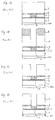
- damascene copper wiring is first formed.
- silicon oxide film 1, silicon oxynitride film 2, and silicon oxide film 3 are formed by, for example, plasma CVD on a semiconductor substrate 100 on which transistors (not shown) have been formed. Copper film 5 is then embedded in silicon oxide film 3 by a known damascene method to form the copper wiring. Next, silicon nitride film 6 and silicon oxide film 7 are formed over silicon oxide film 3 and copper film 5 by, for example, a plasma CVD method.
- Resist film 8 having a prescribed opening is next provided on silicon oxide film 7, and using this resist film 8 as a mask, silicon oxide film 7 is subjected to dry etching to form a via-hole that reaches as far as silicon nitride film 6 (Fig. 9B).
- resist residue that adheres to the surface of silicon oxide film 7 and to the inner walls of the hole is removed by a resist removing solution (Fig. 9C).
- Silicon nitride film 6 is next subjected to dry etching to expose the surface of copper film 5, following which the resist residue is removed by a resist removing solution (Fig. 9D).
- an adhesive film (not shown in the figure) is formed over the entire surface of silicon oxide film 7.
- the adhesive film is formed to strengthen adhesion between tungsten and the inner walls of the via-hole, and may be a film in which, for example, a titanium film and a titanium nitride are laminated in that order.
- the titanium film is formed by a sputtering and may have a thickness of, for example, 20-50 nm.
- the titanium nitride film is formed by, for example, a reactive sputtering and has a thickness of, for example, 20-50 nm.
- the adhesive film that is composed of these films strengthen adhesion between the interlayer dielectric film and the tungsten film that is formed in the next step.
- Tungsten film 9 is then formed by CVD on the adhesive film (Fig. 10A).
- the material gas when forming the film is, for example, a gas containing WF 6 .
- the interior of the via-hole is thus buried by tungsten.
- Tungsten film 9 can be formed in a variety of CVD conditions.
- tungsten film 9 can be formed by first lightly forming tungsten micro-crystals, which are the nuclei for forming a high-density CVD tungsten film, on the inner surfaces of the hole and growing the crystals by low-pressure CVD (growth nucleus formation step), and then carrying out a bulk tungsten film formation step.
- a tungsten film that is relatively well-suited for embedding can be formed by adopting this type of film formation process, complete suppression of the occurrence of seams is difficult.
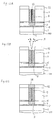
- CMP is carried out using a slurry containing an oxidizing agent and an abrasive, followed by rinsing with pure water. Excess tungsten film 9 that has formed outside the hole is thus removed and a via-plug composed of tungsten film 9 inside the via-hole is formed (Fig. 10B). At this time, CMP processing solution 11 that is made up by CMP polishing solution and rinse solution penetrates the seams that have occurred in tungsten film 9.
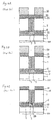
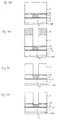
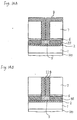
- Silicon oxide film 12 is next formed on tungsten film 9 (Fig. 11A). Silicon oxide film 12 is formed by plasma CVD using, for example, monosilane or TEOS (tetraethoxysilane) as the material gas. Although silicon oxide film 12 is formed directly on tungsten film 9 in the present embodiment, a silicon nitride film may be interposed between these films. After forming silicon oxide film 12, resist film 14 having prescribed openings is provided (Fig. 11B), and wiring trenches are formed in silicon oxide film 12 using this resist film 14 as a mask (Fig. 11C).
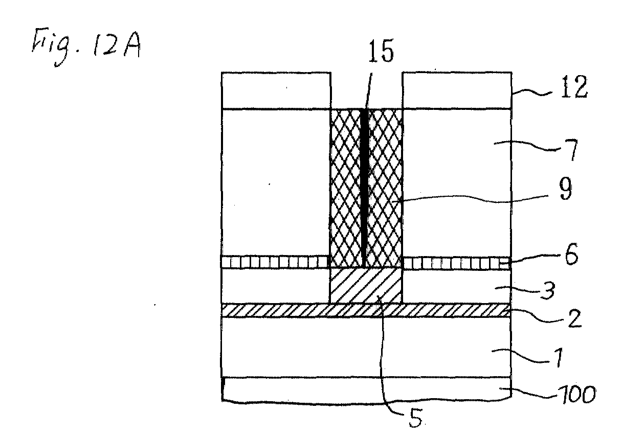
- Oxygen plasma ashing and processing by an amine removing solution are next carried out to remove resist film 14 and the etching residue.
- amine removing solution 15 penetrates the seam in the tungsten film as shown in Fig. 12A.
- a heat treatment is carried out to vaporize this amine removing solution 15 (Fig. 12B).
- the temperature of the heat treatment is preferably 200-450°C, and more preferably 350-450°C. If the temperature of the heat treatment is too low, removing solution will remain, and this will give rise to blistering or peeling of the wiring that is formed on the tungsten plug and cause damage to the wiring composed of copper film 5. Making the temperature of the heat treatment too high, on the other hand, may affect the distribution of the impurity diffusion layer or adversely affect element performance.
- the duration of the heat treatment is preferably greater than one minute, and more preferably greater than 10 minutes. The interiors of seams can thus be dried sufficiently. Although there is no particular limitation on the maximum duration, a process of 30 minutes or less is sufficient. Examples of preferable heat treatment conditions are given below:
- seam interior can be more adequately dried using the conditions in case (i). Copper film 16 is then embedded in the wiring trenches by a known damascene process to form damascene copper wiring (Fig. 12C). According to the processes shown in the present embodiment, seam interiors are sufficiently dried by the heat treatment of Fig. 12B, and the occurrence of blistering in copper film 16 that is formed above the seam can therefore be suppressed and a wiring structure of higher reliability can be formed at a high product yield.
- This embodiment is a case in which HSQ, which is one type of rotational application dielectric material, is used as the material of the interlayer dielectric film of the copper wiring layers.
- silicon oxide film 1, silicon oxynitride film 2, HSQ film 33, and copper film 5 are formed on a semiconductor substrate to form damascene copper wiring, following which tungsten film 9 is formed inside a via-hole in silicon nitride film 6 and silicon oxide film 7 so as to contact the copper wiring.
- HSQ 33 is formed by a rotational application method.
- the film is formed by applying, to the surface of a wafer that is rotating at a prescribed speed, a solution containing the HSQ film material as a liquid, and then carrying out a multi-stage heat treatment.
- An example of the conditions for rotational application method is as follows:
- HSQ film 33 which has a low dielectric constant, as the dielectric film of the copper wiring layer suppresses the occurrence of interwiring crosstalk and improves the high-speed operation of the elements.
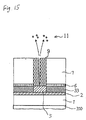
- a heat treatment is carried out to vaporize CMP process solution 11 composed of the CMP polishing solution and rinse solution that has entered the seam (Fig. 15).
- the temperature of the heat treatment is preferably 200-450°C, and more preferably 350-450°C.
- the duration of the heat treatment is preferably one minute or greater, and more preferably 10 minutes or greater.
- the seam interior can thus be adequately dried. Although there is no limitation on the maximum duration, a process of 30 minutes or less is adequate. Examples of preferable heat treatment conditions are shown below:
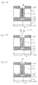
- HSQ film 33 is next formed directly on tungsten film 9 by a rotational application method (Fig. 16A). HSQ film 33 is formed by a rotational application method.
- An example of the conditions for rotational application method is as follows:
- Figs. 16B-17C are next carried out similar to the steps shown in Figs. 11B-12C of the first embodiment.
- a heat treatment is carried out to vaporize amine removing solution 15.
- the preferable heat treatment conditions are the same as those described in the explanation of Fig. 12B.
- the wiring structure is formed by proceeding through the above-described steps.
- a rotationally applied film such as HSQ as the dielectric film of the wiring layer can both suppress the occurrence of crosstalk and improve flatness
- the temperature of film formation is close to room temperature and chemical solutions such as the CMP process solutions therefore tend to remain in seams.
- a heat treatment is therefore performed before forming the HSQ film over the tungsten plug in the present embodiment.
- seam interiors are adequately dried by a heat treatment and the occurrence of blistering in the overlying HSQ film or copper film can therefore be suppressed, whereby a wiring structure having high reliability can be formed with good product yield.
- This embodiment is a case in which methyl hydrogen silisesquioxane (hereinbelow referred to as "MHSQ"), which is one type of rotationally applied film material, is used as the material of the interlayer dielectric film of the copper wiring layers.
- MHSQ methyl hydrogen silisesquioxane
- the present embodiment is a process similar to the second embodiment but differs in that an ammonium fluoride removing solution having a strong removing action is employed as the resist removing solution and a film having a low dielectric constant is caused to partially enter the seams.
- silicon oxide film 1, silicon oxynitride film 2, MHSQ film 17, and copper film 5 are formed on a semiconductor substrate to form damascene copper wiring, following which tungsten film 9 is formed in via-holes in silicon nitride film 6 and silicon oxide film 7 so as to contact the copper wiring.
- MHSQ film 17 is formed by a rotational application method. The conditions of this film formation are shown below:
- MHSQ film 17 is formed directly on tungsten film 9 (Fig. 18A).
- MHSQ film 17 is formed by a rotational application method, and conditions are selected such that MHSQ material enters the seams. For this purpose, it is effective to carry out a first application while rotating the wafer at a low speed and then carrying out a second application while rotating the wafer at a high speed.
- An example of these rotational application conditions is shown below:
- MHSQ film can also be embedded inside seams as shown in Fig. 18A.
- Resist film 10 is then formed, and using this film as a mask, MHSQ film 17 is dry etched to form wiring trenches (Figs. 18B and 18C). An ashing process and a removing process using ammonium fluoride removing solution are then carried out to remove resist film 10 (Fig. 19A).
- etching is carried out to form wiring trenches, etching deposits that are difficult to remove normally adhere to the inner walls of trenches and the side walls of resist film 10. A removing solution having strong removing action is used in this embodiment and these etching deposits can therefore be effectively removed.
- the embedding of MHSQ film 17 in seams that occur in tungsten film 9 prevents removing solution from reaching and corroding the surface of silicon nitride film 6.
- Copper film 16 is then formed inside the wiring trenches provided in MHSQ film 17, and the wiring structure in which lower-layer and upper-layer copper wiring are connected by a tungsten plug is completed (Fig. 19B).
- the present invention can also be applied to steps for forming copper wiring.
- the present invention is also effective for vaporizing liquids that remain in seams that occur in copper wiring by a heat treatment and preventing blistering of films that are formed over the seams.
- the present invention is also effective when applied to a process that employs copper as the plug material.
- plating solution may remain in seams when a copper film is formed by plating, and the process of the present invention can be effectively applied to removing this plating solution.
- the two-layer wiring structure shown in Fig. 20 was fabricated according to the process described in the third embodiment and a test of reliability was performed.
- This two-layer wiring structure is referred to as a "via-chain,” and is provided with 15,000 parallel lower-layer copper lines made up by copper film 5 and 15,000 parallel upper-layer copper lines made up by copper film 16 that are orthogonal to lower-layer copper lines 5.
- This wiring is interconnected by 30,000 via-plugs composed of tungsten film 9.
- the semiconductor substrate and interlayer dielectric film have been omitted.
- the inside diameters of the via-holes were as follows:
- silicon oxide film 1, silicon oxynitride film 2, MHSQ film 17 (instead of HSQ film 33), and copper film 5 were formed on a semiconductor substrate to form damascene copper wiring, following which tungsten film 9 was formed in via-holes in silicon nitride film 6 and silicon oxide film 7 so as to connect to the copper wiring.
- Copper film 5 was formed by a plating process and had a wiring width of 0.3 ⁇ and a wiring thickness of 350 nm.
- MHSQ film 17 was formed by rotational application method of an MHSQ solution.
- the MHSQ film formation was performed at room temperature (approximately 25°C), the speed of wafer rotation during application was 1500 rpm (one-stage application), and curing was performed as a three-stage process at 80°C, 100°C, and 120°C.
- MHSQ film 17 was formed directly on tungsten film 9 by rotational application method (Fig. 18A). MHSQ film 17 was formed by rotational application method.
- the rotational application conditions were as follows:
- MHSQ film 17 was subjected to dry etching using this resist film 10 as a mask to form wiring trenches (Figs. 18B and 18C), following which an ashing process and a removing process using an ammonium fluoride removing solution were carried out to remove resist film 10 (Fig. 19A).
- Copper film 16 was then formed and CMP was performed to form a wiring structure in which lower-layer and upper-layer copper wiring were connected by tungsten plugs (Fig. 19B).
- FIG. 21 A plurality of chips provided with the wiring structures of working examples 1-3 according to the above-described processes were fabricated and the chain resistance was measured. The results of this test are shown in Fig. 21.
- the horizontal axis shows the wiring resistance per one via-hole
- the vertical axis shows the cumulative probability. All of the wiring structures obtained by the present working examples exhibited low resistance.
- FIG. 20 A two-layer wiring structure shown in Fig. 20 was fabricated in accordance with processes (Figs. 6A-8B) according to the second example of the prior art that was described in the prior art section, and the reliability of the structure was tested.
- This structure differs from working examples 1-3 in that the step of drying seams was not carried out and silicon oxynitride film 35 was provided over the tungsten plugs.
- the processes employed were otherwise the same as for working examples 1-3.
- the inner diameters of the via-holes were as follows:
Landscapes
- Internal Circuitry In Semiconductor Integrated Circuit Devices (AREA)
Abstract
Description
Figs. 6A-8B show the steps of forming a plug according to a second example of the prior art. First, as shown in Fig. 6A, a wiring structure is formed in which a tungsten plug is provided between copper wiring.
In addition, the first, second, and third conductive films may each be wiring films that are formed by a dual-damascene method.
(approximately 25°C)
1500 rpm (one-stage application)
After forming a via-plug that is composed of
(approximately 25°C)
1500 rpm (one-stage application)
According to the processes shown in this embodiment, seam interiors are adequately dried by a heat treatment and the occurrence of blistering in the overlying HSQ film or copper film can therefore be suppressed, whereby a wiring structure having high reliability can be formed with good product yield.
(approximately 25°C)
1500 rpm (one-stage application)
(approximately 25°C)
(two-stage application)
The fabrication process of the two-layer wiring structure shown in Fig. 20 is next explained.
(approximately 25°C)
(two-stage application)
In order to maintain correspondence with the working examples, the inner diameters of the via-holes were as follows:
Claims (13)
- A method of fabricating a semiconductor device comprising steps of:forming an interlayer dielectric film on a semiconductor substrate and then forming a depression in said interlayer dielectric film;embedding a first conductive film inside said depression by depositing a conductive material over the entire surface of said interlayer dielectric film so as to bury said depression and then removing the deposited conductive material from areas other than said depression;performing a heat treatment to dry the interior of cavities that have occurred in said first conductive film; andforming a second conductive film that contacts the upper surface of said first conductive film.
- A method of fabricating a semiconductor device comprising steps of:forming lower-layer wiring on a dielectric film that is provided on a semiconductor substrate and then forming an interlayer dielectric film over the entire surface of said lower-layer wiring and said dielectric film;providing connection holes in said interlayer dielectric film that reach said lower-layer wiring and forming a metal film over the entire surface of said interlayer dielectric film, and then removing said metal film until the surface of said interlayer dielectric film is exposed to form a wiring plug inside said connection holes;performing a heat treatment to dry the interior of cavities that have occurred in said wiring plug; andforming upper-layer wiring that connects to said wiring plug.
- A method of fabricating a semiconductor device according to claim 2 wherein said lower-layer wiring and said upper-layer wiring are composed of copper or copper alloy, and said wiring plug is composed of tungsten.
- A method of fabricating a semiconductor device comprising steps of:forming a first conductive film on a semiconductor substrate, forming an interlayer dielectric film on said first conductive film; and then forming a first depression in said interlayer dielectric film;embedding a second conductive film inside said first depression by depositing a conductive material over the entire surface of said interlayer dielectric film so as to bury said first depression and then removing deposited conductive material in areas other than said first depression;applying a dielectric material to cavities that have occurred in said second conductive film and to the upper portion of said second conductive film by a rotational application method, and then drying to form a dielectric film; andetching said dielectric film to form a second depression in which said second conductive film is exposed at the bottom and then forming a third conductive film to bury said second depression.
- A method of fabricating a semiconductor device according to claim 4 wherein the interiors of said cavities are dried by a heat treatment after burying said second conductive film and before forming said dielectric film by a rotational application method.
- A method of fabricating a semiconductor device comprising steps of:forming lower-layer wiring on a dielectric film that is provided on a semiconductor substrate and then forming an interlayer dielectric film over the entire surface of said lower-layer wiring and said dielectric film;providing connection holes that reach to said lower-layer wiring in said interlayer dielectric film and forming a metal film over the entire surface of said interlayer dielectric film, and then removing said metal film until the surface of said interlayer dielectric film is exposed to form wiring plugs in said connection holes;applying a dielectric material to cavities that have occurred in said wiring plugs and to the upper portion of said wiring plugs by a rotational application method, and then drying to form a dielectric film; andetching said dielectric film to form wiring trenches in which said wiring plugs are exposed at the bottom, and then forming upper-layer wiring to bury said wiring trenches.
- A method of fabricating a semiconductor device according to claim 6 wherein the interiors of said cavities are dried by a heat treatment after forming said wiring plugs and before forming said dielectric film by a rotational application method.
- A method of fabricating a semiconductor device according to claim 6 wherein said lower-layer wiring and said upper-layer wiring are composed of copper or a copper alloy, and said wiring plug is composed of tungsten.
- A method of fabricating a semiconductor device according to claim 7 wherein said lower-layer wiring and said upper-layer wiring are composed of copper or a copper alloy, and said wiring plugs are composed of tungsten.
- A semiconductor device comprising:a first conductive film that is formed on a semiconductor substrate,a second conductive film that is formed to contact the upper surface of said first conductive film, anda dielectric material that is buried in cavities in said first conductive film.
- A semiconductor device according to claim 10 wherein said dielectric material is a rotationally applied dielectric material.
- A semiconductor device comprising:lower-layer wiring that is formed on a semiconductor substrate,upper-layer wiring that is formed above said lower-layer wiring,wiring plugs that connect said lower-layer wiring and said upper-layer wiring, anddielectric material that is buried in cavities in said wiring plugs.
- A semiconductor device according to claim 12 wherein said dielectric material is a rotationally applied dielectric material.
Applications Claiming Priority (2)
| Application Number | Priority Date | Filing Date | Title |
|---|---|---|---|
| JP2000178684 | 2000-06-14 | ||
| JP2000178684A JP2001358211A (en) | 2000-06-14 | 2000-06-14 | Semiconductor device and method of manufacturing the same |
Publications (2)
| Publication Number | Publication Date |
|---|---|
| EP1170791A2 true EP1170791A2 (en) | 2002-01-09 |
| EP1170791A3 EP1170791A3 (en) | 2002-02-27 |
Family
ID=18680079
Family Applications (1)
| Application Number | Title | Priority Date | Filing Date |
|---|---|---|---|
| EP01114349A Withdrawn EP1170791A3 (en) | 2000-06-14 | 2001-06-13 | Semiconductor device with multilayer wiring structure of laminated damascene wiring and fabrication method thereof |
Country Status (3)
| Country | Link |
|---|---|
| US (1) | US20020168812A1 (en) |
| EP (1) | EP1170791A3 (en) |
| JP (1) | JP2001358211A (en) |
Families Citing this family (8)
| Publication number | Priority date | Publication date | Assignee | Title |
|---|---|---|---|---|
| KR100466191B1 (en) * | 2002-07-16 | 2005-01-13 | 주식회사 하이닉스반도체 | Method of manufacturing a flash memory device |
| US6927082B1 (en) * | 2004-03-10 | 2005-08-09 | Intel Corporation | Method of evaluating the quality of a contact plug fill |
| US8030215B1 (en) * | 2008-02-19 | 2011-10-04 | Marvell International Ltd. | Method for creating ultra-high-density holes and metallization |
| US11133390B2 (en) * | 2013-03-15 | 2021-09-28 | The Boeing Company | Low temperature, thin film crystallization method and products prepared therefrom |
| KR102365114B1 (en) | 2015-08-28 | 2022-02-21 | 삼성전자주식회사 | Semiconductor device and method for fabricating the same |
| KR102208545B1 (en) * | 2018-10-04 | 2021-01-28 | (주)알엔알랩 | Method for manufacturing semiconductor device |
| KR102262292B1 (en) * | 2018-10-04 | 2021-06-08 | (주)알엔알랩 | Method for manufacturing semiconductor device |
| US11158539B2 (en) | 2019-10-01 | 2021-10-26 | Taiwan Semiconductor Manufacturing Co., Ltd. | Method and structure for barrier-less plug |
Family Cites Families (5)
| Publication number | Priority date | Publication date | Assignee | Title |
|---|---|---|---|---|
| US5804249A (en) * | 1997-02-07 | 1998-09-08 | Lsi Logic Corporation | Multistep tungsten CVD process with amorphization step |
| JP3111924B2 (en) * | 1997-04-11 | 2000-11-27 | 日本電気株式会社 | Method for manufacturing semiconductor device |
| JPH10321624A (en) * | 1997-05-20 | 1998-12-04 | Toshiba Corp | Method for manufacturing semiconductor device |
| US6046106A (en) * | 1997-09-05 | 2000-04-04 | Advanced Micro Devices, Inc. | High density plasma oxide gap filled patterned metal layers with improved electromigration resistance |
| JPH11312680A (en) * | 1998-04-30 | 1999-11-09 | Nec Corp | Wiring formation method |
-
2000
- 2000-06-14 JP JP2000178684A patent/JP2001358211A/en active Pending
-
2001
- 2001-06-12 US US09/879,779 patent/US20020168812A1/en not_active Abandoned
- 2001-06-13 EP EP01114349A patent/EP1170791A3/en not_active Withdrawn
Also Published As
| Publication number | Publication date |
|---|---|
| US20020168812A1 (en) | 2002-11-14 |
| EP1170791A3 (en) | 2002-02-27 |
| JP2001358211A (en) | 2001-12-26 |
Similar Documents
| Publication | Publication Date | Title |
|---|---|---|
| KR100516337B1 (en) | Semiconductor device and manufacturing method thereof | |
| US6962869B1 (en) | SiOCH low k surface protection layer formation by CxHy gas plasma treatment | |
| US7727888B2 (en) | Interconnect structure and method for forming the same | |
| US6939797B2 (en) | Advanced BEOL interconnect structures with low-k PE CVD cap layer and method thereof | |
| US7053487B2 (en) | Semiconductor device | |
| US20150128861A1 (en) | Apparatus for barrier interface preparation of copper interconnect | |
| US8119519B2 (en) | Semiconductor device manufacturing method | |
| US20120199976A1 (en) | Interconnect structure having a via with a via gouging feature and dielectric liner sidewalls for beol integration | |
| US6130157A (en) | Method to form an encapsulation layer over copper interconnects | |
| KR20030089474A (en) | Method of manufacturing semiconductor device and semiconductor device | |
| US6379782B2 (en) | Semiconductor device formed with metal wiring on a wafer by chemical mechanical polishing, and method of manufacturing the same | |
| KR20110001894A (en) | Interconnect structure with via gouging components and method of manufacturing the same | |
| US20040124537A1 (en) | Semiconductor device having a multilayer interconnection structure and fabrication process thereof | |
| US7314828B2 (en) | Repairing method for low-k dielectric materials | |
| US7202160B2 (en) | Method of forming an insulating structure having an insulating interlayer and a capping layer and method of forming a metal wiring structure using the same | |
| EP1170791A2 (en) | Semiconductor device with multilayer wiring structure of laminated damascene wiring and fabrication method thereof | |
| US20100285667A1 (en) | Method to preserve the critical dimension (cd) of an interconnect structure | |
| KR100341482B1 (en) | Method for manufacturing copper interconnections | |
| US8110498B2 (en) | Method for passivating exposed copper surfaces in a metallization layer of a semiconductor device | |
| US20030232498A1 (en) | Method for forming wiring structure | |
| US7199038B2 (en) | Method for fabricating semiconductor device | |
| US7232746B2 (en) | Method for forming dual damascene interconnection in semiconductor device | |
| US6403471B1 (en) | Method of forming a dual damascene structure including smoothing the top part of a via | |
| US7307014B2 (en) | Method of forming a via contact structure using a dual damascene process | |
| KR100475529B1 (en) | Method for forming a diffusion barrier layer and method for forming a metal line using the same in semiconductor device |
Legal Events
| Date | Code | Title | Description |
|---|---|---|---|
| PUAI | Public reference made under article 153(3) epc to a published international application that has entered the european phase |
Free format text: ORIGINAL CODE: 0009012 |
|
| AK | Designated contracting states |
Kind code of ref document: A2 Designated state(s): AT BE CH CY DE DK ES FI FR GB GR IE IT LI LU MC NL PT SE TR Kind code of ref document: A2 Designated state(s): DE FR |
|
| AX | Request for extension of the european patent |
Free format text: AL;LT;LV;MK;RO;SI |
|
| PUAL | Search report despatched |
Free format text: ORIGINAL CODE: 0009013 |
|
| AK | Designated contracting states |
Kind code of ref document: A3 Designated state(s): AT BE CH CY DE DK ES FI FR GB GR IE IT LI LU MC NL PT SE TR |
|
| AX | Request for extension of the european patent |
Free format text: AL;LT;LV;MK;RO;SI |
|
| 17P | Request for examination filed |
Effective date: 20020205 |
|
| AKX | Designation fees paid |
Free format text: DE FR |
|
| RAP1 | Party data changed (applicant data changed or rights of an application transferred) |
Owner name: NEC ELECTRONICS CORPORATION |
|
| STAA | Information on the status of an ep patent application or granted ep patent |
Free format text: STATUS: THE APPLICATION HAS BEEN WITHDRAWN |
|
| 18W | Application withdrawn |
Effective date: 20040721 |