TECHNICAL FIELD OF THE INVENTION
This invention relates to a technique for preventing
diffusion of copper from a wiring layer formed of the copper into
an insulator film in a semiconductor device.
BACKGROUND OF THE INVENTION
To achieve high integration of semiconductor devices,
contrivances, such as miniscule patterning and multilayering of
circuits, are under way. Among them is a technique for forming a
multilayer interconnection. To impart a multilayer interconnection
structure, an nth wiring layer and an n+1th wiring layer are connected
together by a conductor layer, and a thin film, called an interlayer
insulator film, is formed in a region other than the conductor layer.
An aluminum (Al) layer has been used as a wiring layer. In
recent years, it has been studied to use copper (Cu), which is lower
in resistance than Al and withstands electromigration, as a wiring
material. The Cu has a much greater diffusion coefficient than that
of Al, and tends to diffuse into silicon and an oxide film.
In using Cu for wiring, therefore, a barrier film about 200
angstroms thick, for example, needs to be formed between the
insulator film and the Cu wiring layer in order to prevent Cu diffusion
into the device. As a material for the barrier film, the use of TiN,
TaN or WN has been considered. With the recent increase in the
integration of semiconductor devices, the aspect ratio of a via hole
or the like has become greater. Thus, the use of WCxNy with better
coverage has been proposed (e.g., see Japanese Unexamined Patent
Publication No. Hei 10-209073).
This publication discloses a technology for depositing a
thin film of WCxNy having an amorphous structure, by reacting a
starting material gas containing W, such as WF6, W(N(CH3))6, or
W(N(C2H5))6, a hydrocarbon gas, such as CH4, and a nitrogen supply
source, such as a nitrogen plasma.
However, since the WCxNy film obtained by the above method
has an amorphous structure, it crystallizes from the amorphous
structure in response to temperature, and this structural change
of the film poses the problem of deteriorating the barrier
properties.
SUMMARY OF THE INVENTION
The object of the present invention is to provide a
semiconductor device with a copper diffusion preventing film having
high barrier properties, and a method of making the semiconductor
device.
To attain this objective, the present invention provides
a semiconductor device, which includes: an insulator film formed
on a substrate; a wiring layer of copper formed on the insulator
film; and a copper diffusion preventing film, formed between the
insulator film and the wiring film, that prevents copper diffusion
from the wiring layer to the insulator film.
The copper diffusion preventing film is preferably a
crystalline film, that, when subjected to X-ray diffraction, shows
peaks at a first position at 36 degrees or more, but 38 degrees or
less, and at a second position at 42 degrees or more, but 44 degrees
or less. The higher the crystallinity of the copper diffusion
preventing film, the higher the barrier properties. The
crystallinity can be expressed as the half-width of the peak. The
copper diffusion preventing film preferably has a half-width of 3.2
degrees or less for the peak at the first position at 36° to 38°,
and preferably has a half-width of 2.6 degrees or less for the peak
at the second position at 42° to 44°.
The copper diffusion preventing film may be formed from a
film containing tungsten and carbon.
The present invention also provides a method of making a
semiconductor device, which includes the steps of converting a gas
containing tungsten, carbon, nitrogen and hydrogen into a plasma,
and forming a crystalline copper diffusion preventing film by means
of the plasma, the copper diffusion preventing film containing
tungsten, carbon and nitrogen, and, when subjected to X-ray
diffraction, showing peaks at a first position at 36 degrees or more,
but 38 degrees or less, and at a second position at 42 degrees or
more, but 44 degrees or less in X-ray diffraction, wherein a process
temperature during formation of the copper diffusion preventing film
is 250°C or higher, preferably 250°C to 500°C.
Furthermore, the present invention provides a method for
producing a semiconductor device, which includes the steps of
converting a gas containing tungsten, carbon, nitrogen and hydrogen
into a plasma, and forming a crystalline copper diffusion preventing
film by means of the plasma, the copper diffusion preventing film
containing tungsten, carbon and nitrogen, and, when subjected to
X-ray diffraction, showing peaks at a first position at 36 degrees
or more, but 38 degrees or less, and at a second position at 42 degrees
or more, but 44 degrees or less in X-ray diffraction, wherein a process
pressure during formation of the copper diffusion preventing film
is 10 pa or less, preferably 5 pa or less.
The gas containing tungsten, carbon, nitrogen and hydrogen
preferably includes a hydrocarbon gas. In this case, the hydrocarbon
gas preferably has a multiple bond. Also preferably, the gas
containing tungsten, carbon, nitrogen and hydrogen includes a
carbon-fluorine compound gas.
In performing the method of the present invention, it is
preferred to generate a plasma by an interaction between a high
frequency wave and a magnetic field, and to convert the gas into
a plasma with the use of the plasma.
BRIEF DESCRIPTION OF THE DRAWINGS
FIG. 1 is a sectional view showing a part of a structure
of an example of a semiconductor device according to the present
invention;
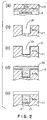
FIGS. 2(a) to 2(e) are a process chart showing an example
of a method for producing the semiconductor device according to the
present invention;
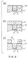
FIGS. 3(a) to 3(c) are a process chart showing an example
of a method for producing the semiconductor device according to the
present invention;
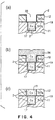
FIGS. 4(a) to 4(c) are a process chart showing an example
of a method for producing the semiconductor device according to the
present invention;
FIG. 5 is a sectional view showing an ECR plasma processing
apparatus for performing a WCN film-forming process;
FIG. 6 is a graph showing the results of X-ray diffraction
of the WCN film;
FIG. 7 is a graph showing the relationship between the flow
rate of C2H4 and the half-width;
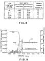
FIG. 8 is a table showing the relationship among the flow
rate of C2H4, the half-width, and the barrier properties against Cu;
FIG. 9 is a graph showing the results of SIMS analysis of
the semiconductor device;
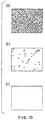
FIGS. 10(a) to 10(c) are schematic views for illustrating
a method for evaluating the barrier properties against Cu;
FIG. 11 is a table showing the relationship among a
hydrocarbon gas, the half-width, and the barrier properties against
Cu;
FIG. 12 is a sectional view for illustrating coverage;
FIG. 13 is a table for comparing coverage by a WCN film and
coverage by a WN film;
FIG. 14 is a table for comparing adhesion of a WCN film and
adhesion of a WN film;
FIG. 15 is a table for showing the relationship between the
proportions of C and N in a WCN film and the adhesion of the WCN
film;
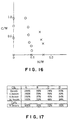
FIG. 16 is a graph for showing the relationship between the
proportions of C and N in a WCN film and the adhesion of the WCN
film;
FIG. 17 is a table showing the relationship between the flow
rate of CF4 and coverage;
FIG. 18 is a graph showing the results of SIMS analysis of
the semiconductor device;
FIG. 19 is a view schematically showing the constitution
of a parallel plate type plasma processing apparatus for a WCN
film-forming process;
FIG. 20 is a graph explaining the relationship between the
process temperature/the process pressure and the resistivity of the
resulting WCN film.
FIG. 21 is a table showing the relationship between the
crystallinity and the resistivity.
DESCRIPTION OF THE PREFERRED EMBODIMENTS
The concrete structure of a semiconductor device according
to the present invention will now be described with reference to
FIG. 1. This drawing shows a part of the semiconductor device. The
reference numerals 11 to 14 in the drawing are each an interlayer
insulator film comprising a SiO2 film and having a thickness of, for
example, about 5,000 angstroms. The reference numerals 15 and 16
are each a wiring layer comprising a Cu layer, for example, about
5,000 angstroms thick. The reference numerals 17 and 18 are each
a connecting layer comprising a Cu layer and connecting the Cu wiring
layers 15 and 16 together.
A barrier film 2 is formed between the Cu wiring layers 15,
16, the Cu connecting layers 17, 18 and the SiO2 films 11 to 14, i.e.,
on the side walls and bottom walls of the Cu wiring layers 15, 16
and the Cu connecting layers 17, 18. The barrier film 2 is a copper
diffusion preventing film comprising a WCN film as a crystalline
film containing W, C and N and having a thickness of, for example,
200 angstroms. In the present embodiment, moreover, an SiN film 19,
for example, about 200 angstroms thick is formed between the SiO2
films adjacent vertically.
An example of a method for producing such a semiconductor
device will be described with reference to FIGS. 2(a) to 2(e) to
4(a) to 4(c). As shown in FIG. 2(a), an SiO2 film 11 is formed on
the surface of a substrate 3. The SiO2 film 11 is formed by converting
film forming gases into a plasma, for example, with the use of an
Ar gas as a plasma gas, and an SiH4 gas and an O2 gas as the film
forming gases, for example, in an ECR plasma processing apparatus
(see FIG. 5) utilizing ECR (electron cyclotron resonance) to be
described later on.
The ECR plasma processing apparatus for performing ECR
plasma treatment will now be described briefly, referring to FIG.
5. The interior of a vacuum vessel 4 comprising a plasma chamber
4A and a film forming chamber 4B is supplied with a high frequency
wave (microwave) M of, for example, 2.45 GHz from a high frequency
power source unit 41 via a wave guide 42 and a transmissive window
43. A magnetic field B, directed from the plasma chamber 4A toward
the film forming chamber 4B and having a magnetic intensity of 875
gausses near an ECR point P, is formed by a main electromagnetic
coil 44a and an auxiliary electromagnetic coil 44b provided around
the plasma chamber 4A and below the film forming chamber 4B,
respectively. By the interaction between the magnetic field B and
the microwave M, electron cyclotron resonance is generated at the
ECR point P.
To form the SiO2 film 11 by this device, a substrate, e.g.,
a semiconductor wafer (hereinafter referred to as "wafer"), 10 is
placed on a table 45 provided in the film forming chamber 4B in the
vacuum vessel 4 which is maintained beforehand in a predetermined
vacuum atmosphere. A plasma gas, e.g. an Ar gas, is introduced into
the plasma chamber 4A via a plasma gas supply pipe 48. The microwave
M of, for example, 2.45 GHz is supplied from the high frequency power
source unit 41 into the vacuum vessel 4. Also, the magnetic field
B is formed by the main electromagnetic coil 44a and the auxiliary
electromagnetic coil 44b. Then, film forming gases are introduced
into the film forming chamber 4B via a film forming gas supply section
49. Then, a bias voltage is applied to the bearing stand 45 by a
high frequency power source unit 46. In this manner, the film forming
gases are converted into a plasma by electron cyclotron resonance
to perform film forming treatment.
Then, treatment for forming a Cu connecting layer 17 in the
SiO2 film 11 is carried out. According to this treatment, as shown
in FIG. 2(b), a via hole 31 is formed for burying Cu in that portion
in the surface of the SiO2 film 11 where a connecting line of Cu is
to be formed. The via hole 31 is formed by forming a predetermined
pattern in the surface of the SiO2 film 11, and etching the pattern
by an etching device (not shown).
Then, as shown in FIG. 2(c), a WCN film 2 is formed on the
entire surface of the SiO2 film 11 where the via hole 31 has been
formed. At this time, an Ar (argon) gas, for example, is used as
a plasma gas, and gases containing tungsten (W), nitrogen (N),
hydrogen (H), and carbon (C), such as WF6 gas, N2 gas, C2H4 gas and
H2 gas, are used as film forming gases. An example of the concrete
process conditions is microwave power 2.7 kW, main electromagnetic
coil current 83A, auxiliary electromagnetic coil current 0A,
introduced gas flow rates WF6/N2/C2H4/H2/Ar = 8.3/8.3/8.3/83.3/100
(unit: sccm), wafer temperature 330°C, and process pressure 0.27 Pa.
Under these process conditions, the film forming gases are converted
into a plasma. Using this plasma, the WCN film 2 is formed on the
entire surface of the SiO2 film 11, including the inner wall surface
of the via hole 31.
The present invention is characterized by using a WCN film,
especially a crystalline WCN film, as the barrier film. Although
the composition of the WCN film is expressed as WCxNy, the WCN film
is described herein as a "WCN" film for simplicity. The composition
of the WCN film can be set in a predetermined range by varying the
flow rate ratio of the respective film forming gases.
Then, as shown in FIG. 2(d), a Cu layer 32 is formed on the
surface of the WCN film 2, etc. to bury Cu in the via hole 31. Then,
as shown in FIG. 2(e), a CMP treatment (polishing treatment) is
performed by a CMP device (not shown) to remove the unnecessary Cu
layer 32 and WCN film 2 on the surface of the SiO2 film 11, i.e.,
the Cu layer 32 and the WCN film 2 other than that on the inner wall
surface of the via hole 31, by polishing. In this manner, Cu is buried
in the via hole 31, formed in the SiO2 film 11, via the WCN film 2
to form a Cu connecting layer 17.
Then, a treatment is performed for forming a Cu wiring layer
15 on the surface of the SiO2 film 11 in which the Cu connecting layer
17 has thus been formed. According to this treatment, as shown in
FIG. 3(a), an SiN film 19 is formed on the surface of the SiO2 film
11. This treatment is performed by converting film forming gases
into a plasma with the use of an Ar gas as a plasma gas, and an SiH4
gas and an N2 gas as the film forming gases, in the aforementioned
ECR plasma processing apparatus.
Then, as shown in FIG. 3(b), an SiO2 film 12 is formed on
the surface of the SiN film 19, for example, by the same method as
in the step shown in FIG. 2(a). At this time, diffusion of Cu from
the Cu connecting layer 17 to the SiO2 film 12 is prevented, because
the SiN film 19 is interposed between the SiO2 film 11 and the SiO2
film 12.
Then, as shown in FIG. 3(c), a trench 33, intended to bury
Cu in the portion of the surface of the SiO2 film 12 where wiring
of Cu is to be formed, is formed by the same method as in the step
shown in FIG. 2(b). Then, as shown in FIG. 4(a), a WCN layer 2 is
formed on the entire surface of the SiO2 film 12, in which the trench
33 has been formed, for example, by the same method as in the step
shown in FIG. 2(c).
Then, as shown in FIG. 4(b), a Cu layer 34 is formed on the
surface of the WCN film 2 to bury Cu in the trench 33. Then, as shown
in FIG. 4(c), a CMP treatment is performed to form a Cu wiring layer
15.
The so produced semiconductor device has a barrier film
comprising the WCN film 2. Thus, as demonstrated by the results of
experiments to be described later on, diffusion of Cu from the Cu
wiring layer 15 or the Cu connecting layer 17 into the SiO2 film 11,
etc., as interlayer insulator films, is prevented. Thus, damage to
the device due to diffusion of Cu into the insulator film is inhibited,
the reliability of the semiconductor device is enhanced, and the
quality of the semiconductor device is improved.
A WCN film was actually formed, and its characteristics were
measured by the X-ray diffraction method. The WCN film was formed
under the following process conditions by means of the ECR plasma
processing apparatus shown in FIG. 5: Microwave power 2.7 kW, main
electromagnetic coil current 83A, auxiliary electromagnetic coil
current 0A, introduced gas flow rates HF6/N2/C2H4/H2/Ar =
8.3/8.3/4.2/83.3/100 (unit: sccm), wafer temperature 330°C, and
process pressure 0.26 Pa. As a result, the WCN film was confirmed
to be crystalline. That is, when the WCN film was subjected to the
X-ray diffraction using an X-ray tube of Cu, a spectrum having peaks
at 36.577 degrees and 42.363 degrees was appeared, as shown in FIG.
6.
The detailed structure of the WCN film is unknown, but
according to the ASTM data, peaks of W2N are known to appear at 37.77
degrees and 43.89 degrees. When C is incorporated into the W2N
structure, the structure may change, and the peak positions may shift,
causing the peaks to appear at positions displaced by several degrees.
Hence, these two peaks are presumed to result from WCN. Thus, the
WCN film is understood to have a crystal structure. When the height
of the peak was designated as h, the half-width that means the width
at a half of the height (i.e. h/2), was 1.554 degrees for the peak
at 36.577 degrees, and 0.841 degree for the peak at 42.363 degrees.
Next, an explanation will be offered for an example of
experiments conducted to ascertain the relationship between the
crystallinity of the WCN film and its copper diffusion preventing
properties (barrier properties). A WCN film was formed under the
following process conditions by means of the ECR plasma processing
apparatus shown in FIG. 5: Microwave power 2.7 kW, main
electromagnetic coil current 83A, auxiliary electromagnetic coil
current 0A, introduced gas flow rates WF6/N2/C2H4/H2/Ar =
8.3/8.3/0-33.3/83.3/100 (unit: sccm), wafer temperature 330°C, and
process pressure 2.5-2.8 Pa. On this occasion, X-ray diffraction
was performed of the WCN films formed under the respective conditions,
with the flow rate of C2H4 being varied in the range of 0 to 33.3
sccm, and the barrier properties of the WCN films against Cu were
measured.
The barrier properties were evaluated by the following
method: A WCN film 500 Angstroms thick was formed on a silicon
substrate under the above-described process conditions. A film of
Cu 5,000 Angstroms thick was formed on the WCN film by sputtering
to prepare a sample. This sample was annealed in an N2 atmosphere
for 30 minutes at a temperature of 600°C, and then subjected to SIMS
(secondary ion mass spectroscopy) to analyze the amounts of Cu, WCN
and Si. The sample was also observed microscopically for the surface
of Cu after annealing.
The results are shown in FIGS. 7, 8 and 9. FIG. 7 shows the
relationship between the flow rate of C2H4 and the half-width for
each of the peak at 36° to 38°, i.e., "the first peak", and the peak
at 42° to 44°, i.e., "the second peak", the peaks ascribed to the
WCN film. FIG. 8 shows the relationship among the flow rate of C2H4,
the crystallinity of the WCN film, and its barrier properties. FIG.
9 shows the results of analysis by SIMS.
In FIG. 8, the crystallinity of the WCN film is expressed
as the half-widths for the two peaks in the X-ray diffraction due
to the WCN film. The barrier properties of the WCN film are evaluated
by the above-mentioned microscopic observation. The barrier
properties were evaluated on a scale of three grades,○,▵, ×. ○
represents that the barrier properties are "excellent", ▵
represents that the barrier properties are "acceptable", and ×
represents that the barrier properties are "poor". FIGS. 10(a) to
10(c) schematically show the occurrence of pits P on the surface
of Cu because of diffusion of Cu into the silicon substrate. When
the pits P occurred in large amounts on the Cu surface as in FIG.
10(a), the barrier properties were evaluated as "poor" (×). When
the pits P occurred in small amounts as in FIG. 10(b), the barrier
properties were evaluated to be "acceptable" (▵). When no pits P
occurred as in FIG. 10(c), the barrier properties were evaluated
as "excellent" (○).
As shown in FIG. 7, as the flow rate of C2H4 increased, the
half-width was confirmed to increase for each of the first peak and
the second peak. It is known that the narrower the half-width, the
better the crystallinity. Thus, it is seen that the smaller the
amount of C2H4 added, the better the crystallinity becomes.
FIG. 8 shows that when the half-width of the first peak is
3.1 or less, the barrier properties are acceptable, and particularly
when it is 2.3 or less, diffusion of Cu can be prevented, and the
barrier properties are excellent. It is also shown that when the
half-width of the second peak is 2.5 or less, the barrier properties
are acceptable, and particularly when it is 1.8 or less, diffusion
of Cu can be prevented, and the barrier properties are excellent.
Since the narrower the half-width, the better the crystallinity,
as stated above, a WCN film with satisfactory crystallinity is found
to have satisfactory barrier properties against Cu.
According to the results of analysis in FIG. 9, the
horizontal axis represents the position in the depth direction of
the sample, while the vertical axis represents the number of Cu ions
etc. in a unit volume. From FIG. 9, it is seen that "Cu is present
in the surface of the WCN film or halfway in the surface, but stops
at a certain depth, and does not exit at a depth corresponding to
the Si substrate." This outcome demonstrates that Cu does not
diffuse into the Si substrate, and the barrier properties of the
WCN film are high.
As discussed above, the crystalline WCN film has
satisfactory barrier properties. The reason may be that the film
is so dense because of the arrangement of crystals as to make passage
of Cu difficult. Moreover, since the film is crystalline, its
structural change due to a temperature rise does not occur, so that
the barrier properties do not change.
In the above-described process, C2H4 is added as a film
forming gas for formation of the WCN film. C2H4 is a hydrocarbon gas
having a double bond. Experiments were conducted to confirm
influences which the addition of such a hydrocarbon gas having a
double bond or a triple bond exerts on the crystallinity and barrier
properties of a WCN film. A WCN film was formed under the following
process conditions by means of the ECR plasma processing apparatus
shown in FIG. 5: Microwave power 2.0 kW, main electromagnetic coil
current 83A, auxiliary electromagnetic coil current 0A, wafer
temperature 330°C, and process pressure 2.5-2.8 Pa. On this occasion,
an Ar gas was used as a plasma gas, a WF6 gas, an N2 gas, and an H2
gas were used as film forming gases other than hydrocarbon, and one
of a C2H6 gas having a single bond, a C2H4 gas having a double bond,
and a C2H2 gas having a triple bond was used as a hydrocarbon gas
to form the WCN film. The flow rates of the introduced gases were
WF6/N2/hydrocarbon gas/H2/Ar = 8.3/8.3/8.3/83.3/100 (unit: sccm).
The so obtained WCN films were each subjected to X-ray diffraction,
and their barrier properties against Cu were confirmed by the
aforementioned method.
The results are shown in FIG. 11. The half-width was found
to increase in the following order for both of the first and second
peaks:
C2H2 gas < C2H4 gas < C2H6 gas
This finding shows that the use of a hydrocarbon gas having a double
bond or a triple bond gives better crystallinity than the use of
a hydrocarbon gas having a single bond, and this use also improves
barrier properties against Cu accordingly.
An investigation of the experimental results shown in FIGS.
8 and 11 combined together shows that the barrier properties against
Cu are acceptable when the half-width of the first peak is 3.2 or
less, and the barrier properties are excellent particularly when
the half-width is 2.3 or less; and that the barrier properties are
acceptable when the half-width of the second peak is 2.6 or less,
and the barrier properties are excellent particularly when the
half-width is 1.8 or less.
The WCN film formed by the above-described method is
satisfactory in the coverage as well as the barrier properties. The
coverage herein refers to an index expressed as B/A and C/A when
the film thickness at a shoulder portion of a concave is designated
as A, the film thickness on the side wall of the concave is designated
as B, and the film thickness at the center of the bottom wall of
the concave is designated as C, as shown in FIG. 12. The greater
the value of this index, the better coverage the film has.
In connection with a WN film and a WCN film hitherto
considered as barrier films, experiments were conducted to compare
their coverages for a concave with an aspect ratio of 5.2 (depth
2.2 µm, width 0.425 µm).
The WCN film was formed by means of the ECR plasma processing
apparatus shown in FIG. 5, and the process conditions were as follows:
Microwave power 2.7 kW, main electromagnetic coil current 83A,
auxiliary electromagnetic coil current 0A, introduced gas flow rates
WF6/N2/C2H4/H2/Ar = 8.3/8.3/8.3/83.3/100 (unit: sccm), wafer
temperature 330°C, and process pressure 0.27 Pa. The WN film was
formed with the use of the same ECR plasma processing apparatus,
and the process conditions were as follows: Microwave power 2.7 kW,
main electromagnetic coil current 83A, auxiliary electromagnetic
coil current 0A, introduced gas flow rates WF6/N2/H2/Ar =
8.3/8.3/83.3/100 (unit: sccm), wafer temperature 330°C, and process
pressure 0.27 Pa.
As a result, the film thickness of the A portion was 2,500
Angstroms for the WCN film, and 1,250 Angstroms for the WN film.
The coverages at the respective sites are shown in FIG. 13. In the
drawing, D denotes the film thickness at a site of the bottom wall
which is near the side wall of the concave. The results show that
the WCN film gives better coverage than the WN film at all sites
of the concave.
The reason for the better coverage may be as follows:
Reactions involving WF6 and N2 are considered to be
WF6 + N2 → WN + NF3
WF6 + N2 + H2 → WN + HF
WF6 + N2 + C2H4 → WCN + HF
The WCN film is formed by the reaction of Formula (3), while the
WN is formed by the reaction of Formula (1) and the reaction of Formula
(2).
The magnitude of the thermal energy of the reaction is
Formula (1) > Formula (2) > Formula (3). The reaction of Formula
(3) is the lowest in thermal energy, and easily occurs as a thermal
reaction. In the above-described process, the WCN film or WN film
is formed by plasma CVD, but the plasma does not hit the side wall
portion (B portion) of the concave, so that the side wall portion
has the film formed by a thermal reaction. For film formation in
the side wall portion, therefore, the reaction of Formula (3) that
is most apt to occur as a thermal reaction is advantageous. Hence,
the WCN film is presumed to cause better coverage. The shoulder
portion (A portion) and the bottom portion (C portion, D portion)
of the concave are bombarded with the plasma, which results in film
formation. If the coverage for the side wall portion (B/A) is
increased, the coverage for the bottom portion (C/A, D/A) also
increases. Thus, the coverage for the side wall portion poses a
problem as stated before.
As noted above, when the coverage for the side wall portion
of the concave becomes satisfactory, the film thickness of the WCN
film in the side wall portion increases. This obtains the effect
of suppressing the lateral diffusion of the Cu wiring layer between
the Cu wiring layer and the SiO2 film in which the Cu wiring layer
has been formed.
Furthermore, the WCN film formed by the above-described
method has good adhesion to the insulator film. Experiments were
conducted to compare the adhesion of a WCN film and a WN film to
an SiO2 film and an SiN film. The reason why the SiO2 film and the
SiN film were selected as the objects for evaluation of adhesion
is that only these films contact the WCN film in the semiconductor
device shown in FIG. 1.
A WCN film and a WN film were formed under the same process
conditions as in the coverage comparison test, and they were measured
for adhesiveness by the stud pull method. The results shown in FIG.
14 were obtained, revealing that the WCN film had higher adhesion
to the SiO2 film and the SiN film. The reason for the satisfactory
adhesion of the WCN film may be that the C of the WCN film is well
bound to SiO2 or the Si of the SiN film, whereby a C-Si bond is formed
between the WCN film and the SiO2 film or the like, and this bond
suppresses peeling between both films. When the adhesion between
the insulator film, such as SiO2 film or SiN film, and the WCN film
in contact therewith is satisfactory, the effect that film
exfoliation between both films is prevented can be obtained.
Then, the following experiments were conducted to confirm
the relationship between the proportions of C and N in a WCN film
and the adhesion of the film: In the experiments, an Ar gas was used
as a plasma gas, and a WF6 gas, a C2H4 gas, an N2 gas, and an H2 gas
were used as film forming gases. A WCN film was formed under the
following process conditions by means of the ECR plasma processing
apparatus shown in FIG. 5: Microwave power 2.7 kW, main
electromagnetic coil current 83A, auxiliary electromagnetic coil
current 0A, wafer temperature 330°C, and process pressure 0.27 Pa.
On this occasion, the flow rate of the WF6 gas was set at 8.3 sccm
(constant), and the flow rate of the H2 gas was set at 83.3 sccm
(constant). The flow rate of the C2H4 gas was varied in the range
of 0 sccm to 41.7 sccm, and the flow rate of the N2 gas was varied
in the range of 0 sccm to 16.7 sccm. As a result, WCN films of
different compositions with the C/W ratio being 0 to 1.23, and the
N/W ratio being 0 to 0.79 were formed. The adhesion of the WCN films,
prepared under the respective conditions, to an SiO2 film and an SiN
film was measured by the stud pull method.
The results are shown in FIGS. 15 and 16. In FIG. 16, the
vertical axis represents the C/W ratio, while the horizontal axis
represents the N/W ratio. (○) signifies that the adhesion to each
of the SiO2 film and the SiN film is 3 kpsi or more, and (×) signifies
the adhesion of less than 3 kpsi.
These results show that the adhesion between the WCN film
and the SiO2 film and the SiN film depends on the proportions of C
and N, and that to obtain adhesion to an SiO2 film and an SiN film
of 3 kpsi or more, it is desirable to set the C/W ratio and the N/W
ratio in the ranges: 0.12<C/W<1.23 and 0<N/W<0.49.
The WCN film formed by the above-described method is lower
in resistance than the WN film. Experiments for confirming this fact
were conducted. A WCN film and a WN film, each 1,000 angstroms thick,
were formed under the same process conditions as for the evaluation
of coverage. Resistivities at 49 points in the plane of each of the
WCN film and the WN film were measured. The average of the
resistivity was 145 µΩcm for the WCN film, and 237 µΩcm for the WN
film.
To form the WCN film of the present invention, a C-F compound
gas (hereinafter referred to as "CF-based gas"), e.g. CF4 gas, may
be used instead of a hydrocarbon gas, as the gas containing C among
the film forming gases. In this case, coverage can be increased
further.
Experiments were performed to compare film coverage of a
concave with an aspect ratio of 5.2 when a WCN film was formed using
a hydrocarbon gas and when a WCN film was formed using a CF-based
gas.
To form a WCN film with the use of a CF-based gas, the ECR
plasma processing apparatus shown in FIG. 5 was used, and the
following process conditions were employed: Microwave power 2.7 kW,
main electromagnetic coil current 83A, auxiliary electromagnetic
coil current 0A, introduced gas flow rates WF6/N2/CF4/H2/Ar =
8.3/8.3/0-16.7/83.3/100 (unit: sccm), wafer temperature 330°C, and
process pressure 2.5-2.7 Pa. On this occasion, the flow rate of the
CF4 gas was varied in the range of 0 sccm to 16.7 sccm. The process
conditions when the hydrocarbon gas was used were the same as in
the previously mentioned coverage evaluation test.
The results are shown in FIG. 17. The results demonstrate
that the formation of the WCN film using the CF-based gas improved
coverage at all sites of the concave. The reason may be that CF4
causes a WCN formation reaction in a vapor phase less frequently,
and a surface reaction more frequently, than C2H4.
The WCN film formed under the foregoing process conditions
with the use of the CF-based gas was subjected to X-ray diffraction.
The aforementioned first and second peaks were confirmed to exist.
This finding made sure that a crystalline WCN film could be formed
even using a CF-based gas. The WCN film was also evaluated for the
barrier properties against Cu, and adhesion to an SiO2 film and an
SiN film. The WCN film was found to have the same barrier properties
and adhesion as when a hydrocarbon gas was used.
According to the present invention, moreover, the barrier
film may be formed from a WC film. The WC film refers to a film
containing W and C, and its film composition is expressed as WCx.
This composition can be set in a predetermined range by changing
the flow rate ratio of the film forming gases to be described later
on.
The WC film is formed by converting film forming gases into
a plasma, for example, with the use of an Ar gas as a plasma gas,
and gases containing W and C, such as a WF6 gas, a C2H4 gas, and an
H2 gas as the film forming gases, for example, in the ECR plasma
processing apparatus shown in FIG. 5. Concretely, the WC film can
be formed under the following process conditions: Microwave power
2.7 kW, main electromagnetic coil current 83A, auxiliary
electromagnetic coil current 0A, introduced gas flow rates
WF6/C2H4/H2/Ar = 8.3/8.3/50/100 (unit: sccm), wafer temperature 330°C,
and process pressure 0.27 Pa.
The WC film was formed under the above process conditions.
To confirm the barrier properties of the WC film against Cu, SIMS
analysis was made. As a result, Cu was found not to diffuse into
an Si substrate, as shown in FIG. 18. Thus, a WC film is understood
to have high barrier properties similarly to a WCN film.
The WC film formed under the above-mentioned process
conditions was measured for adhesion to an SiO2 film and an SiN film
by the stud pull method. The adhesion was 5.8 kpsi for the SiO2 film,
and 6.2 kpsi for the SiN film, showing the WC film to have higher
adhesion to these films than does a WCN film. Film coverage by the
WC film was evaluated, showing that the WC film gives better coverage
than a WN film.
In the semiconductor device according to the present
invention, an SiOF film or a CF film may be used as the interlayer
insulator film, besides an SiO2 film. The CF film has drawn attention
as a film with low specific inductive capacity, but involves the
problem of low adhesion. Thus, the adhesion between the CF film and
a WCN film was evaluated in the following manner:
A CF film 7,000 angstroms thick was formed on the surface
of an SiN film, and a WCN film 1,000 angstroms thick was formed on
the surface of the CF film to prepare a sample. A tape was stuck
to the surface of the WCN film, and whether peeling would occur between
the CF film and the WCN film when the tape was removed was observed
visually. For comparison, the same evaluation was made using a
sample having a WN film formed instead of the WCN film.
No peeling was observed between the CF film and the WCN film,
while peeling was noted between the CF film and the WN film, showing
the WCN film to be higher in adhesion to the CF film than the WN
film. The process conditions for the WCN film and the WN film were
the same as in the aforementioned evaluation of coverage. The same
evaluation was performed for a WCN film and a WC film which were
formed using a CF-based gas. No peeling was observed between each
of these films and a CF film.
As described above, adhesion between a WCN film and a CF
film is satisfactory. Likewise, satisfactory adhesion is obtained
when a WCN film or WC film with a thickness of several tens of Angstroms
is formed on the surface of an interlayer insulator film such as
a CF film, and a WN film is formed on this surface.
According to the present invention, moreover, WCl6 gas,
(C5H5)2WH2 gas, [(CH3)2N]6W2 gas, W[N(CH3)2]6 gas, W[N(C2H5)2]6 gas, and
(C3H7C5H5)2WH2 gas can be used, in addition to WF6 gas, as the gas
containing W among film forming gases for a WCN film. As the
hydrocarbon gas, CH4 gas, C6H6 gas, and (C6H5)CH3 gas can be used in
addition to C2H4 gas, C2H2 gas, and C2H6 gas. As the gas containing
N and H, NH3 gas can be used. As the CF-based gas, C2F6 gas, C4F8 gas,
C5F8 gas, C6F6 gas, C6F10 gas, and C6F5CF3 (perfluorotoluene) gas can
be used in addition to CF4 gas. Further, a CHF-based gas, such as
C2H2F4 gas, CHF3 gas, C2H2F2 gas, C6H4(CF3)2 (1,4-bistrifluoromethylbenzene)
gas, may be used.
According to the film forming process of the present
invention, film forming gases containing W, C, N and H may be used
at an initial stage of film formation to form a film, and then film
forming gases containing W, N and H may be used to form a film. In
this case, a WCN film is formed on the surface of an insulator film,
and a WN film is formed on the upper surface of the WCN film. Since
the WCN film is formed on the surface of the insulator film, coverage
and adhesion to the insulator film are satisfactory, and the barrier
properties against Cu are also satisfactory.
According to the present invention, moreover, the WCN film
is formed by use of ECR as a plasma generative energy. However, for
example, an apparatus that generates plasma by a method called ICP
("inductive couple plasma"), in which an electric field and a
magnetic field are imparted to a process gas from a coil wound round
a dome-shaped vessel, may be used. Also, an apparatus that generates
a plasma by a method called a "helicon wave plasma", in which the
interaction between a helicon wave of, for example, 13.56 MHz and
a magnetic field applied by a magnetic coil, may be used. Furthermore,
an apparatus that generates a plasma by a method called a "magnetron
plasma", in which a magnetic field is applied so as to be almost
parallel to two parallel cathodes, may be used.
Furthermore, an apparatus device called a "parallel plates
type" that generates a plasma by a method, in which a high frequency
power is applied between opposed electrodes, may be used. A test
was conducted to form a WCN film by use of a parallel plates type
plasma processing apparatus as shown in FIG. 19. The parallel plate
type plasma processing apparatus used will be explained briefly.
A table 52 having a heater, an electrostatic chuck, and a lower
electrode (not shown) is provided in a lower portion within a vacuum
vessel 51 of the plasma processing apparatus of parallel plates type.
The lower electrode of the table 52 is supplied with an RF power
by a lower RF power source 53. A shower head 54 having an upper
electrode (not shown) to be supplied with an RF power by an upper
RF power source 55 is provided in an upper portion of the vacuum
vessel 51. The interior of the vacuum vessel 51 can be reduced in
pressure by a vacuum pump (not shown). Various gases can be
introduced into the vacuum vessel 51 from a gas supply source (not
shown) via the shower head 54.
The process conditions for formation of the WCN film were
as follows: An RF power of 1.5 kW given at 60 MHz to the upper
electrode (no RF power given to the lower electrode), introduced
gas flow rates WF6/N2/C2H4/H2/Ar = 8.3/8.3/4.2/83.3/100 (unit: sccm),
wafer temperature 360°C, and process pressure 0.7 Pa. As a result,
it was confirmed that a WCN film having characteristics comparable
to those obtained with the use of an ECR plasma processing apparatus
was obtained.
Finally, a test was conducted to investigate the effects
of the process temperature (wafer temperature) and process pressure
on the crystallinity of a WCN film. The results are described here.
A WCN film was formed using the ECR plasma processing apparatus shown
in FIG. 5. Of the process conditions, the wafer temperature was
varied in the range of 209 to 476°C, the process pressure was varied
in the range of 0.33 to 20 Pa, and the microwave power was varied
in the range of 1 to 4 kW. The other process conditions were the
main electromagnetic coil current 79A, auxiliary electromagnetic
coil current 0A, and constant introduced gas flow rates
WF6/N2/C2H4/H2/Ar = 4.7/2.3/4.7/93/100 (unit: sccm). Data obtained
are shown in FIG. 20 as the relationship between the process
pressure/process temperature and the resistivity.
Further, a WCN film was formed using the ECR plasma
processing apparatus shown in FIG. 5. Of the process conditions,
the wafer temperature was varied in the range of 209 to 476°C, and
the process pressure was varied in the range of 0.33 to 20 Pa. The
other process conditions were the microwave power 2.7 kW, main
electromagnetic coil current 79A, auxiliary electromagnetic coil
current 0A, and constant introduced gas flow rates WF6/N2/C2H4/H2/Ar
= 4.7/2.3/4.7/93/100 (unit: scam). Data obtained are shown in FIG.
21 as the relationship between the resistivity and the first
peak/second peak.
FIG. 21 shows that the lower the resistivity, the smaller
the half-widths of the first and the second peak, namely, the higher
the crystallinity of the film. A comparison is made between FIGS.
21 and 8. FIG. 8 shows that when the half-widths of the first and
second peaks are 3.10 and 2.50, respectively, the barrier properties
are acceptable. FIG. 21, on the other hand, shows that when the
half-widths of the first and second peaks are 3.05 and 2.39,
respectively, the resistivity is 347 µΩcm. These findings show that
when the resistivity is at least 347 µΩcm or less, the barrier
properties are acceptable. In consideration of the difference
between the value 3.10 and the value 3.05, and the difference between
the value 2.50 and the value 2.39, it is concluded that when the
resistivity is at least 350 µΩcm or less, a WCN film having acceptable
barrier properties can be obtained. FIG. 8 also shows that when the
half-widths of the first and second peaks are 2.30 and 1.80,
respectively, the barrier properties are excellent. FIG. 21, on the
other hand, shows that when the half-widths of the first and second
peaks are 2.31 and 1.65, respectively, the resistivity is 275 µΩcm.
These findings show that when the resistivity is at least 275 µΩcm
or less, the barrier properties are excellent.
The graph of FIG. 20 will be discussed on the above premise.
In the graph of FIG. 20, the vertical axis represents the resistivity,
and the horizontal axis represents the process pressure and the
process temperature. FIG. 20 shows that to make the resistivity 350
µΩcm or less, namely, to obtain a WCN film having acceptable barrier
properties, the process pressure should be 10 Pa or less. When the
process pressure is 5.8 Pa, the resistivity is 274.7 µΩcm. Thus,
it is found that the process pressure should be 5 Pa or less in order
to obtain a WCN film having excellent barrier properties. Looking
only at the graph of FIG. 20, it appears that a lower process pressure
is necessary to make the crystallinity of a WCN film higher. In fact,
if the process pressure is too low, the formation of a plasma will
be problematical. Thus, the process pressure should preferably be
0.05 Pa or higher.
Similarly, FIG. 20 shows that to make the resistivity 350
µΩcm or less, namely, to obtain a WCN film having acceptable barrier
properties, the process temperature should be 250°C or higher. To
obtain a WCN film having excellent barrier properties, the process
temperature should preferably be 300°C or higher. From FIG. 20, it
is seen that the higher the process temperature, the better barrier
properties the resulting WCN film has. However, the upper limit of
the process temperature should preferably be 500°C or lower. This
is because changes will occur in the characteristics of other layers
formed before formation of the WCN film, e.g., the Cu wiring layer
below the WCN film, or the lowermost P-doped diffusion layer of the
transistor.