EP1170717A2 - Display device and method for driving the same - Google Patents
Display device and method for driving the same Download PDFInfo
- Publication number
- EP1170717A2 EP1170717A2 EP01305795A EP01305795A EP1170717A2 EP 1170717 A2 EP1170717 A2 EP 1170717A2 EP 01305795 A EP01305795 A EP 01305795A EP 01305795 A EP01305795 A EP 01305795A EP 1170717 A2 EP1170717 A2 EP 1170717A2
- Authority
- EP
- European Patent Office
- Prior art keywords
- block
- screen save
- pixels
- pixel
- display
- Prior art date
- Legal status (The legal status is an assumption and is not a legal conclusion. Google has not performed a legal analysis and makes no representation as to the accuracy of the status listed.)
- Granted
Links
Images




Classifications
-
- G—PHYSICS
- G09—EDUCATION; CRYPTOGRAPHY; DISPLAY; ADVERTISING; SEALS
- G09G—ARRANGEMENTS OR CIRCUITS FOR CONTROL OF INDICATING DEVICES USING STATIC MEANS TO PRESENT VARIABLE INFORMATION
- G09G5/00—Control arrangements or circuits for visual indicators common to cathode-ray tube indicators and other visual indicators
-
- G—PHYSICS
- G09—EDUCATION; CRYPTOGRAPHY; DISPLAY; ADVERTISING; SEALS
- G09G—ARRANGEMENTS OR CIRCUITS FOR CONTROL OF INDICATING DEVICES USING STATIC MEANS TO PRESENT VARIABLE INFORMATION
- G09G3/00—Control arrangements or circuits, of interest only in connection with visual indicators other than cathode-ray tubes
- G09G3/20—Control arrangements or circuits, of interest only in connection with visual indicators other than cathode-ray tubes for presentation of an assembly of a number of characters, e.g. a page, by composing the assembly by combination of individual elements arranged in a matrix no fixed position being assigned to or needed to be assigned to the individual characters or partial characters
- G09G3/22—Control arrangements or circuits, of interest only in connection with visual indicators other than cathode-ray tubes for presentation of an assembly of a number of characters, e.g. a page, by composing the assembly by combination of individual elements arranged in a matrix no fixed position being assigned to or needed to be assigned to the individual characters or partial characters using controlled light sources
-
- G—PHYSICS
- G09—EDUCATION; CRYPTOGRAPHY; DISPLAY; ADVERTISING; SEALS
- G09G—ARRANGEMENTS OR CIRCUITS FOR CONTROL OF INDICATING DEVICES USING STATIC MEANS TO PRESENT VARIABLE INFORMATION
- G09G2320/00—Control of display operating conditions
- G09G2320/04—Maintaining the quality of display appearance
- G09G2320/043—Preventing or counteracting the effects of ageing
-
- G—PHYSICS
- G09—EDUCATION; CRYPTOGRAPHY; DISPLAY; ADVERTISING; SEALS
- G09G—ARRANGEMENTS OR CIRCUITS FOR CONTROL OF INDICATING DEVICES USING STATIC MEANS TO PRESENT VARIABLE INFORMATION
- G09G2320/00—Control of display operating conditions
- G09G2320/10—Special adaptations of display systems for operation with variable images
- G09G2320/103—Detection of image changes, e.g. determination of an index representative of the image change
-
- G—PHYSICS
- G09—EDUCATION; CRYPTOGRAPHY; DISPLAY; ADVERTISING; SEALS
- G09G—ARRANGEMENTS OR CIRCUITS FOR CONTROL OF INDICATING DEVICES USING STATIC MEANS TO PRESENT VARIABLE INFORMATION
- G09G2330/00—Aspects of power supply; Aspects of display protection and defect management
- G09G2330/04—Display protection
Definitions
- the present invention relates to a display device and a method for driving the same, and more particularly, to a display device and a method for driving the same that can uniformly maintain a degradation deviation of a whole display panel in upper, lower, left, and right directions in a self-luminescent display device.
- a display device has a degradation deviation on a display panel by driving the display panel.
- self-luminescent display devices such as a cathode ray tube (CRT), a field emission display (FED), a plasma display panel (PDP), and an electroluminescence (EL), are used as display devices. Since such self-luminescent display devices have a variable screen in view of a graphic screen, certain pixels of a panel are not continuously maintained in turn-on or turn-off state.
- the pixels having different lives deteriorate picture quality of the display device.
- FIG. 1 is a diagram showing a display of a general text type.
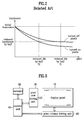
- Luminance according to lives of pixels continuously maintained in turn-off state in FIG. 1 is shown in an upper graph of FIG. 2. As shown in FIG. 2, it is noted that luminance of pixels continuously maintained in turn-on state according to their operation time is remarkably deteriorated as compared with the pixels continuously maintained in turn-off state.
- Luminance of pixels continuously maintained in turn-off state according to their operation time is shown in a lower graph of FIG. 2.
- the pixels continuously maintained in turn-on state charges continuously move within them. Accordingly, as shown in the lower graph of FIG. 2, the pixels continuously maintained in turn-on state have rapidly deteriorated luminance according to life as compared with the pixels continuously maintained in turn-off state. Further, the pixels continuously maintained in turn-on state have a shorter life than the pixels continuously maintained in turn-off state.
- the life difference generates luminance difference between the pixels and deteriorates picture quality of the display device.
- the display device displays a text screen, once the pixels are set up in turn-on or turn-off state, they continuously remain as they are. In this case, luminance difference exists between the turned on pixels and the turned off pixels, thereby remarkably deteriorating picture quality.
- the present invention is directed to a display device and a method for driving the same that addresses problems due to limitations and disadvantages of the related art.
- a display device confirms whether display data applied to a display panel are uniformly maintained for a predetermined time. As a result of confirmation, if the display data are uniformly maintained for a predetermined time, pixels of the display panel are made for a predetermined block unit so that screen save modes are performed to sequentially apply screen save mode data to pixels of each block. The screen save modes are completed after there are sequentially performed for all blocks on the display panel.
- the display device directly displays the display data on the display panel without performing the screen save modes.
- the screen save mode data having a predetermined type to be directly applied to the display panel if the display data are not changed for a predetermined time are in advance stored in a memory of the display device.
- the pixels can be made for one block unit among a block consisting of a plurality of pixel columns, a block consisting of plurality of pixel rows, and N x M (N, M is a positive integer) pixel block.
- screen save mode data designated as turn-on or turn-off are simultaneously applied to all pixels within the same block.
- the pixels are divided into one of the column block, the row block, and the N x M block, and an inverse value of the display data is periodically applied to the pixels within each block.
- certain graphic data can be provided to the display panel at a certain time period to uniformly maintain the degradation state of the whole pixels.
- Pixels of a display device may partially be degraded in view of characteristic of the display device. It is necessary to uniformly compensate display quality of whole pixels so as to uniformly maintain display quality of the partially degraded display device.
- FIG. 3 is a block diagram showing a configuration of a display device according to the present invention.
- the display device of the present invention includes a display panel 10 having a plurality of pixels arranged in a column and row unit, a pixel column driving unit 20 for driving the pixels in column, a pixel row driving unit 30 for driving the pixels in row, and a control unit 40 for driving the pixel column driving unit 20 and the pixel row driving unit 30 using a control signal.
- the control unit 40 divides the pixels into a predetermined block unit by driving the pixel column driving unit 20 and the pixel row driving unit 30 using the control signal.
- the control unit 40 performs screen save modes of the display panel for the predetermined block unit.
- a reference numeral 50 which is not described denotes a memory that stores various types of the screen save modes.
- the predetermined block for the screen save modes may be one of a column block consisting of at least one pixel column, a row block consisting of at least one pixel row, and N x M pixel block consisting of N x M (N, M is positive integer number) pixels.
- the screen save modes may turn on or off all pixels within each block.
- the control unit 40 confirms whether display data applied to the display panel 10 are uniformly maintained for a predetermined time. If the display data are uniformly maintained for a predetermined time, the control unit 40 divides the display panel 10 into at least one block. The screen save modes are then performed. In other words, the display data and the screen save mode data are sequentially applied from the memory 50 to the one block of the display panel 10 under the control of the control unit 40.
- control unit 40 releases the screen save modes and displays the display data only on the display panel 10.
- control unit 40 continuously displays the display data on the display panel 10 without performing the screen save modes.
- Inverse data of the display data may be used as the screen save mode data.
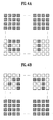
- FIGs. 4A and 4B are diagrams showing screen save modes that turn on pixels of a display device for a column block unit.
- FIGs. 4A and 4B a plurality of columns are regarded as one block unit and pixels are turned on for a block unit, so that the screen save modes are performed.
- FIG. 4A show a first column block of the screen save modes implemented for the column block unit
- FIG. 4B shows the last column block of the screen save modes implemented for the column block unit.
- the control unit 40 confirms whether the display data applied to the display panel 10 are uniformly maintained for a predetermined time. If the display data are uniformly maintained for a predetermined time, the control unit 40 divides the pixels of the display panel 10 into at least one pixel column block. Then, the screen save modes are sequentially performed on the pixel column block.
- the screen save modes mean that pixels corresponding to each pixel column block are simultaneously driven in the same type.
- the same type may be made in such a manner that all pixels within each block are turned on or off.
- control unit 40 releases the screen save modes and displays the display data only on the display panel 10.
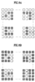
- FIGs. 5A and 5B are diagrams showing screen save modes that turn on pixels for a row block unit.
- FIGs. 5A and 5B a plurality of rows are regarded as one block unit and pixels are turned on for a block unit, so that the screen save modes are performed.
- FIG. 5A show a first row block of the screen save modes implemented for the row block unit
- FIG. 5B shows the last row block of the screen save modes implemented for the row block unit.
- the control unit 40 confirms whether the display data applied to the display panel 10 are uniformly maintained for a predetermined time. If the display data are uniformly maintained for a predetermined time, the control unit 40 divides the pixels of the display panel 10 into at least one pixel row block. Then, the screen save modes are sequentially performed on the pixel row block by the control unit 40.
- the screen save modes mean that pixels corresponding to each pixel row block are simultaneously driven in the same type.
- control unit 40 releases the screen save modes and displays the display data only on the display panel 10.
- the screen save modes for the row block unit are useful for display devices that perform display for a character unit.
- a user can manipulate the display device for the screen save mode for the row block unit without reducing viewing sensitivity when viewing a screen displayed in the display device.
- FIGs. 6A and 6B are diagrams showing screen save modes that turn on pixels for N1 x M1 block unit.
- FIG. 6A show a first N1 x M1 pixel block of the screen save modes implemented for a certain pixel block unit
- FIG. 6B shows the last N1 x M1 pixel block of the screen save modes implemented for the certain pixel block unit.
- Pixels of one N1 x M1 pixel block are turned on while pixels of the other N x M pixel blocks are turned off. These steps are repeated until the screen save modes of all N1 x -M1 pixel blocks are completed.
- the control unit 40 confirms whether the display data applied to the display panel 10 are uniformly maintained for a predetermined time. If the display data are uniformly maintained for a predetermined time, the control unit 40 divides the pixels of the display panel 10 into at least one N1 x M1 (N1 and M1 are positive integers) pixel row block. The screen save mode is then performed on the N1 x M1 pixel block.
- the screen save modes mean that pixels corresponding to each N1 x M1 pixel block are simultaneously driven in the same type.
- control unit 40 releases the screen save mode and displays the display data only on the display panel 10.
- the same type may be made in such a manner that all pixels within each block are turned on or off.
- FIG. 7 is a graph showing lives of pixels according to the present invention.
- a graph at an upper portion shows lives of the pixels of the display device when the screen save modes are performed on the display device for the pixel block unit while a graph at a lower portion shows lives of pixels when the pixels of the display device are continuously turned on without performing the screen save modes.
- FIG. 8A is a diagram showing a screen when the display device is in a general display state while FIG. 8B is a diagram showing a screen when turned on pixels and turned off pixels are inversed on the screen.
- the control unit 40 confirms whether the display data applied to the display panel 10 are uniformly maintained for a predetermined time. If the display data are uniformly maintained for a predetermined time, the control unit 40 divides the pixels of the display panel 10 into at least one pixel block. Then, the control unit 40 sequentially applies the screen save mode data to the pixel block.
- the screen save mode data are inverse data of data corresponding to each pixel block of the display data.
- the block for the screen save modes may be one of a column block consisting of at least one pixel column, a row block consisting of at least one pixel row, and a pixel block consisting of N x M(N1 and M1 are positive integers) pixels.
- the screen save mode data are to turn off the pixels turned on according to the display data among the pixels belonging to each pixel block and at the same time to turn on the pixels turned off according to the display data among the pixels belonging to each pixel block.
- the display panel of the display device has improved picture quality.
- FIG. 9 is a flow chart showing steps of compensating degradation deviation of the display device according to the present invention.
- the control unit 40 of the display device confirms whether the display data are uniformly maintained for a predetermined time (T sec.) without any change (S2). If the display data are continuously changed, the display device continuously performs the display step under the control of the control unit 40. Meanwhile, if it is determined that the display data are continuously displayed on the screen for a predetermined time, the display device is subject to the screen save modes according to the present invention under the control of the control unit 40.
- the screen save modes may be implemented in various types. These various types are previously divided and then stored in the memory of the display device. Also, the types of the screen save modes are previously designated by a user or manufacturer. The display device performs the screen save modes of the previously designated types as above. As an example, the first screen save mode is implemented for a column block unit, the second screen save mode is implemented for a row block unit, and the third screen save mode is implemented for a pixel block unit (S4).
- a driving method of a display device has the following advantages.
- luminance deviation can uniformly be maintained at a small range between the pixels over the whole screen of the display panel. As a result, it is possible to improve picture quality of the screen.
Landscapes
- Engineering & Computer Science (AREA)
- Physics & Mathematics (AREA)
- Computer Hardware Design (AREA)
- General Physics & Mathematics (AREA)
- Theoretical Computer Science (AREA)
- Control Of Indicators Other Than Cathode Ray Tubes (AREA)
- Control Of El Displays (AREA)
Abstract
Description
Claims (23)
- A method for driving a display device having a display panel, the method comprising the steps of:confirming whether display data applied to the display panel are uniformly maintained for a predetermined time;dividing the display panel into at least one block when the display data are uniformly maintained for a predetermined time; andsequentially performing screen save modes that apply the display data and screen save mode data to the one block.
- The method of claim 1, further comprising the steps of:releasing the screen save modes when the display data are changed during the screen save modes; anddisplaying the display data only on the display panel.
- The method of claim 1, further comprising the step of displaying the display data on the display panel without performing the screen save modes when the display data are changed without being uniformly maintained for a predetermined time.
- The method of claim 1, wherein the block for the screen save modes is any one of a column block consisting of at least one pixel column, a row block consisting of at least one pixel row, and a pixel block consisting of N1 x M1 (N1 and M1 are positive integers) pixels.
- The method of claim 1, wherein the screen save mode data are inverse data of the display data.
- The method of claim 1, wherein the screen save mode data are to turn on or off whole pixels within each pixel block.
- A method for driving a display device having a display panel, the method comprising the steps of:confirming whether display data applied to the display panel are uniformly maintained for a predetermined time;dividing the display panel into at least one pixel column block when the display data are uniformly maintained for a predetermined time; andsequentially performing screen save modes on the one pixel column block, the screen save modes simultaneously driving pixels belonging to each pixel column block in one type.
- The method of claim 7, wherein the one type when performing the screen save modes is to turn on or off all pixels within each block.
- The method of claim 7, further comprising the steps of:releasing the screen save modes when the display data are changed during the screen save modes; anddisplaying the display data only on the display panel.
- A method for driving a display device having a display panel, the method comprising the steps of:confirming whether display data applied to the display panel are uniformly maintained for a predetermined time;dividing the display panel into at least one pixel row block when the display data are uniformly maintained for a predetermined time; andsequentially performing screen save modes on the one pixel row block, the screen save modes simultaneously driving pixels belonging to each pixel row block in one type.
- The method of claim 10, further comprising the steps of:releasing the screen save modes when the display data are changed during the screen save modes; anddisplaying the display data only on the display panel.
- The method of claim 10, wherein the one type when performing the screen save modes is to turn on or off all pixels within each block.
- A method for driving a display device having a display panel, the method comprising the steps of:confirming whether display data applied to the display panel are uniformly maintained for a predetermined time;dividing the display panel into at least one N1 x M1 (N1 and M1 are positive integers) pixel block when the display data are uniformly maintained for a predetermined time; andsequentially performing screen save modes on the one N1 x M1 pixel block, the screen save modes simultaneously driving pixels belonging to each N1 x M1 pixel block in one type.
- The method of claim 13, further comprising the steps of:releasing the screen save modes when the display data are changed during the screen save modes; anddisplaying the display data only on the display panel.
- The method of claim 13, wherein the one type when performing the screen save modes is to turn on or off all pixels within each block.
- The method of claim 13, wherein the N1 x M1 pixel block has a size of 11 x 12 pixels or 6 x 12 pixels.
- A method for driving a display device having a display panel, the method comprising the steps of:confirming whether display data applied to the display panel are uniformly maintained for a predetermined time;dividing the display panel into at least one pixel block when the display data are uniformly maintained for a predetermined time; andsequentially applying screen save mode data to the one pixel block, the screen save mode data being inverse data of data belonging to each pixel block of the display data.
- The method of claim 17, wherein the block for the screen save modes is any one of a column block consisting of at least one pixel column, a row block consisting of at least one pixel row, and a pixel block consisting of N x M (N, M is a positive integer) pixels.
- The method of claim 17, wherein the screen save mode data are to turn off pixels turned on according to the display data among pixels belonging to each pixel block and at the same time to turn on pixels turned off according to the display data among the pixels belonging to each pixel block.
- A display device comprising:a display panel having a plurality of pixels arranged in a column unit;a pixel column driving unit for driving the pixel columns;a pixel row driving unit for driving the pixel rows; anda control unit for driving the pixel column driving unit and the pixel row driving unit using a control signal to divide the pixels into a predetermined block unit and performing screen save modes of the display panel for the predetermined block unit.
- The display device of claim 20, further comprising a memory for storing various types of the screen save modes.
- The display device of claim 20, wherein the block for the screen save modes is any one of a column block consisting of at least one pixel column, a row block consisting of at least one pixel row, and a pixel block consisting of N1 x M1 (N1 and M1 are positive integers) pixels.
- The display device of claim 20, wherein the screen save modes are to turn on or off all pixels within each block.
Applications Claiming Priority (2)
| Application Number | Priority Date | Filing Date | Title |
|---|---|---|---|
| KR1020000038010A KR100335092B1 (en) | 2000-07-04 | 2000-07-04 | Drive Control Method for Display Device |
| KR2000038010 | 2000-07-04 |
Publications (3)
| Publication Number | Publication Date |
|---|---|
| EP1170717A2 true EP1170717A2 (en) | 2002-01-09 |
| EP1170717A3 EP1170717A3 (en) | 2002-09-04 |
| EP1170717B1 EP1170717B1 (en) | 2007-05-30 |
Family
ID=19676127
Family Applications (1)
| Application Number | Title | Priority Date | Filing Date |
|---|---|---|---|
| EP01305795A Expired - Lifetime EP1170717B1 (en) | 2000-07-04 | 2001-07-04 | Display device and method for driving the same |
Country Status (5)
| Country | Link |
|---|---|
| US (2) | US7162702B2 (en) |
| EP (1) | EP1170717B1 (en) |
| KR (1) | KR100335092B1 (en) |
| CN (1) | CN1256660C (en) |
| DE (1) | DE60128623T2 (en) |
Cited By (1)
| Publication number | Priority date | Publication date | Assignee | Title |
|---|---|---|---|---|
| EP1677284A3 (en) * | 2004-12-29 | 2009-04-15 | LG Display Co., Ltd. | Light emitting device and method of driving the same |
Families Citing this family (21)
| Publication number | Priority date | Publication date | Assignee | Title |
|---|---|---|---|---|
| KR100335092B1 (en) * | 2000-07-04 | 2002-05-04 | 구자홍 | Drive Control Method for Display Device |
| KR100459407B1 (en) * | 2002-04-30 | 2004-12-03 | 엘지전자 주식회사 | Driving method for field emission display |
| JP3793152B2 (en) * | 2002-12-26 | 2006-07-05 | 株式会社東芝 | Information recording method, information reproducing method, information reproducing apparatus, and information recording medium |
| CN1333317C (en) * | 2003-02-13 | 2007-08-22 | 神达电脑股份有限公司 | security device |
| KR100506609B1 (en) | 2003-08-11 | 2005-08-08 | 삼성전자주식회사 | Display apparatus and control method thereof |
| US7315989B2 (en) * | 2004-12-07 | 2008-01-01 | International Business Machines Corporation | Method, computer program product, and system for a statistical analysis screensaver |
| CN101471059B (en) * | 2007-12-29 | 2011-06-29 | 鸿富锦精密工业(深圳)有限公司 | Screen saver control method and device |
| CN101751847A (en) * | 2008-12-09 | 2010-06-23 | 康佳集团股份有限公司 | Energy saving method and device for plasma television |
| US8230372B2 (en) * | 2009-12-03 | 2012-07-24 | International Business Machines Corporation | Retargeting for electrical yield enhancement |
| DE102010033286B4 (en) * | 2010-08-04 | 2020-12-03 | Kostal Automobil Elektrik Gmbh & Co. Kg | Process for the degradation compensation of an OLED display |
| USD715834S1 (en) * | 2011-11-23 | 2014-10-21 | Opp Limited | Portion of a display screen with color icon or personality assessment interface |
| USD690311S1 (en) * | 2012-01-05 | 2013-09-24 | Nooka Inc. | Display screen with graphical user interface for time keeping |
| KR102014779B1 (en) * | 2012-12-18 | 2019-08-27 | 엘지전자 주식회사 | Electronic apparatus and method of driving a display |
| USD759072S1 (en) * | 2013-06-17 | 2016-06-14 | Opp Limited | Display screen with a personal assessment interface having a color icon |
| KR20150078857A (en) | 2013-12-31 | 2015-07-08 | 엘지디스플레이 주식회사 | Protecting Curcuit of Memory and LCD having the Same |
| KR102228626B1 (en) * | 2014-08-20 | 2021-03-17 | 엘지디스플레이 주식회사 | Display device and timing controller |
| USD863337S1 (en) * | 2018-06-03 | 2019-10-15 | Apple Inc. | Electronic device with animated graphical user interface |
| KR20210105477A (en) * | 2020-02-18 | 2021-08-27 | 삼성디스플레이 주식회사 | Display device and displaying method thereof |
| KR102817740B1 (en) | 2020-10-20 | 2025-06-10 | 삼성디스플레이 주식회사 | Screen saver controller, display device including the same and method of operating a display device including the same |
| WO2022093174A1 (en) * | 2020-10-26 | 2022-05-05 | Hewlett-Packard Development Company, L.P. | Turn on and off screen pixel sets |
| USD1095577S1 (en) * | 2022-12-21 | 2025-09-30 | Nsk Ltd. | Display screen or portion thereof with graphical user interface |
Family Cites Families (18)
| Publication number | Priority date | Publication date | Assignee | Title |
|---|---|---|---|---|
| JPH06332418A (en) | 1993-05-20 | 1994-12-02 | Fujitsu General Ltd | Light emitting surface protection circuit for display device |
| JP3413818B2 (en) * | 1993-12-14 | 2003-06-09 | ソニー株式会社 | Broadcast receiving apparatus and broadcast signal transmitting / receiving method |
| JPH08292740A (en) | 1995-04-20 | 1996-11-05 | Fujitsu General Ltd | Display seizure prevention device |
| US5740549A (en) * | 1995-06-12 | 1998-04-14 | Pointcast, Inc. | Information and advertising distribution system and method |
| JP3520630B2 (en) | 1995-10-20 | 2004-04-19 | 株式会社富士通ゼネラル | Display protection circuit |
| US6084583A (en) * | 1997-12-31 | 2000-07-04 | At&T Corp | Advertising screen saver |
| US6401209B1 (en) * | 1998-03-09 | 2002-06-04 | Micron Technology, Inc. | Method for automatically initiating a computer security and/or screen saver mode |
| WO1999053472A1 (en) | 1998-04-15 | 1999-10-21 | Cambridge Display Technology Ltd. | Display control device with modes for reduced power consumption |
| JP2000010522A (en) | 1998-06-19 | 2000-01-14 | Pioneer Electron Corp | Method and device for controlling luminance of plasma display panel |
| US6313878B1 (en) * | 1998-11-20 | 2001-11-06 | Sony Corporation | Method and structure for providing an automatic hardware-implemented screen-saver function to a display product |
| US6353449B1 (en) * | 1998-12-10 | 2002-03-05 | International Business Machines Corporation | Communicating screen saver |
| US6384852B1 (en) * | 1999-06-09 | 2002-05-07 | International Business Machines Corporation | Intelligent screen saver using image difference |
| JP3279545B2 (en) | 1999-07-01 | 2002-04-30 | 日本電気株式会社 | Display device with burn-in prevention function and burn-in prevention method |
| US7231083B1 (en) * | 1999-10-29 | 2007-06-12 | Intel Corporation | Controlling processor-based systems using a digital camera |
| US6507350B1 (en) * | 1999-12-29 | 2003-01-14 | Intel Corporation | Flat-panel display drive using sub-sampled YCBCR color signals |
| US6522347B1 (en) * | 2000-01-18 | 2003-02-18 | Seiko Epson Corporation | Display apparatus, portable information processing apparatus, information recording medium, and electronic apparatus |
| US6486900B1 (en) * | 2000-06-28 | 2002-11-26 | Koninklijke Philips Electronics N.V. | System and method for a video display screen saver |
| KR100335092B1 (en) * | 2000-07-04 | 2002-05-04 | 구자홍 | Drive Control Method for Display Device |
-
2000
- 2000-07-04 KR KR1020000038010A patent/KR100335092B1/en not_active Expired - Lifetime
-
2001
- 2001-07-03 US US09/897,611 patent/US7162702B2/en not_active Expired - Lifetime
- 2001-07-04 CN CNB011200154A patent/CN1256660C/en not_active Expired - Lifetime
- 2001-07-04 DE DE60128623T patent/DE60128623T2/en not_active Expired - Lifetime
- 2001-07-04 EP EP01305795A patent/EP1170717B1/en not_active Expired - Lifetime
-
2006
- 2006-12-05 US US11/633,497 patent/US7865846B2/en not_active Expired - Fee Related
Cited By (1)
| Publication number | Priority date | Publication date | Assignee | Title |
|---|---|---|---|---|
| EP1677284A3 (en) * | 2004-12-29 | 2009-04-15 | LG Display Co., Ltd. | Light emitting device and method of driving the same |
Also Published As
| Publication number | Publication date |
|---|---|
| CN1331443A (en) | 2002-01-16 |
| US7865846B2 (en) | 2011-01-04 |
| US7162702B2 (en) | 2007-01-09 |
| US20070075991A1 (en) | 2007-04-05 |
| DE60128623T2 (en) | 2008-01-31 |
| US20020003536A1 (en) | 2002-01-10 |
| EP1170717B1 (en) | 2007-05-30 |
| KR100335092B1 (en) | 2002-05-04 |
| CN1256660C (en) | 2006-05-17 |
| KR20020004273A (en) | 2002-01-16 |
| EP1170717A3 (en) | 2002-09-04 |
| DE60128623D1 (en) | 2007-07-12 |
Similar Documents
| Publication | Publication Date | Title |
|---|---|---|
| US7162702B2 (en) | Display device and method for driving the same | |
| US7227521B2 (en) | Image display apparatus | |
| EP0492585B1 (en) | Flat display | |
| US7161574B2 (en) | Liquid crystal display element driving method and liquid crystal display using the same | |
| US7098900B2 (en) | Method of driving display elements and electronic apparatus using the driving method | |
| JP2000020019A (en) | Field emission display | |
| US7142199B2 (en) | Matrix type-flat-panel display device having multi data lines and method for driving the same | |
| JP4995370B2 (en) | Display device | |
| KR20000003327A (en) | Variable voltage apparatus of control white valance for pdp | |
| US20080252567A1 (en) | Active Matrix Display Device | |
| KR100251148B1 (en) | Method for driving three electrodes surface discharge plasma display panel | |
| JP2007121674A (en) | Display device | |
| KR20060104222A (en) | Driving device of electron emission display device and driving method thereof | |
| KR100588755B1 (en) | Data processing circuit and method for driving an active matrix organic light emitting diode panel by time division control method | |
| KR20120028011A (en) | Organic light emitting display and driving method thereof | |
| KR20000003388A (en) | Plasma display paneal, driving apparatus and method thereof | |
| KR100462317B1 (en) | AC PD Drive | |
| KR100352978B1 (en) | Plasma Display Panel and Driving Method Thereof | |
| US8477084B2 (en) | Organic electroluminescence display and method of driving the same | |
| KR100251150B1 (en) | Driving Method of Plasma Display Panel | |
| KR101547215B1 (en) | Organic electroluminescence display device and driving method thereof | |
| JP2006091787A (en) | Flat display device and brightness control method for display device | |
| JP2006071785A (en) | Flat display device and brightness control method for display device | |
| JP2006078590A (en) | Flat display device and drive control method for display device | |
| JP2007041221A (en) | Plasma television |
Legal Events
| Date | Code | Title | Description |
|---|---|---|---|
| PUAI | Public reference made under article 153(3) epc to a published international application that has entered the european phase |
Free format text: ORIGINAL CODE: 0009012 |
|
| AK | Designated contracting states |
Kind code of ref document: A2 Designated state(s): AT BE CH CY DE DK ES FI FR GB GR IE IT LI LU MC NL PT SE TR |
|
| AX | Request for extension of the european patent |
Free format text: AL;LT;LV;MK;RO;SI |
|
| PUAL | Search report despatched |
Free format text: ORIGINAL CODE: 0009013 |
|
| AK | Designated contracting states |
Kind code of ref document: A3 Designated state(s): AT BE CH CY DE DK ES FI FR GB GR IE IT LI LU MC NL PT SE TR |
|
| AX | Request for extension of the european patent |
Free format text: AL;LT;LV;MK;RO;SI |
|
| RIC1 | Information provided on ipc code assigned before grant |
Free format text: 7G 09G 3/20 A, 7G 09G 3/36 B, 7G 09G 5/10 B, 7G 09G 3/28 B |
|
| 17P | Request for examination filed |
Effective date: 20030221 |
|
| 17Q | First examination report despatched |
Effective date: 20030328 |
|
| AKX | Designation fees paid |
Designated state(s): DE FR GB NL |
|
| GRAP | Despatch of communication of intention to grant a patent |
Free format text: ORIGINAL CODE: EPIDOSNIGR1 |
|
| GRAS | Grant fee paid |
Free format text: ORIGINAL CODE: EPIDOSNIGR3 |
|
| GRAA | (expected) grant |
Free format text: ORIGINAL CODE: 0009210 |
|
| AK | Designated contracting states |
Kind code of ref document: B1 Designated state(s): DE FR GB NL |
|
| REG | Reference to a national code |
Ref country code: GB Ref legal event code: FG4D |
|
| REF | Corresponds to: |
Ref document number: 60128623 Country of ref document: DE Date of ref document: 20070712 Kind code of ref document: P |
|
| ET | Fr: translation filed | ||
| PLBE | No opposition filed within time limit |
Free format text: ORIGINAL CODE: 0009261 |
|
| STAA | Information on the status of an ep patent application or granted ep patent |
Free format text: STATUS: NO OPPOSITION FILED WITHIN TIME LIMIT |
|
| 26N | No opposition filed |
Effective date: 20080303 |
|
| REG | Reference to a national code |
Ref country code: NL Ref legal event code: SD Effective date: 20130625 |
|
| PGFP | Annual fee paid to national office [announced via postgrant information from national office to epo] |
Ref country code: NL Payment date: 20150612 Year of fee payment: 15 |
|
| REG | Reference to a national code |
Ref country code: FR Ref legal event code: PLFP Year of fee payment: 16 |
|
| REG | Reference to a national code |
Ref country code: NL Ref legal event code: MM Effective date: 20160801 |
|
| PG25 | Lapsed in a contracting state [announced via postgrant information from national office to epo] |
Ref country code: NL Free format text: LAPSE BECAUSE OF NON-PAYMENT OF DUE FEES Effective date: 20160801 |
|
| REG | Reference to a national code |
Ref country code: FR Ref legal event code: PLFP Year of fee payment: 17 |
|
| REG | Reference to a national code |
Ref country code: FR Ref legal event code: PLFP Year of fee payment: 18 |
|
| PGFP | Annual fee paid to national office [announced via postgrant information from national office to epo] |
Ref country code: FR Payment date: 20190605 Year of fee payment: 19 |
|
| PGFP | Annual fee paid to national office [announced via postgrant information from national office to epo] |
Ref country code: GB Payment date: 20190605 Year of fee payment: 19 Ref country code: DE Payment date: 20190604 Year of fee payment: 19 |
|
| REG | Reference to a national code |
Ref country code: DE Ref legal event code: R119 Ref document number: 60128623 Country of ref document: DE |
|
| GBPC | Gb: european patent ceased through non-payment of renewal fee |
Effective date: 20200704 |
|
| PG25 | Lapsed in a contracting state [announced via postgrant information from national office to epo] |
Ref country code: GB Free format text: LAPSE BECAUSE OF NON-PAYMENT OF DUE FEES Effective date: 20200704 Ref country code: FR Free format text: LAPSE BECAUSE OF NON-PAYMENT OF DUE FEES Effective date: 20200731 |
|
| PG25 | Lapsed in a contracting state [announced via postgrant information from national office to epo] |
Ref country code: DE Free format text: LAPSE BECAUSE OF NON-PAYMENT OF DUE FEES Effective date: 20210202 |