EP1170640A2 - Image forming apparatus - Google Patents
Image forming apparatus Download PDFInfo
- Publication number
- EP1170640A2 EP1170640A2 EP01116313A EP01116313A EP1170640A2 EP 1170640 A2 EP1170640 A2 EP 1170640A2 EP 01116313 A EP01116313 A EP 01116313A EP 01116313 A EP01116313 A EP 01116313A EP 1170640 A2 EP1170640 A2 EP 1170640A2
- Authority
- EP
- European Patent Office
- Prior art keywords
- electrifying
- forming apparatus
- image forming
- image
- conductive
- Prior art date
- Legal status (The legal status is an assumption and is not a legal conclusion. Google has not performed a legal analysis and makes no representation as to the accuracy of the status listed.)
- Withdrawn
Links
- 239000002245 particle Substances 0.000 claims description 84
- 239000010410 layer Substances 0.000 claims description 34
- 229910052751 metal Inorganic materials 0.000 claims description 18
- 239000002184 metal Substances 0.000 claims description 18
- 230000000694 effects Effects 0.000 claims description 6
- 239000002344 surface layer Substances 0.000 claims description 6
- 230000001737 promoting effect Effects 0.000 description 30
- 239000004411 aluminium Substances 0.000 description 13
- 229910052782 aluminium Inorganic materials 0.000 description 13
- XAGFODPZIPBFFR-UHFFFAOYSA-N aluminium Chemical compound [Al] XAGFODPZIPBFFR-UHFFFAOYSA-N 0.000 description 13
- 239000000463 material Substances 0.000 description 13
- 238000000034 method Methods 0.000 description 12
- 230000005684 electric field Effects 0.000 description 11
- 238000012546 transfer Methods 0.000 description 10
- 230000015572 biosynthetic process Effects 0.000 description 8
- 238000010276 construction Methods 0.000 description 8
- 230000001105 regulatory effect Effects 0.000 description 8
- 238000009826 distribution Methods 0.000 description 7
- 239000000843 powder Substances 0.000 description 6
- 230000002093 peripheral effect Effects 0.000 description 5
- XLOMVQKBTHCTTD-UHFFFAOYSA-N Zinc monoxide Chemical compound [Zn]=O XLOMVQKBTHCTTD-UHFFFAOYSA-N 0.000 description 4
- 238000004140 cleaning Methods 0.000 description 4
- 238000007599 discharging Methods 0.000 description 4
- 239000006260 foam Substances 0.000 description 4
- 229910044991 metal oxide Inorganic materials 0.000 description 4
- 150000004706 metal oxides Chemical class 0.000 description 4
- 239000006229 carbon black Substances 0.000 description 3
- 229920001971 elastomer Polymers 0.000 description 3
- 239000000126 substance Substances 0.000 description 3
- JOYRKODLDBILNP-UHFFFAOYSA-N Ethyl urethane Chemical compound CCOC(N)=O JOYRKODLDBILNP-UHFFFAOYSA-N 0.000 description 2
- CBENFWSGALASAD-UHFFFAOYSA-N Ozone Chemical compound [O-][O+]=O CBENFWSGALASAD-UHFFFAOYSA-N 0.000 description 2
- 239000003795 chemical substances by application Substances 0.000 description 2
- 239000011248 coating agent Substances 0.000 description 2
- 238000000576 coating method Methods 0.000 description 2
- 230000007613 environmental effect Effects 0.000 description 2
- 238000005286 illumination Methods 0.000 description 2
- 238000002347 injection Methods 0.000 description 2
- 239000007924 injection Substances 0.000 description 2
- 238000005259 measurement Methods 0.000 description 2
- 229920002379 silicone rubber Polymers 0.000 description 2
- 239000004945 silicone rubber Substances 0.000 description 2
- 229910001220 stainless steel Inorganic materials 0.000 description 2
- 239000010935 stainless steel Substances 0.000 description 2
- 239000000758 substrate Substances 0.000 description 2
- 238000012360 testing method Methods 0.000 description 2
- XOLBLPGZBRYERU-UHFFFAOYSA-N tin dioxide Chemical compound O=[Sn]=O XOLBLPGZBRYERU-UHFFFAOYSA-N 0.000 description 2
- 239000011787 zinc oxide Substances 0.000 description 2
- 239000004925 Acrylic resin Substances 0.000 description 1
- 229920000178 Acrylic resin Polymers 0.000 description 1
- 229920002943 EPDM rubber Polymers 0.000 description 1
- 239000004809 Teflon Substances 0.000 description 1
- 229920006362 Teflon® Polymers 0.000 description 1
- 238000004220 aggregation Methods 0.000 description 1
- 230000002776 aggregation Effects 0.000 description 1
- 238000013019 agitation Methods 0.000 description 1
- PNEYBMLMFCGWSK-UHFFFAOYSA-N aluminium oxide Inorganic materials [O-2].[O-2].[O-2].[Al+3].[Al+3] PNEYBMLMFCGWSK-UHFFFAOYSA-N 0.000 description 1
- 229910021417 amorphous silicon Inorganic materials 0.000 description 1
- 230000005540 biological transmission Effects 0.000 description 1
- 230000000052 comparative effect Effects 0.000 description 1
- 238000013329 compounding Methods 0.000 description 1
- 230000006866 deterioration Effects 0.000 description 1
- 238000011161 development Methods 0.000 description 1
- 238000000445 field-emission scanning electron microscopy Methods 0.000 description 1
- 239000010419 fine particle Substances 0.000 description 1
- 239000006261 foam material Substances 0.000 description 1
- 238000005187 foaming Methods 0.000 description 1
- 239000004088 foaming agent Substances 0.000 description 1
- 238000010438 heat treatment Methods 0.000 description 1
- 239000010954 inorganic particle Substances 0.000 description 1
- 150000002500 ions Chemical class 0.000 description 1
- 239000000314 lubricant Substances 0.000 description 1
- 238000002156 mixing Methods 0.000 description 1
- 239000000203 mixture Substances 0.000 description 1
- 238000000465 moulding Methods 0.000 description 1
- 238000010606 normalization Methods 0.000 description 1
- 230000003287 optical effect Effects 0.000 description 1
- 238000000016 photochemical curing Methods 0.000 description 1
- 238000005498 polishing Methods 0.000 description 1
- 229920006122 polyamide resin Polymers 0.000 description 1
- 238000006116 polymerization reaction Methods 0.000 description 1
- 238000003825 pressing Methods 0.000 description 1
- 230000002265 prevention Effects 0.000 description 1
- 239000011347 resin Substances 0.000 description 1
- 229920005989 resin Polymers 0.000 description 1
- 238000005070 sampling Methods 0.000 description 1
- 238000007790 scraping Methods 0.000 description 1
- 239000002356 single layer Substances 0.000 description 1
- 230000003746 surface roughness Effects 0.000 description 1
- 238000004073 vulcanization Methods 0.000 description 1
- 239000002699 waste material Substances 0.000 description 1
Images

Classifications
-
- G—PHYSICS
- G03—PHOTOGRAPHY; CINEMATOGRAPHY; ANALOGOUS TECHNIQUES USING WAVES OTHER THAN OPTICAL WAVES; ELECTROGRAPHY; HOLOGRAPHY
- G03G—ELECTROGRAPHY; ELECTROPHOTOGRAPHY; MAGNETOGRAPHY
- G03G15/00—Apparatus for electrographic processes using a charge pattern
- G03G15/02—Apparatus for electrographic processes using a charge pattern for laying down a uniform charge, e.g. for sensitising; Corona discharge devices
- G03G15/0208—Apparatus for electrographic processes using a charge pattern for laying down a uniform charge, e.g. for sensitising; Corona discharge devices by contact, friction or induction, e.g. liquid charging apparatus
- G03G15/0216—Apparatus for electrographic processes using a charge pattern for laying down a uniform charge, e.g. for sensitising; Corona discharge devices by contact, friction or induction, e.g. liquid charging apparatus by bringing a charging member into contact with the member to be charged, e.g. roller, brush chargers
- G03G15/0233—Structure, details of the charging member, e.g. chemical composition, surface properties
-
- G—PHYSICS
- G03—PHOTOGRAPHY; CINEMATOGRAPHY; ANALOGOUS TECHNIQUES USING WAVES OTHER THAN OPTICAL WAVES; ELECTROGRAPHY; HOLOGRAPHY
- G03G—ELECTROGRAPHY; ELECTROPHOTOGRAPHY; MAGNETOGRAPHY
- G03G15/00—Apparatus for electrographic processes using a charge pattern
- G03G15/06—Apparatus for electrographic processes using a charge pattern for developing
- G03G15/08—Apparatus for electrographic processes using a charge pattern for developing using a solid developer, e.g. powder developer
- G03G15/0806—Apparatus for electrographic processes using a charge pattern for developing using a solid developer, e.g. powder developer on a donor element, e.g. belt, roller
- G03G15/0818—Apparatus for electrographic processes using a charge pattern for developing using a solid developer, e.g. powder developer on a donor element, e.g. belt, roller characterised by the structure of the donor member, e.g. surface properties
-
- G—PHYSICS
- G03—PHOTOGRAPHY; CINEMATOGRAPHY; ANALOGOUS TECHNIQUES USING WAVES OTHER THAN OPTICAL WAVES; ELECTROGRAPHY; HOLOGRAPHY
- G03G—ELECTROGRAPHY; ELECTROPHOTOGRAPHY; MAGNETOGRAPHY
- G03G2221/00—Processes not provided for by group G03G2215/00, e.g. cleaning or residual charge elimination
- G03G2221/0005—Cleaning of residual toner
Definitions
- the present invention relates to an image forming apparatus such as a copying machine, a printer and the like, utilizing an electrophotographic or electrostatic recording system.
- Fig. 6 is a sectional view showing a schematic construction of a conventional image forming apparatus using dry type one-component developing apparatus.
- such an image forming apparatus comprises a photosensitive drum 101 as a latent image bearing member rotated in a direction shown by the arrow p, an electrifier 102, an exposing device 103 for supplying image information, a developing device 104, a transferring device 105 as transferring means and a fixing device 106.
- the developing device 104 includes a developing roller 110 as a developer carrying member rotated in a direction shown by the arrow q to carry toner as developer to an opposed area between the photosensitive drum 101 and the developing roller.
- the developing roller 110 is a rigid body having conductivity, and a gap between the developing roller and the photosensitive drum 101 is selected to about 300 ⁇ m. Further, around the developing roller 110.
- a peeling roller 111 rotated in a direction shown by the arrow r and serving to supply non-magnetic one-component toner onto the developing roller 110 and to peel the toner from the developing roller 110, a regulating blade 112 for applying desired electrifying amount to the toner on the developing roller 110 and for regulating a toner amount, and a developing bias voltage power source 113 for applying developing bias obtained by overlapping AC voltage and DC voltage to the developing roller 110.
- DC voltage of -350 V and rectangular wave form AC voltage having frequency of 1800 Hz and peak-to-peak voltage of 1600 V are applied to the developing roller 110 from the developing bias voltage power source 113.
- the peeling roller 111 is constituted by forming foam sponge around a metallic core support shaft.
- the electrifier 102 includes an electrifying roller 120 as electrifying means rotated in a direction shown by the arrow s and having a conductive metal core (not shown) and a conductive elastic layer (not shown) covering the metal core, and an electrifying bias voltage power source 121 for applying DC developing bias voltage to the electrifying roller 120.
- DC voltage of -600 V is applied to the electrifying roller 120 from the electrifying bias voltage power source 121.
- the electrifying roller 120 is contacted with the photosensitive drum 101 and is rotated with peripheral speed difference with respect to the photosensitive drum.
- the photosensitive drum having a charge injecting layer on the surface thereof and the electrifying roller having low resistance, the photosensitive drum can be electrified with potential substantially the same as the electrifying bias voltage without discharging.
- the photosensitive drum 101 is rotated in the direction p and is uniformly charged to -600 V on the surface thereof by the electrifying roller 120, and, thereafter, an electrostatic latent image is formed on the photosensitive drum 101 by the exposing device 103.
- the electrostatic latent image is visualized as a toner image by the toner carried by the developing roller 110 opposed to and contacted with the photosensitive drum 101 from the developing device 104.
- the toner image on the photosensitive drum 101 is transferred onto a transfer material 107 as a recording medium such as paper or OHP sheet by the transferring device 105.
- the fixing device 106 the toner image is dissolved and ultimately fixed onto the transfer material 107.
- transfer-residual toner residual toner (referred to as “transfer-residual toner” hereinafter) remaining on the photosensitive drum 101 is often electrified with weak positive polarity because it is subjected to the transferring bias voltage.
- transfer-residual toner reaches an abut area (referred to as “electrostatic charge nip" or “electrifying nip” hereinafter) between the electrifying roller 120 and the photosensitive drum 101, the transfer-residual toner is returned to negative polarity while being subjected to friction and agitating and is carried to a developing station by the rotation of the photosensitive drum 101.
- the toner carried to the developing station is collected on the developing roller simultaneously with the developing and is used again for visualizing a new electrostatic latent image.
- an electric field for biasing the toner from the photosensitive drum to the developing roller with respect to an image portion and a non-image portion on the photosensitive drum and an electric field for biasing the toner from the developing roller to the photosensitive drum with respect to the image portion and the non-image portion on the photosensitive drum are generated alternately.
- the electric field for biasing the toner from the developing roller to the photosensitive drum is being applied to the developing roller, after the electrostatic latent image on the photosensitive drum passed the developing area, the toner will also be adhered to the non-image portion. Consequently, during the transferring, a portion of the transfer material corresponding to the non-image portion is contaminated by the toner, with the result that high quality image output cannot be attained.
- a developing method is improved as a contact developing system in which an elastic developing roller to which only DC voltage is applied is contacted with the photosensitive drum.
- DC voltage of -350 V is applied to the developing roller.
- the toner passed through the electrifying nip is collected at the developing station, since the electric field for biasing the toner from the photosensitive drum to the developing roller is always generated, the toner can be collected completely.
- the latent image formed by the exposing portion may be distorted.
- developer nip a contact area
- An object of the present invention is to provide an image forming apparatus in which an image bearing member is prevented from being electrified by a developer carrying member.
- Another object of the present invention is to provide an image forming apparatus in which an electrostatic image on an image bearing member is prevented from being distorted by a developer carrying member.
- a further object of the present invention is to provide an image forming apparatus in which an image bearing member is electrified effectively by an electrifying member.
- a still further object of the present invention is to provide an image forming apparatus in which a developer carrying member can perform a developing operation and a cleaning operation simultaneously.
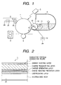
- Fig. 1 is a sectional view showing a schematic construction of an image forming apparatus according to the first embodiment of the present invention.
- Such an image forming apparatus is of reversal developing type in which an image is visualized by adhering toner as developer to an image portion of a photosensitive drum as a latent image bearing member and is an image forming apparatus of contact electrifying and one-component contact developing type.
- the image forming apparatus includes a photosensitive drum 1 as a latent image bearing member rotated at a peripheral speed of 100 mm/sec in a direction shown by the arrow A. and, around the photosensitive drum 1, along a rotational direction thereof, there are provided, in order, an electrifier 2, an exposing device 3, a developing device 4, a transferring device 5, and a fixing device 6.
- the electrifier 2 includes an elastic foam electrifying roller 20 as an electrifying member contacted with the photosensitive drum 1, and a DC high voltage power source 21 for applying electrifying bias voltage to a metal core as a conductive member of the electrifying roller 20.
- the electrifying roller 20 abut against the photosensitive drum 1 with total pressure of 1 kg and is rotatingly driven at a speed of 150 mm/sec in a direction (shown by the arrow D) opposite to a rotational direction of the photosensitive drum 1 at an abut area.
- a laser beam corresponding to image information from the exposing device 3 is illuminated onto the uniformly electrified surface of the photosensitive drum 1, thereby forming an electrostatic latent image.
- a non-laser illumination area on the surface of the photosensitive drum 1 corresponds to a non-image portion, and a laser illumination area corresponds to an image portion.
- Potential of the non-image portion is -600 V and potential of the image portion is -150 V.
- the developing device 4 has an opening portion extending in a longitudinal direction, and an elastic developing roller 10 as a developer carrying member contacted with the photosensitive drum 1 and rotated at a speed of 150 mm/sec in a direction shown by the arrow B is disposed within the opening portion.
- the developing device further includes a stripping roller or peeling roller 11 (rotated in a direction shown by the arrow C) contacted with the elastic developing roller 10, and a metallic regulating blade 12 contacted with the elastic developing roller 10 and disposed above the peeling roller 11 in a vertical direction, and non-magnetic toner as non-magnetic one-component developer is housed in the developing device 4 having these elements.
- a developing bias voltage power source 13 as a DC high voltage power source for applying developing bias to a metal core as a conductive member of the elastic developing roller 10.
- the peeling roller 11 is rotated in the direction C to carry the toner onto a surface of the elastic developing roller 10 rotated in the direction B.
- the toner carried by the elastic developing roller 10 is being passed between the elastic developing roller 10 and the regulating blade 12 urged against the elastic developing roller 10, the toner is negatively electrified by friction between the toner and the regulating blade 12 and/or the elastic developing roller 10 and a thickness of a developer layer is regulated.
- Developing bias DC voltage of -350 V is applied to the elastic developing roller 10 from the developing bias voltage power source 13.
- the developing bias DC voltage and an electric field formed from the potential on the photosensitive drum 1, in the vicinity of an abut portion (nip portion) between the photosensitive drum 1 and the elastic developing roller 10 the electrified toner is adhered to the image portion on the photosensitive drum 1, thereby visualizing the latent image.
- the toner which was not consumed in the developing station and is remaining on the elastic developing roller 10 is returned to the interior of the developing device 4 together with the elastic developing roller 10 as the elastic developing roller 10 is rotated.
- the developer on the elastic developing roller 10 is peeled by the sliding contact between the elastic developing roller 10 and the peeling roller 11 and is collected into the developing device 4.
- new toner is supplied onto the elastic developing roller 10 and is carried again to the abut area between the regulating blade 12 and the elastic developing roller 10.
- the toner image formed on the photosensitive drum 1 is transferred onto the transfer material 7 by the transferring device 5 to which positive polarity bias voltage is applied and which is disposed in a side opposite to the photosensitive drum 1 and the toner with respect to the transfer material 7.
- the drum 1 is electrified by the electrifying roller 20 and exposed by the exposing device 3 while carrying the transfer-residual toner on the photosensitive drum 1.
- the toner is supplied from the developing roller to the light portion of the drum.
- a charge injecting layer is coated on a general organic photosensitive body in which an undercoating layer, a charge injecting prevention layer, a charge generating layer and a charge transporting layer are successively coated on an aluminium base substrate in a superimposed fashion.
- the charge injecting layer is formed by mixing and dispersing SnO 2 super-fine particles as conductive particles (having a diameter of about 0.03 ⁇ m), lubricating agent such as Teflon and polymerization starting agent into acrylic resin of photo-curable type and thereafter (after coating) by effecting film-formation by means of a photo-curing method.
- a volume resistance value of the charge injecting layer is preferably within a range from 1 ⁇ 10 9 ( ⁇ cm) to 1 ⁇ 10 14 ( ⁇ cm). Further, even when the charge injecting layer as is in the illustrated embodiment is not provided, for example, if the charge transporting layer has a resistance value within the above-mentioned range, the similar effect can be achieved. Furthermore, even when an amorphous silicon photosensitive body having volume resistance (of surface layer) of about 10 13 ( ⁇ cm) is used, the similar effect can be achieved.
- the toner has a spherical or cone shape and weight mean particle diameter is preferably 10 ⁇ m or less (more preferably, 4 ⁇ m to 8 ⁇ m).
- weight mean particle diameter is preferably 10 ⁇ m or less (more preferably, 4 ⁇ m to 8 ⁇ m).
- a value of shape coefficient SF-1 as index for spherical degree is preferably 100 to 160 and a value of shape coefficient SF-2 is preferably 100 to 140.
- the shape coefficient SF-1 and the shape coefficient SF-2 of the toner according to the illustrated embodiment are defined as values obtained by sampling 100 toner images magnified by 500 times by using FE-SEM (S-800) manufactured by HITACHI Co., Ltd.
- SF - 1 ⁇ (MXLNG) 2 / AREA ⁇ ⁇ (n / 4) ⁇ 100
- SF - 2 ⁇ (PERI) 2 / AREA ⁇ ⁇ (1 / 4 ⁇ ) ⁇ 100
- AREA is a toner projection area
- MXLNG is an absolute maximum length
- PERI is a peripheral length.
- the shape coefficient SF-1 of the toner indicates degree of roundness of the toner particle, and, as the value thereof increased, the toner particle gradually becomes non-fixed from the sphere.
- the value SF-2 indicates degree of unevenness of the toner particle, and, as the value thereof increased, unevenness of the toner surface becomes more noticeable.
- S is a standard deviation value in the number distribution of the powder particles and D 1 is a number mean particle diameter (mean particle diameter by weight: ⁇ m) of the powder particles.
- D 1 is a number mean particle diameter (mean particle diameter by weight: ⁇ m) of the powder particles.
- weight mean particle diameter (mean particle diameter by number) is below 4 ⁇ m, since a reflection force (or mirroring force) is increased to reduce transferring efficiency, a number of transfer-residual toner particles on the photosensitive drum increases; whereas, if the weight mean particle diameter is greater than 10 ⁇ m, when fine dots are visualized, the latent image may not be reproduced.
- the value SF-1 is selected to 130
- the value SF-2 is selected to 120
- the weight means particle diameter is selected to about 7 ⁇ m
- the fluctuation coefficient in the number distribution is selected to 20%.
- an elastic roller having a diameter of 12 mm and Asker C hardness of 30° and constituted by coating an elastic layer made of continuous foam material on a metal core (electrode) made of stainless steel and having a diameter of 6 mm was used. Further, the electrifying nip was selected to 4 mm.
- the elastic layer is formed by heating an urethane layer obtained by uniformly dispersing conductive compounding agent such as foaming agent and carbon black thereby to achieve vulcanization and foaming and thereafter by polishing a surface if necessary.
- the electrifying roller must be contacted with the photosensitive drum sufficiently to electrify the surface of the photosensitive drum.
- the abut area between the photosensitive drum and the electrifying roller is constituted by an elastic body such as a rubber layer or a foam layer.
- the elastic body preferably has Asker C hardness of 25° to 50°.
- the material of the electrifying roller is not particularly limited and may be obtained by dispersing conductive substance such as carbon black or metal oxide into rubber (generally used) such as EPDM, urethane, NBR, silicone rubber or IR. Further, in place of the fact that the conductive substance is dispersed, ion conductive elastic layer may be used.
- the electrifying roller is rotated with speed difference with respect to the photosensitive drum at the abut area therebetween and that the electrifying roller is rotated, at the electrifying nip, in a counter direction opposite to the rotational direction of the photosensitive drum.
- the reason is that, sufficient contact chance between the photosensitive drum and the electrifying roller must be maintained in order to electrify the photosensitive drum well uniformly at the electrifying nip.
- the transfer-residual toner or any toner remaining on the photosensitive drum upon occurrence of sheet jam reaches the electrifying nip, the transfer-residual toner is returned to negative polarity by frictional agitation at the nip and the previous image pattern can be made even.
- an elastic roller having a total diameter of 16 mm and obtained by molding an elastic body on a conductive metal core (electrode) having a diameter of 8 mm and made of stainless steel was used.
- the elastic body includes has a two-layer structure comprised of an undercoating layer obtained by dispersing carbon black into silicone rubber and a surface layer made of polyamide resin and having a thickness of about 10 ⁇ m and has Asker C hardness of about 350° and dynamic coefficient of friction of about 0.1.
- the developing nip was selected to 2 mm.
- the hardness of the developing roller is desirably 25° to 50°. If the hardness is too small, since the shape of the developing roller becomes unstable, the given contacting condition is not always obtained, thereby causing uneven toner carrying amount. On the other hand, if the hardness is too great, the developing nip cannot be maintained well or deterioration of the toner will be promoted at the developing nip.
- surface roughness of the elastic developing roller 10 relates to the particle diameter of the toner used.
- the toner particle diameter of 7 ⁇ m (weight mean particle diameter) ten-point mean roughness Rz of 3 to 15 ⁇ m is desirable. If the roughness is smaller than 3 ⁇ m, the adequate toner carrying force cannot be obtained; whereas, if the roughness is greater than 15 ⁇ m, when the latent image on the photosensitive drum 1 is visualized as the toner image, unevenness on the elastic developing roller 10 may affect an influence upon the image quality.
- dynamic coefficient ⁇ of friction of the surface of the elastic developing roller 10 is preferably 0.02 to 0.8 and more preferably 0.02 to 0.4 (obtained by the following measuring method). If the dynamic coefficient of friction is too great, there will arise various problems such as excessive electrification or poor peeling; whereas, if the dynamic coefficient of friction is too small, the toner carrying amount becomes insufficient.
- the measuring method for the dynamic coefficient of friction is a method for measuring the surface of the elastic developing roller 10 by using a stainless thin plate.
- the reason for measuring the dynamic coefficient of friction of the surface of the elastic developing roller 10 contacted with stainless thin plate is that, since the photosensitive drum 1 utilizes the photosensitive layer having a thickness of several tens of ⁇ m coated on the aluminium substrate and the stainless metal plate is used as the regulating blade in the illustrated embodiment, it is considered that the dynamic coefficient of friction of the surface of the elastic developing roller 10 with respect to the stainless thin plate is proper in comparison with the actual condition.
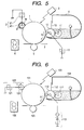
- a measuring device is shown in Fig. 3.
- the stainless thin plate having a thickness of 0.03 mm and having one end connected to a weight W1 of 100 grams and the other end connected to a digital force gauge (which is adjusted to zero value when the weight W1 and the stainless thin plate are not loaded) is set on the surface of the elastic developing roller 10 so that an angle e shown in Fig. 3 becomes 45°.
- the elastic developing roller 10 is rotated in a direction shown by the arrow R, and a sliding force between the elastic developing roller 10 and the stainless thin plate in this case is measured by the digital force gauge.
- ⁇ is dynamic coefficient of friction
- ⁇ is the angle shown in Fig. 3
- W is the sum of W1 and W2
- W1 is a weight of the weight
- W2 is a weight of the stainless thin plate
- F is a measurement value of the digital force gauge.
- the elastic body is not particularly limited to the two-layer structure but may have a single layer or three or more layers. Further, similar to the electrifying roller, the material of the elastic body is not particularly limited but may be rubber or resin generally used.
- the reason why the actual resistance value is used as a condition of resistance value is that, if the resistance value is defined by volume resistance, the resistance values between the rollers and the photosensitive drum are varied in dependence upon the roller diameters and/or thickness of the toner layer. It is preferable that a first resistance value between the metal core of the electrifying roller and the surface of the drum is set to electrify the drum surface effectively, and a second resistance value between the metal core of the developing roller and the toner layer is set to be greater than the first resistance value in order to prevent the electrification of the drum surface.
- the electrifying roller is closely urged against an aluminium drum (having a diameter of 30 mm in the illustrated embodiment) having the same diameter as that of the used photosensitive drum to apply load (total pressure of 1 kg in the illustrated embodiment) onto the electrifying roller during the image formation.
- the aluminium drum is rotated at a peripheral speed of 100 mm/sec and the electrifying roller is rotated at a speed of 50 mm/sec in the counter direction (at the electrifying nip), and voltage (-600 V in the illustrated embodiment) is actually applied to the electrifying roller, and a resistance value (referred to as "resistance value of electrifying nip") between the electrifying roller and the aluminium drum is measured.
- the developing roller carrying the toner having the same amount as that in the image formation is urged against a surface of an aluminium drum (having a diameter of 30 mm in the illustrated embodiment) having the same diameter as that of the used photosensitive drum. Then, the developing roller is closely urged against the aluminium drum to apply load (total pressure of 1.5 kg in the illustrated embodiment) onto the developing roller during the image formation.
- the aluminium drum is rotated at a peripheral speed of 100 mm/sec and the developing roller is rotated at a speed of 150 mm/sec in the same direction (at the electrifying nip), and voltage (-350 V in the illustrated embodiment) is actually applied to the developing roller, and a resistance value (referred to as "resistance value of developing nip") between the developing roller and the aluminium drum is measured.
- the resistance value of the electrifying nip is greater than 1 ⁇ 10 5 ⁇
- the surface potential of the photosensitive drum at the exposed position was -570 V thereby to cause the poor electrification ( ⁇ in Fig. 4).
- the greater the residence value the smaller the surface potential of the photosensitive drum.
- the resistance value of the electrifying nip was smaller than 1 ⁇ 10 4 ⁇
- the surface potential of the photosensitive drum at the exposing position could be electrified to about -600 V. The reason is that, if the resistance value of the electrifying nip is great, adequate electrification cannot be achieved for short electrifying nip passing time (about several 10 msec in the illustrated embodiment).
- the resistance value of the developing nip was smaller than 1 ⁇ 10 6 ⁇ , the surface potential of the photosensitive drum after passing the developing nip was changed from the previous one ( ⁇ in Fig. 4); whereas, when the resistance value of the developing nip was greater than 1 ⁇ 10 7 ⁇ , the surface potentials of the photosensitive drum before and after the developing nip were not changed. The reason is that, if the resistance value is small, the photosensitive drum is re-electrified during the developing nip passing time (about several 10 msec in the illustrated embodiment).
- a range capable of preventing the poor electrification in the image formation and preventing the re-electrification in the developing nip is defined by the fact that the resistance value between the electrifying roller and the aluminium drum is smaller than 10 5 ( ⁇ ) and the resistance value between the developing roller and the aluminium drum is greater than 10 7 ( ⁇ ) in the above-mentioned measuring method.
- the power supplies can be made compact.
- the developing roller abuts against the photosensitive drum, the toner positively electrified in the electrifying nip can be collected simultaneously with the developing, with the result that any cleaner can be omitted. Further, in the contact developing system, since a distance between the developing electrode and the electrostatic latent image is short, high quality image output corresponding to the latent image can be obtained.
- an image forming apparatus which can achieve high quality image output and which can be made compact and simplified and adapt to the environment can be provided.
- an image forming apparatus in which electrification promoting particles are disposed between the electrifying roller and the photosensitive drum in order to effect more stable electrification by means of the electrifying nip.
- Fig. 5 is a sectional view showing a schematic construction of the image forming apparatus according to the second embodiment.
- the second embodiment is characterized in that conductive electrification promoting particles exist between the electrifying roller 20 and the photosensitive drum 1.
- conductive electrification promoting particles exist between the electrifying roller 20 and the photosensitive drum 1.
- the electrification promoting particles are previously coated on the electrifying roller 20, and, thereafter, the particles is gradually supplied onto the photosensitive drum 1 from the developing device 4 by externally adding the electrification promoting particles to the toner.
- the electrification promoting particles externally added to the toner are adhered to the photosensitive drum 1 together with the toner. Further, the weak-positively electrified electrification promoting particles are also adhered to the non-image portion on the photosensitive drum 1 by an influence of an electric field. (As will be described later, since some of the electrification promoting particles are formed from metal oxide, they may be conductive or weal-positively electrified by friction in the electrifying nip and the developing nip.) Namely, the electrification promoting particles are always supplied onto the photosensitive drum 1 little by little.
- the negatively electrified toner Upon reaching to the transferring station, the negatively electrified toner is positively transferred onto the transfer material by the electric field.
- the conductive or weal-positively electrified electrification promoting particles are not positively transferred onto the transfer material by the electric field, a very small amount of the particles is physically adhered to the transfer material by unevenness on the surface of the transfer material and/or adhering ability.
- the particles are used for electrifying the surface of the photosensitive drum.
- the excessive particles which were not held by the electrifying roller 20 are adhered to the photosensitive drum 1 and are passed through the electrifying nip and the exposing portion and reach the developing nip.
- the electrification promoting particles carried to the developing nip are collected in the developing nip at an area corresponding to the image portion of the photosensitive drum 1 and are passed through the developing nip at an area corresponding to the non-image portion of the photosensitive drum 1. The latter particles are carried through the transferring portion and the electrifying portion again.
- the electrification promoting particles previously coated on the electrifying roller 20 and externally added to the toner in the developing device 4
- conductive zinc oxide particles having specific resistance of 10 7 ( ⁇ cm) and mean particle diameter of 1.5 ⁇ m are used.
- the electrification promoting particles exist not only in a primary particulate condition but also in a condition in which secondary particules are aggregated, there is no particular problem.
- the particle diameter is defined as mean particle diameter of aggregation.
- 100 or more particles are sampled by using an optical or electronic microscope, and volume grain distribution is calculated on the basis of a horizontal maximum length, and the particle diameter is determined by 50% mean particle diameter.
- the resistance value is measured by a tablet method and is sought by normalization. That is to say, powder specimen of about 0.5 gram is housed in a cylinder having a bottom area of 2.26 cm 2 , and a resistance value of the specimen is measured by applying pressure of 15 kg to upper and lower electrodes and applying voltage of 100 V to the electrodes, and, thereafter, the resistivity is calculated by normalizing the measured value.
- the specific resistance value in the present invention is smaller than 10 12 ( ⁇ cm) to obtain adequate electrifying ability, and preferably smaller than 10 10 ( ⁇ cm).
- the electrification promoting particles are preferably transparent or white not to prevent the exposure. Further, in consideration of the fact that part of the electrification promoting particles on the photosensitive drum may be adhered to the transfer material during the transferring, the electrification promoting particles are desirably transparent or white.
- the present invention is not limited to such an example, but, various conductive particles such as conductive inorganic particles made of metal oxide such as alumina or mixture with organic substance or surface-treated particles. Particularly, since many of metal oxides are white, they can be used easily.
- the number of the electrification promoting particles in the electrifying nip is desirably 500 to 500000/mm 2 on the photosensitive drum. According to the Inventor's tests, it was fond that, when such number is smaller than 500/mm 2 , contact unevenness in the electrifying nip becomes noticeable to cause poor image, and, when such number is grater than 500000/mm 2 , the particles on the photosensitive drum become too excessive, thereby causing poor exposure amount and/or exposure trouble.
- the electrifying condition and the developing condition during the actual image formation are evaluated by using the measuring method explained in connection with the first embodiment.
- the same result as the first embodiment was obtained. That is to say, when the resistance value of the electrifying nip is greater than 1 ⁇ 10 5 ⁇ , poor electrification occurred, and, when the resistance value of the developing nip is smaller than 1 ⁇ 10 6 ⁇ , the re-electrification occurred in the developing nip thereby to distort the. electrostatic latent image. It was found that, when the resistance value of the electrifying nip is below 1 ⁇ 10 5 ⁇ and the resistance value of the developing nip is greater than 1 ⁇ 10 7 ⁇ , no problem arise in the electrifying portion and the developing portion.
- the illustrated embodiment even when the electrification promoting particles exist in the electrifying nip and the developing nip, by setting the resistance value of the electrifying nip and the resistance value of the developing nip to the above-mentioned conditions, poor electrification and re-electrification in the developing nip can be prevented. Further, more uniform electrification can be achieved and the torque can be reduced.
- the supplying method for supplying the electrification promoting particles to the electrifying nip is not limited to the illustrated embodiment.
- a block made of the electrification promoting particles may be urged against the electrifying roller to supply the particles to the roller by gradually scraping the block as the electrifying roller is rotated.
- the present invention can be applied to an image forming apparatus having a cleaner. Even when electrification promoting particles are used, since the electrification promoting particle has a particle diameter smaller than the toner particle, some of the electrification promoting particles can pass through between the cleaning member and the photosensitive drum to be supplied to the electrifying nip.
- the latent image bearing member can be prevented from being re-electrified in the developing nip, and cleaning simultaneous with developing can be effected, and high quality image formation can be effected.
- the present invention provides an image forming apparatus comprising an image bearing member, an electrostatic image forming device adapted to form an electrostatic image on the image bearing member and including an electrifying member contacted with the image bearing member to electrify the image bearing member, the electrifying member having a first conductive member to which voltage is applied, and a developer carrying member cooperating with the image bearing member to form a nip therebetween and adapted to carry developer to the nip and to develop the electrostatic image with the developer and having a second conductive member to which voltage is applied, and wherein a resistance value between the second conductive member and a developer layer of the developer carried on the developer carrying member is greater than a resistance value between the first conductive member and a surface of the image bearing member.
Landscapes
- Physics & Mathematics (AREA)
- General Physics & Mathematics (AREA)
- Engineering & Computer Science (AREA)
- Plasma & Fusion (AREA)
- Dry Development In Electrophotography (AREA)
- Electrostatic Charge, Transfer And Separation In Electrography (AREA)
- Developing Agents For Electrophotography (AREA)
- Photoreceptors In Electrophotography (AREA)
Abstract
Description
Furthermore, even when an amorphous silicon photosensitive body having volume resistance (of surface layer) of about 1013 (Ω·cm) is used, the similar effect can be achieved.
Claims (29)
- An image forming apparatus comprising:an image bearing member;electrostatic image forming means adapted to form an electrostatic image on said image bearing member and including an electrifying member contacted with said image bearing member to electrify said image bearing member, said electrifying member having a first conductive member to which voltage is applied; anda developer carrying member cooperating with said image bearing member to form a nip therebetween and adapted to carry developer to said nip and to develop the electrostatic image with the developer and having a second conductive member to which voltage is applied; and whereina resistance value between said second conductive member and a developer layer of the developer carried on said developer carrying member is greater than a resistance value between said first conductive member and a surface of said image bearing member.
- An image forming apparatus according to claim 1, wherein said electrifying member has an elastic body covering said first conductive member.
- An image forming apparatus according to claim 2, wherein said first conductive member is a metal core.
- An image forming apparatus according to claim 1, wherein said developer carrying member has an elastic body covering said second conductive member.
- An image forming apparatus according to claim 4, wherein said second conductive member is a metal core.
- An image forming apparatus according to claim 1, wherein the resistance value between said second conductive member and the developer layer is greater than 107 Ω.
- An image forming apparatus according to claim 6, wherein the resistance value between said first conductive member and the surface of said image bearing member is smaller than 105 Ω.
- An image forming apparatus according to claim 1 or 6, wherein the voltage applied to said second conductive member is DC voltage.
- An image forming apparatus according to claim 1 or 6, wherein said developer carrying member can effect a developing operation and, at the same time, can clean the developer from said image bearing member.
- An image forming apparatus according to claim 1 or 7, wherein said electrifying member has an elastic body for forming an electrifying nip between said electrifying member and said image bearing member, and conductive particles are provided in said electrifying nip, and the resistance value between said first conductive member and the surface of said image bearing member is a resistance value between said first conductive member and a particle layer of the conductive particles.
- An image forming apparatus according to claim 10. wherein a resistance value of the particle layer of the conductive particles is smaller than 1012 Ω.
- An image forming apparatus according to claim 10, wherein said developer carrying member can carry the conductive particles, and the conductive particles is supplied from said developer carrying member to said image bearing member.
- An image forming apparatus according to claim 1, wherein said electrifying member injection-electrifies said image bearing member.
- An image forming apparatus according to claim 1, wherein said image bearing member has a surface layer of 1 x 10⁹ to 1 × 10¹⁴ Ω·cm.
- An image forming apparatus according to claim 1, wherein the developer has SF-1 of 100 to 160 and SF-2 of 100 to 140.
- An image forming apparatus comprising:an image bearing member;electrostatic image forming means adapted to form an electrostatic image on said image bearing member and including an electrifying member contacted with said image bearing member to electrify said image bearing member, said electrifying member having a first conductive member to which voltage is applied; anda developer carrying member cooperating with said image bearing member to form a nip therebetween and adapted to carry developer to said nip and to develop the electrostatic image with the developer and having a second conductive member to which voltage is applied; and whereina resistance value between said second conductive member and a developer layer of the developer carried on said developer carrying member is greater than 107 Ω.
- An image forming apparatus according to claim 16, wherein said electrifying member has an elastic body covering said first conductive member.
- An image forming apparatus according to claim 17, wherein said first conductive member is a metal core.
- An image forming apparatus according to claim 16, wherein said developer carrying member has an elastic body covering said second conductive member.
- An image forming apparatus according to claim 19, wherein said second conductive member is a metal core.
- An image forming apparatus according to claim 16. wherein the resistance value between said first conductive member and the surface of said image bearing member is smaller than 105 Ω.
- An image forming apparatus according to claim 16, wherein the voltage applied to said second conductive member is DC voltage.
- An image forming apparatus according to claim 16, wherein said developer carrying member can effect a developing operation and at the same time, can clean the developer from said image bearing member.
- An image forming apparatus according to claim 16 or 21, wherein said electrifying member has an elastic body for forming an electrifying nip between said electrifying member and said image bearing member, and conductive particles are provided in said electrifying nip, and the resistance value between said first conductive member and the surface of said image bearing member is a resistance value between said first conductive member and a particle layer of the conductive particles.
- An image forming apparatus according to claim 24, wherein a resistance value of the particle layer of the conductive particles is smaller than 1012 Ω.
- An image forming apparatus according to claim 24, wherein said developer carrying member can carry the conductive particles, and the conductive particles is supplied from said developer carrying member to said image bearing member.
- An image forming apparatus according to claim 16, wherein said electrifying member injection-electrifies said image bearing member.
- An image forming apparatus according to claim 16, wherein said image bearing member has a surface layer of 1 x 10⁹ to 1 × 10¹⁴ Ω·cm.
- An image forming apparatus according to claim 16, wherein the developer has SF-1 of 100 to 160 and SF-2 of 100 to 140.
Applications Claiming Priority (2)
| Application Number | Priority Date | Filing Date | Title |
|---|---|---|---|
| JP2000204468 | 2000-07-06 | ||
| JP2000204468A JP2002023480A (en) | 2000-07-06 | 2000-07-06 | Image forming device |
Publications (2)
| Publication Number | Publication Date |
|---|---|
| EP1170640A2 true EP1170640A2 (en) | 2002-01-09 |
| EP1170640A3 EP1170640A3 (en) | 2004-11-24 |
Family
ID=18701724
Family Applications (1)
| Application Number | Title | Priority Date | Filing Date |
|---|---|---|---|
| EP01116313A Withdrawn EP1170640A3 (en) | 2000-07-06 | 2001-07-05 | Image forming apparatus |
Country Status (3)
| Country | Link |
|---|---|
| US (1) | US6564027B2 (en) |
| EP (1) | EP1170640A3 (en) |
| JP (1) | JP2002023480A (en) |
Cited By (2)
| Publication number | Priority date | Publication date | Assignee | Title |
|---|---|---|---|---|
| WO2003087954A1 (en) * | 2002-04-12 | 2003-10-23 | Bridgestone Corporation | Conductive roller and imaging apparatus |
| EP3026495A1 (en) * | 2014-11-28 | 2016-06-01 | Canon Kabushiki Kaisha | Electroconductive member for electrophotography, process cartridge, and electrophotographic image-forming apparatus |
Families Citing this family (7)
| Publication number | Priority date | Publication date | Assignee | Title |
|---|---|---|---|---|
| US6821701B2 (en) * | 2001-04-03 | 2004-11-23 | Seiko Epson Corporation | Toner and image forming apparatus |
| JP2007114757A (en) * | 2005-09-21 | 2007-05-10 | Canon Inc | Image forming apparatus |
| JP4871682B2 (en) * | 2005-09-21 | 2012-02-08 | キヤノン株式会社 | Image forming apparatus |
| JP2007206482A (en) * | 2006-02-03 | 2007-08-16 | Canon Inc | Image forming method, non-magnetic one-component developer, image forming apparatus and process cartridge |
| JP5207702B2 (en) | 2006-10-20 | 2013-06-12 | キヤノン株式会社 | Image forming apparatus |
| JP4402137B2 (en) * | 2007-06-29 | 2010-01-20 | キヤノン株式会社 | Image forming apparatus, developing device and cartridge |
| CN101981517B (en) * | 2008-04-10 | 2013-03-13 | 佳能株式会社 | Image formation device |
Citations (4)
| Publication number | Priority date | Publication date | Assignee | Title |
|---|---|---|---|---|
| EP0540341A2 (en) | 1991-10-30 | 1993-05-05 | Oki Electric Industry Company, Limited | Apparatus for and method of forming image |
| EP0844536A2 (en) | 1996-11-26 | 1998-05-27 | Canon Kabushiki Kaisha | Image forming method |
| US6002900A (en) | 1997-06-13 | 1999-12-14 | Canon Kabushiki Kaisha | Image forming method, image forming apparatus and process cartridge |
| EP0977096A2 (en) | 1998-07-28 | 2000-02-02 | Tokai Rubber Industries, Ltd. | Conductive roll |
Family Cites Families (7)
| Publication number | Priority date | Publication date | Assignee | Title |
|---|---|---|---|---|
| EP0280542B1 (en) * | 1987-02-26 | 1994-11-02 | Canon Kabushiki Kaisha | An image forming apparatus |
| US5179414A (en) * | 1991-01-22 | 1993-01-12 | Compag Computer Corporation | Apparatus for developing an image on a photoconductive surface |
| US5255057A (en) * | 1992-05-29 | 1993-10-19 | Eastman Kodak Company | Gray scale monocomponent nonmagnetic development system |
| EP0619530B1 (en) | 1993-03-31 | 1999-11-03 | Canon Kabushiki Kaisha | Developing apparatus using elastic blade |
| TW287263B (en) * | 1994-06-22 | 1996-10-01 | Canon Kk | |
| JPH0844152A (en) * | 1994-07-28 | 1996-02-16 | Canon Inc | Charging member, charging device, image forming apparatus, and process cartridge |
| JP3292155B2 (en) * | 1998-09-04 | 2002-06-17 | キヤノン株式会社 | Image forming device |
-
2000
- 2000-07-06 JP JP2000204468A patent/JP2002023480A/en not_active Withdrawn
-
2001
- 2001-07-05 US US09/897,928 patent/US6564027B2/en not_active Expired - Lifetime
- 2001-07-05 EP EP01116313A patent/EP1170640A3/en not_active Withdrawn
Patent Citations (4)
| Publication number | Priority date | Publication date | Assignee | Title |
|---|---|---|---|---|
| EP0540341A2 (en) | 1991-10-30 | 1993-05-05 | Oki Electric Industry Company, Limited | Apparatus for and method of forming image |
| EP0844536A2 (en) | 1996-11-26 | 1998-05-27 | Canon Kabushiki Kaisha | Image forming method |
| US6002900A (en) | 1997-06-13 | 1999-12-14 | Canon Kabushiki Kaisha | Image forming method, image forming apparatus and process cartridge |
| EP0977096A2 (en) | 1998-07-28 | 2000-02-02 | Tokai Rubber Industries, Ltd. | Conductive roll |
Cited By (3)
| Publication number | Priority date | Publication date | Assignee | Title |
|---|---|---|---|---|
| WO2003087954A1 (en) * | 2002-04-12 | 2003-10-23 | Bridgestone Corporation | Conductive roller and imaging apparatus |
| EP3026495A1 (en) * | 2014-11-28 | 2016-06-01 | Canon Kabushiki Kaisha | Electroconductive member for electrophotography, process cartridge, and electrophotographic image-forming apparatus |
| US9442451B2 (en) | 2014-11-28 | 2016-09-13 | Canon Kabushiki Kaisha | Electroconductive member for electrophotography, process cartridge, and electrophotographic image-forming apparatus |
Also Published As
| Publication number | Publication date |
|---|---|
| JP2002023480A (en) | 2002-01-23 |
| US6564027B2 (en) | 2003-05-13 |
| US20020015600A1 (en) | 2002-02-07 |
| EP1170640A3 (en) | 2004-11-24 |
Similar Documents
| Publication | Publication Date | Title |
|---|---|---|
| US5311264A (en) | Developing apparatus for developing electrostatic latent image using one component developer | |
| US6594462B2 (en) | Developing apparatus using toner with conductive particles | |
| US6314257B1 (en) | Simultaneous developing/cleaning device | |
| EP1574911A1 (en) | Developing apparatus for developing under pressure and with a single component magnetic toner | |
| US6389254B2 (en) | Charging member holding charge accelerating particles in a continuous bubble | |
| US6564027B2 (en) | Image forming apparatus | |
| US6647229B2 (en) | Image forming apparatus with flexible charging member for use with spherical toner | |
| JP2001215798A (en) | Image forming device | |
| JP2002099176A (en) | Image forming device | |
| US6594461B2 (en) | Charger and image formation apparatus using the charger | |
| JP3104007B2 (en) | Developing device in image forming apparatus | |
| US6308038B1 (en) | Developing apparatus | |
| JP2002174944A (en) | Image forming device | |
| JP2002099141A (en) | Developing device and image forming apparatus provided with the same | |
| JP3253280B2 (en) | Image forming device | |
| JP3647264B2 (en) | Image forming apparatus | |
| JP2003057948A (en) | Image forming apparatus and process cartridge | |
| JPH1010863A (en) | Developing device and image forming method | |
| JP3397700B2 (en) | Charging member, charging method, charging device, image forming apparatus, and process cartridge | |
| JP2000081760A (en) | Image forming device | |
| JPH09325575A (en) | Image forming device | |
| JP3376290B2 (en) | Charging method, charging device, image forming apparatus, and process cartridge | |
| JP3513502B2 (en) | Image forming device | |
| JP2002258612A (en) | Developing device, process cartridge and image forming device | |
| JP2002207346A (en) | Image forming device |
Legal Events
| Date | Code | Title | Description |
|---|---|---|---|
| PUAI | Public reference made under article 153(3) epc to a published international application that has entered the european phase |
Free format text: ORIGINAL CODE: 0009012 |
|
| AK | Designated contracting states |
Kind code of ref document: A2 Designated state(s): AT BE CH CY DE DK ES FI FR GB GR IE IT LI LU MC NL PT SE TR |
|
| AX | Request for extension of the european patent |
Free format text: AL;LT;LV;MK;RO;SI |
|
| PUAL | Search report despatched |
Free format text: ORIGINAL CODE: 0009013 |
|
| AK | Designated contracting states |
Kind code of ref document: A3 Designated state(s): AT BE CH CY DE DK ES FI FR GB GR IE IT LI LU MC NL PT SE TR |
|
| AX | Request for extension of the european patent |
Extension state: AL LT LV MK RO SI |
|
| 17P | Request for examination filed |
Effective date: 20050401 |
|
| AKX | Designation fees paid |
Designated state(s): DE FR GB IT |
|
| 17Q | First examination report despatched |
Effective date: 20080430 |
|
| STAA | Information on the status of an ep patent application or granted ep patent |
Free format text: STATUS: THE APPLICATION HAS BEEN WITHDRAWN |
|
| 18W | Application withdrawn |
Effective date: 20110127 |