EP1168742A1 - Modulation identification device - Google Patents
Modulation identification device Download PDFInfo
- Publication number
- EP1168742A1 EP1168742A1 EP00113679A EP00113679A EP1168742A1 EP 1168742 A1 EP1168742 A1 EP 1168742A1 EP 00113679 A EP00113679 A EP 00113679A EP 00113679 A EP00113679 A EP 00113679A EP 1168742 A1 EP1168742 A1 EP 1168742A1
- Authority
- EP
- European Patent Office
- Prior art keywords
- signal
- modulation
- signal processing
- modulated
- identification device
- Prior art date
- Legal status (The legal status is an assumption and is not a legal conclusion. Google has not performed a legal analysis and makes no representation as to the accuracy of the status listed.)
- Granted
Links
Images




Classifications
-
- H—ELECTRICITY
- H04—ELECTRIC COMMUNICATION TECHNIQUE
- H04L—TRANSMISSION OF DIGITAL INFORMATION, e.g. TELEGRAPHIC COMMUNICATION
- H04L27/00—Modulated-carrier systems
- H04L27/18—Phase-modulated carrier systems, i.e. using phase-shift keying
-
- H—ELECTRICITY
- H04—ELECTRIC COMMUNICATION TECHNIQUE
- H04B—TRANSMISSION
- H04B1/00—Details of transmission systems, not covered by a single one of groups H04B3/00 - H04B13/00; Details of transmission systems not characterised by the medium used for transmission
- H04B1/06—Receivers
- H04B1/16—Circuits
-
- H—ELECTRICITY
- H04—ELECTRIC COMMUNICATION TECHNIQUE
- H04L—TRANSMISSION OF DIGITAL INFORMATION, e.g. TELEGRAPHIC COMMUNICATION
- H04L27/00—Modulated-carrier systems
- H04L27/0012—Modulated-carrier systems arrangements for identifying the type of modulation
-
- H—ELECTRICITY
- H04—ELECTRIC COMMUNICATION TECHNIQUE
- H04L—TRANSMISSION OF DIGITAL INFORMATION, e.g. TELEGRAPHIC COMMUNICATION
- H04L27/00—Modulated-carrier systems
- H04L27/32—Carrier systems characterised by combinations of two or more of the types covered by groups H04L27/02, H04L27/10, H04L27/18 or H04L27/26
- H04L27/34—Amplitude- and phase-modulated carrier systems, e.g. quadrature-amplitude modulated carrier systems
Definitions
- the present invention relates to a modulation identification device, to a software defined radio device as well as to a method for identifying the modulation type of wirelessly transmitted modulated RF signal.
- SDR devices can be reconfigured (with software downloaded either over-the-air or locally) to operate over a wide frequency band and with a variety of digital modulation formats, such as M-array, phase-shift keying (M-PSK) or M-array quadrature-amplitude-modulation (M-QAM). It is therefore desirable to have methods for a detection of multiple digital modulations. Particularly, some SDR receivers may need to determine the type of modulation without any a-priori knowledge. Further information on software-defined radio can be found in J. Mitola, "The Software Radio Architecture", IEEE Communications Magazine, vol. 33, no. 5, pages 26 to 28, May 1995.
- Nandi et al "Algorithms for Automatic Recognition of Communication Signals", IEEE Trans. Comm., vol. 46, no. 4, pages 431 to 436, April 1998 proposes two methods for modulation recognition.
- the first approach is "decision-theoretical” in the sense that it requires high-order moments of the amplitude, phase and frequency of the signals in order to extract the key features.
- the second method uses an artificial neural network. Both methods are solutions to a pattern recognition problem and require to process a large number of received symbols.
- a n-port junction device being supplied with a modulated RF signal to be detected and a second RF signal (for example from a local oscillator).
- the n-port junction device combines in a linear manner (no RF mixing units) the two input RF signals and outputs at least one RF signal (being the result of the linear combination(s)) to at least one power detector.
- the six-port technique has been known for its ability to accurately measure the scattering parameters, both amplitude and phase, of microwave networks. Instead of using heterodyne receivers a six-port receiver accomplishes direct measurements at microwave and mm-wave frequencies by extracting power levels at at least three and particularly four of the 6 ports. The imperfections of the hardware can be readily eliminated by an appropriate calibration procedure. Very accurate measurements can be made in a large dynamic range and wide frequency range.
- six-port junction receivers consist of passive microwave components such as directional couplers and power dividers as well as diode detectors. The circuit can be easily integrated as MHMIC or MMIC. The known receiver performs direct phase/amplitude demodulation at microwave and mm-wave frequencies.
- correlator circuit for a six-port receiver is known.
- the received signal is summed up with a local oscillator signal at various phase angles, wherein the phase rotation between the local oscillator and RF signals is carried out separately from the summing of the correlator outputs.
- a modulation identification device having a first input for a modulated RF signal to be identified and a second input for a second RF signal having a frequency essentially corresponding to the carrier frequency of the modulated RF signal.
- the modulation identification device furthermore has an output for a flag indicating a modulation type identified.
- the device comprises a n-port junction, n being an integer equal to or larger than three.
- the n-port junction is supplied to the modulated RF signal and the second RF signal and is designed to output at least one third RF signal to at least one power detector.
- a signal processing unit is provided to process the output of the power detector to generate the at least one flag.
- a unit for averaging at least one branch of the output of the power detector over a predetermined number of symbols can be provided.
- the signal processing unit can comprise at least one comparison unit for comparing a processed output of the at least one power detector with at least one predetermined threshold.
- the at least one predetermined threshold can be calculated on the basis of at least one relative power ratio.
- the relative power ratio is the ratio of the current processed output of the at least one power detector and an average processed output of the at least one power detector.
- the signal processing unit can furthermore comprise at least one counter for counting the number of hits for which the processed output of the at least power detector satisfies at least one predetermined comparison condition, the comparison condition being calculated based on the at least one threshold.
- the signal processing unit can comprise a calculation unit for calculating a probability for each modulation type to be identified on the basis of the number of hits.
- the signal processing unit can be designed to output a flag for an identified modulation type in case the corresponding calculated probability exceeds a predetermined probability threshold.
- the signal processing unit can be provided with an input for a-priori information on the symbol duration of the modulated RF signal.
- a software defined radio device comprising a modulation identification device as set forth above.
- a method for identifying the modulation type of a wirelessly transmitted modulated RF signal is proposed.
- the modulated RF signal (to be identified) and a second RF signal having a frequency essentially corresponding to the carrier frequency of the modulated RF signal are supplied to the input of a n-port junction outputting at least one RF signal, n being an integer larger than three.
- the at least one output RF signal of the n-port junction is processed to generate at least one flag indicating the identified modulation type of the modulated RF signal.
- At least one branch of the output of the n-port junction can be averaged over a predetermined number of symbols.
- the step of signal processing can comprise the step of comparing a processed output of the n-port junction with at least one predetermined threshold.
- the step of signal processing can furthermore comprise the step of counting the number of hits for which the processed output of the n-port junction satisfies at least one predetermined comparison condition.
- the step of signal processing can furthermore comprise the step of calculating a probability for each modulation type to be identified on the basis of the number of hits.
- the step of signal processing can furthermore comprise the step of outputting a flag for a identified modulation type in case the corresponding calculated probability exceeds a predetermined probability threshold.
- a n-port junction device having two RF inputs and at least one RF output for identifying the modulation type of a wireless transmitted modulated RF signal supplied to a first of the two RF inputs is used.
- n being an integer larger than three, the modulation type can be identified without a-priori knowledge of the modulation type.
- a modulated RF signal 2 is input into the modulation identification device 1 and the modulation identification device 1 outputs a flag 10 for a detected modulation scheme which has been used for the transmission of the modulated RF signal input in the modulation identification device 1.
- a second RF signal having a frequency essentially corresponding to the carrier frequency of the modulated RF signal is input 3 to the modulation identification device 1.
- the modulation identification device 1 generally comprises two portions, the first part 5 comprising an n-port junction 17 (n being an integer larger than two) and at least one power detector 18 detecting the power of RF output signals of the n-port junction 17.
- the n-port junction 17 combines the two RF signals 2, 3 in a linear manner (without RF mixing or other non-linear processing) and outputs RF signals to the power detector(s) 18.
- the at least one power detector 18 supplies a power detection signal to a signal processing unit 6. Additionally the signal processing unit 6 can be provided with information 4 regarding the symbol duration of the modulated RF signal 2. The signal processing unit 6 can perform digital, analog or hybrid (both digital and analog) processing. Depending on the result of the signal processing of the signal processing unit 6, a flag "raised" for the modulation scheme, which is assumed to be used for the transmission of the modulated RF signal 2.
- such a modulation identification device can detect a modulation type without a-priori information on the modulation scheme used for the transmission of the modulated RF signal 2.
- a modulation identification device can satisfy the following requirements:
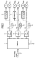
- Figure 2 shows a first part of the signal path of a modulation identification device 1 as shown in figure 1.
- the n-port junction device 17 is a five-port junction 7 having two inputs 2, 3 and three outputs.
- the output signals of the five-port junction 7 are respectively passed through a low-pass-filter 8.
- the low-pass-filtered output signals of the five-port junction device 7 can be optionally A/D-converted 16.
- the three low-pass-filtered output signals P 1 , P 2 , P 3 are split up respectively in two branches, wherein a first branch of the output signals is passed through a averaging unit 9 for averaging the corresponding low-pass-filtered signal P 1 , P 2 or P 3 over a predetermined number of symbols to generate respectively a averaged signal P 10 , P 20 and P 30 . Therefore, in the case of a five-port junction device 7 having three outputs, in total six signals can be used for the further processing shown in figure 3, i.e. the current signals P 1 , P 2 and P 3 as well as the average signals P 10 , P 20 and P 30 .
- Figure 3 shows the signal processing following the signal path of figure 2 and which takes essentially place in the signal processing unit 6.
- the current and averaged output signals P 1 , P 10 , P 2 , P 20 , P 3 and P 30 are used to set up conditions by calculated threshold values TS1, TS2, TS3, TS4. For each received symbol it is checked whether the current low-pass-filtered power signals P 1 and P 3 satisfy respectively the following condition: TS1 ⁇ p 1 ⁇ TS2 TS3 ⁇ p 3 ⁇ TS4
- the digital processing unit 6 comprises a counter 13 counting the number n hit of so-called hits, i.e. the number of symbols for which the corresponding threshold condition had been satisfied by the corresponding current signal P 1 or P 3 .
- the number of hits is forwarded to a probability calculation and decision logic 15 in the signal processing unit 6.
- a counter for counting the total number of received symbols n sym 14 is provided supplying the corresponding information n sym to the probability calculation and decision logic 15.
- the probability calculation and decision logic 15 performs a probability calculation and a decision logic process which will be explained later on. Based on the probability calculation and the decision logic in the unit 15 the corresponding flag 10, i.e. the flag for which the decision based on the probability calculation had a positive result, is "raised".
- the modulated RF signal to be identified and the LO signal are supplied to the input of the n-port junction device.
- three RF outputs are provided, which are supplied to power detectors detecting the power levels of p 1 , p 2 and p 3 . Those signals are passing through low-pass-filters.
- These DC signals may be A/D converted.
- the DC signals are respectively split in two branches whereoin one branch is analog averaged and supplied together with the non-averaged signals to a analog/digital conversion unit.
- this six informations are further processed by analog or digital means of the signal processing unit.
- Signal denoted with “1” is sufficient for setting comparison thresholds for mQAM signals, where “m” takes values of 16, 64 and 256.
- Signals denoted by “3”, “4" and “5" are required for setting thresholds for nPSK type of signals, where “n” takes values of 2, 4, 8 or 16.
- Typical examples of the 16QAM and 64QAM modulation schemes are presented in figure 5a.
- Relative power ratios (of the average power and present power at "five-port" receiver port (p 1 ), are playing a major role in definition of the decision thresholds.
- Relative power levels (p 1 ) are presented in figure 5a for 16QAM and 64QAM.
- Thresholds TS1 is placed at one half of the distance between highest magnitude level and one the first intermediate lower magnitude level for related modulation. Threshold TS2 is higher than highest magnitude level for the same distance.
- current p 1 value has to be compared with related sets of TS1 and TS2 thresholds, and if the "hit" is achieved, a counter for related type of mQAM modulation is incremented.
- Thresholds TS3 and TS4 are determined by actual power level (p 2 ), average power level of the input signal and detector device specific constants.
- TS 3 p 30 +( p 2 - p 20 )tan( ⁇ 1 )
- nonlinear thresholds may be defined in order to further improve detection sensitivity. However, additional processing is required, which does not necessarily justify improvement in sensitivity.
- P mPSK 1- 1- m ⁇ n hit 2 n sym , n hit2 - Number of hits in (p 2 p 3 ) - area
- P mQAM 1- 1- m 4 ⁇ n hit 1 n sym , n hit1 - Number of hits in p 1 - area n sym - Number of symbols
Landscapes
- Engineering & Computer Science (AREA)
- Computer Networks & Wireless Communication (AREA)
- Signal Processing (AREA)
- Digital Transmission Methods That Use Modulated Carrier Waves (AREA)
Abstract
Description
- The present invention relates to a modulation identification device, to a software defined radio device as well as to a method for identifying the modulation type of wirelessly transmitted modulated RF signal.
- Software defined radio (SDR) devices can be reconfigured (with software downloaded either over-the-air or locally) to operate over a wide frequency band and with a variety of digital modulation formats, such as M-array, phase-shift keying (M-PSK) or M-array quadrature-amplitude-modulation (M-QAM). It is therefore desirable to have methods for a detection of multiple digital modulations. Particularly, some SDR receivers may need to determine the type of modulation without any a-priori knowledge. Further information on software-defined radio can be found in J. Mitola, "The Software Radio Architecture", IEEE Communications Magazine, vol. 33, no. 5, pages 26 to 28, May 1995.
- Therefore most recently, there has been a growing interest in digital modulation identification. Nandi et al, "Algorithms for Automatic Recognition of Communication Signals", IEEE Trans. Comm., vol. 46, no. 4, pages 431 to 436, April 1998 proposes two methods for modulation recognition. The first approach is "decision-theoretical" in the sense that it requires high-order moments of the amplitude, phase and frequency of the signals in order to extract the key features. The second method uses an artificial neural network. Both methods are solutions to a pattern recognition problem and require to process a large number of received symbols.
- In view of the still growing need for modulation identification methods and devices, it is the object of the present invention to propose a technique for modulation identification on the basis of a less complicated procedure.
- This object is achieved according to the present invention generally by using a n-port junction device being supplied with a modulated RF signal to be detected and a second RF signal (for example from a local oscillator). The n-port junction device combines in a linear manner (no RF mixing units) the two input RF signals and outputs at least one RF signal (being the result of the linear combination(s)) to at least one power detector.
- The six-port technique has been known for its ability to accurately measure the scattering parameters, both amplitude and phase, of microwave networks. Instead of using heterodyne receivers a six-port receiver accomplishes direct measurements at microwave and mm-wave frequencies by extracting power levels at at least three and particularly four of the 6 ports. The imperfections of the hardware can be readily eliminated by an appropriate calibration procedure. Very accurate measurements can be made in a large dynamic range and wide frequency range. six-port junction receivers consist of passive microwave components such as directional couplers and power dividers as well as diode detectors. The circuit can be easily integrated as MHMIC or MMIC. The known receiver performs direct phase/amplitude demodulation at microwave and mm-wave frequencies.
- By performing a calibration procedure the hardware imperfections such as phase error of the bridges, imbalance of the power detectors, etc. can be readily eliminated. This significantly eases the requirement of the hardware implementation and enables the six-port receiver to operate over a wide band up to mm-wave frequencies.
- According to the above cited document of Bossisio et. al. a six-port receiver concept with power dividers and 90 degrees hybrid circuits realized in distributed technology is used. The application of that known structure lies mainly in the frequency bands above 10 GHz, however, it suffers from an insufficient band width of the operation due to the inherently frequency selective nature of the 90 degrees hybrid circuits.
- From D. Maurin, Y.Xu, B.Huyart, K.Wu, M. Cuhaci, R. Bossisio "CPW Millimeter-Wave Six-Port Reflectometers using MHMIC and MMIC technologies", European Microwave Conference 1994, pp. 911-915, a wide-band topology for reflectometer used is known which is based on a distributing element approach featuring coplanar wave guide applications in the frequency range from 11 to 25 GHz.
- From V. Bilik, et al. "A new extremely wideband lumped six-port reflectometer" European Microwave Conference 1991, pp. 1473-1477 and the idea of using Wheatstone Bridges and resistive structures for reflectometer applications is known.
- From j:Li, G.Bossisio, K.Wu, "Dual tone Calibration of Six-Port Junction and its application to the six-port direct digital receiver", IEEE Transactions on Microwave Theory and Techniques, vol. 40, January 1996 a six-port reflectometer topology based on four 3dB hybrid circuits, power dividers and attenuators is known.
- From US-A-5498969 an asymmetrical topology for a reflectometer structure featuring matched detectors and one unmatched detector is known.
- From US-A-4521728 with the title "Method and six-port network for use in determining complex reflection coefficients of microwave networks" a reflectometer six-port topology is known comprising two different quadrate hybrids, phase shifter, two power dividers and one directional coupler for which the realization by a microstrip line technology is disclosed.
- From EP-A-0 805 561 a method for implementing a direct conversion receiver with a six-port junction is known. According to this known technique, modulated transmitted modulation is received by a direct conversion receiver which comprises a six-port junction. The demodulation is carried out analogically.
- From EP-A- 0 841 756 a correlator circuit for a six-port receiver is known. In this correlator circuit the received signal is summed up with a local oscillator signal at various phase angles, wherein the phase rotation between the local oscillator and RF signals is carried out separately from the summing of the correlator outputs.
- To be more specific, according to the present invention a modulation identification device having a first input for a modulated RF signal to be identified and a second input for a second RF signal having a frequency essentially corresponding to the carrier frequency of the modulated RF signal is provided. The modulation identification device furthermore has an output for a flag indicating a modulation type identified. The device comprises a n-port junction, n being an integer equal to or larger than three. The n-port junction is supplied to the modulated RF signal and the second RF signal and is designed to output at least one third RF signal to at least one power detector. A signal processing unit is provided to process the output of the power detector to generate the at least one flag.
- A unit for averaging at least one branch of the output of the power detector over a predetermined number of symbols can be provided.
- The signal processing unit can comprise at least one comparison unit for comparing a processed output of the at least one power detector with at least one predetermined threshold.
- The at least one predetermined threshold can be calculated on the basis of at least one relative power ratio. The relative power ratio is the ratio of the current processed output of the at least one power detector and an average processed output of the at least one power detector.
- The signal processing unit can furthermore comprise at least one counter for counting the number of hits for which the processed output of the at least power detector satisfies at least one predetermined comparison condition, the comparison condition being calculated based on the at least one threshold.
- The signal processing unit can comprise a calculation unit for calculating a probability for each modulation type to be identified on the basis of the number of hits.
- The signal processing unit can be designed to output a flag for an identified modulation type in case the corresponding calculated probability exceeds a predetermined probability threshold.
- The signal processing unit can be provided with an input for a-priori information on the symbol duration of the modulated RF signal.
- According to another aspect of the present invention a software defined radio device is proposed comprising a modulation identification device as set forth above.
- According to a still further aspect of the present invention a method for identifying the modulation type of a wirelessly transmitted modulated RF signal is proposed. The modulated RF signal (to be identified) and a second RF signal having a frequency essentially corresponding to the carrier frequency of the modulated RF signal are supplied to the input of a n-port junction outputting at least one RF signal, n being an integer larger than three. The at least one output RF signal of the n-port junction is processed to generate at least one flag indicating the identified modulation type of the modulated RF signal.
- At least one branch of the output of the n-port junction can be averaged over a predetermined number of symbols.
- The step of signal processing can comprise the step of comparing a processed output of the n-port junction with at least one predetermined threshold.
- The step of signal processing can furthermore comprise the step of counting the number of hits for which the processed output of the n-port junction satisfies at least one predetermined comparison condition.
- The step of signal processing can furthermore comprise the step of calculating a probability for each modulation type to be identified on the basis of the number of hits.
- The step of signal processing can furthermore comprise the step of outputting a flag for a identified modulation type in case the corresponding calculated probability exceeds a predetermined probability threshold.
- According to a still further aspect of the present invention a n-port junction device having two RF inputs and at least one RF output for identifying the modulation type of a wireless transmitted modulated RF signal supplied to a first of the two RF inputs is used. In line with this use of an n-port junction device, n being an integer larger than three, the modulation type can be identified without a-priori knowledge of the modulation type.
- Further objects, advantages and features of the present invention will become evident for the man skilled in the art when reading the following detailed description of embodiments of the present invention, taken in conjunction with the figures of the enclosed drawings.
- Figure 1 shows a schematic representation of a modulation identification device,
- Figure 2 shows a first portion of the signal path in a modulation identification device as shown in figure 1,
- Figure 3 shows a second part of the signal path and signal processing following the signal path as shown in figure 2,
- Figure 4 shows a flow chart of the signal processing,
- Figure 5a shows a table of relative power levels in the case of a 64 QAM and a 16 QAM, respectively,
- Figure 5b shows a graphical representation of the relative power levels for 64 QAM and 16 QAM,
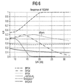
- Figure 6 shows the response of a modulation identification device according to the present invention for a 16 QAM detection versus other modulation schemes, and
- Figure 7 shows the sensitivity of a modulation detection, wherein a probability of 0.65 has been set for the flag activation.
- With reference to figure 1 a general overview of a modulation identification device according to the present invention is given. Generally speaking, a modulated
RF signal 2 is input into themodulation identification device 1 and themodulation identification device 1 outputs aflag 10 for a detected modulation scheme which has been used for the transmission of the modulated RF signal input in themodulation identification device 1. - Furthermore, a second RF signal having a frequency essentially corresponding to the carrier frequency of the modulated RF signal is
input 3 to themodulation identification device 1. - The
modulation identification device 1 generally comprises two portions, thefirst part 5 comprising an n-port junction 17 (n being an integer larger than two) and at least onepower detector 18 detecting the power of RF output signals of the n-port junction 17. As it is known from the prior art, the n-port junction 17 combines the twoRF signals - Regarding the internal structure and possible implementations of the n-port junction, reference is made explicitly to WO 99/33166 with the title "N-port direct receiver".
- The at least one
power detector 18 supplies a power detection signal to asignal processing unit 6. Additionally thesignal processing unit 6 can be provided withinformation 4 regarding the symbol duration of the modulatedRF signal 2. Thesignal processing unit 6 can perform digital, analog or hybrid (both digital and analog) processing. Depending on the result of the signal processing of thesignal processing unit 6, a flag "raised" for the modulation scheme, which is assumed to be used for the transmission of the modulatedRF signal 2. - As can be seen from the general overview of figure 1, such a modulation identification device can detect a modulation type without a-priori information on the modulation scheme used for the transmission of the modulated
RF signal 2. - Therefore, a modulation identification device according to the present invention can satisfy the following requirements:
- a) identification of modulation type can be done directly at RF frequency with minimum number of RF elements and without intermediate frequency stages,
- b) I/Q values are not necessarily calculated,
- c) the digital/analog/hybrid processing effort is acceptable, and
- d) even in severe S/N conditions phase locked modulation types can be identified with acceptable probability.
- Figure 2 shows a first part of the signal path of a
modulation identification device 1 as shown in figure 1. According to this example, the n-port junction device 17 is a five-port junction 7 having twoinputs filter 8. After the low-pass-filtering 8 the low-pass-filtered output signals of the five-port junction device 7 can be optionally A/D-converted 16. The three low-pass-filtered output signals P1, P2, P3 are split up respectively in two branches, wherein a first branch of the output signals is passed through a averagingunit 9 for averaging the corresponding low-pass-filtered signal P1, P2 or P3 over a predetermined number of symbols to generate respectively a averaged signal P10, P20 and P30. Therefore, in the case of a five-port junction device 7 having three outputs, in total six signals can be used for the further processing shown in figure 3, i.e. the current signals P1, P2 and P3 as well as the average signals P10, P20 and P30. - Figure 3 shows the signal processing following the signal path of figure 2 and which takes essentially place in the
signal processing unit 6. - As will be seen from figure 3, the current and averaged output signals P1, P10, P2, P20, P3 and P30 are used to set up conditions by calculated threshold values TS1, TS2, TS3, TS4. For each received symbol it is checked whether the current low-pass-filtered power signals P1 and P3 satisfy respectively the following condition:


- The
digital processing unit 6 comprises acounter 13 counting the number nhit of so-called hits, i.e. the number of symbols for which the corresponding threshold condition had been satisfied by the corresponding current signal P1 or P3. The number of hits is forwarded to a probability calculation anddecision logic 15 in thesignal processing unit 6. Furthermore a counter for counting the total number of receivedsymbols n sym 14 is provided supplying the corresponding information nsym to the probability calculation anddecision logic 15. The probability calculation anddecision logic 15 performs a probability calculation and a decision logic process which will be explained later on. Based on the probability calculation and the decision logic in theunit 15 the correspondingflag 10, i.e. the flag for which the decision based on the probability calculation had a positive result, is "raised". - With reference to the flow chart of figure 4 the processing according to the present invention is shortly summarized:
- In a step S1 the DC outputs representing the magnitude of linear combinations of the modulated RF signal and the second RF signal (from a local oscillator) are generated.
- In a step S2 the DC outputs (of the n-port junction) are low-pass-filtered.
- In a step S3 the low-pass-filtered power detected DC outputs are compared with pre-calculated first threshold values.
- In a step S4 the number of hits nhit of the comparison step S3 is counted over a predetermined number nsym of symbols.
- In a step S5 a probability calculation for at least one modulation type based on the number of hits of step S4 is performed.
- Finally, a flag for the modulation type is output for which the calculated probability exceeded a second threshold value.
- In the following the theoretical background of the present invention will be explained.
- The modulated RF signal to be identified and the LO signal are supplied to the input of the n-port junction device. As a result of the combination of the LO signal with different phase rotation with modulated RF signal, three RF outputs are provided, which are supplied to power detectors detecting the power levels of p1, p2 and p3. Those signals are passing through low-pass-filters. These DC signals may be A/D converted. Alternatively the DC signals are respectively split in two branches whereoin one branch is analog averaged and supplied together with the non-averaged signals to a analog/digital conversion unit. Generally, this six informations (direct signals and averaged signals) are further processed by analog or digital means of the signal processing unit. Signal denoted with "1" is sufficient for setting comparison thresholds for mQAM signals, where "m" takes values of 16, 64 and 256. Signals denoted by "3", "4" and "5" are required for setting thresholds for nPSK type of signals, where "n" takes values of 2, 4, 8 or 16.
- Typical examples of the 16QAM and 64QAM modulation schemes are presented in figure 5a. Relative power ratios (of the average power and present power at "five-port" receiver port (p1), are playing a major role in definition of the decision thresholds. Relative power levels (p1), are presented in figure 5a for 16QAM and 64QAM.
- Thresholds TS1 is placed at one half of the distance between highest magnitude level and one the first intermediate lower magnitude level for related modulation. Threshold TS2 is higher than highest magnitude level for the same distance. For all related mQAM modulations, current p1 value has to be compared with related sets of TS1 and TS2 thresholds, and if the "hit" is achieved, a counter for related type of mQAM modulation is incremented. The values of r1 and r2 relate to figure 5a.
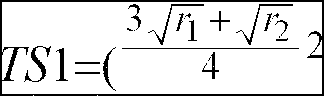

- In the following equations average power levels for p2 and p3 are presented.





- Thresholds TS3 and TS4 are determined by actual power level (p2), average power level of the input signal and detector device specific constants.
- For each phase modulation (mPSK) sets of thresholds are available.


- Note that,
"m" is related to art of "m"PSK modulation. - In table 1 possible example of angels for mPSK modulations are presented.
Table 1: Proposed threshold angles for phase modulations q=m/4 α1[°] α2[°] BPSK ½ 180 270 QPSK 1 157.5 202.5 8PSK 2 146.25 168.75 16PSK 4 140.625 151.875 - It should be denoted that very simple numerical approach for angle positioning for mPSK is proposed, in order to minimize processing efforts. Moreover, it is proposed to utilize different detection areas for mPSK modulation types or for each particular modulation art.
- Note that specific nonlinear thresholds may be defined in order to further improve detection sensitivity. However, additional processing is required, which does not necessarily justify improvement in sensitivity.
- In the following equations information expression for probability calculation is presented for both: mPSK and mQAM type of modulations.


- Note we found out that probability of 0.65 may be sufficient to "raise the flag" that modulation is locked.
- Simulation results are performed in respect to classic "five-port" structure. In all calculation ideal "five-port" structure with phase shift of 45 degrees are considered.
Table 2: Required S/N for probability of modulation identification for different modulation types Probability: P=0.65 P=0.75: P=0.85 P=0.95 Modulation: S/N
(1)S/N
(2)S/N
(1)S/N
(2)S/N
(1)S/N
(2)S/N
(1)S/N
(2)BPSK -5 -2.5 -2 0.5 1 3 4 6 QPSK 3 4 6 6.5 8 8.5 11 11.5 8PSK 7.5 11 10.5 12.5 12.5 14 15 17 16PSK 15 17 18.5 21.5 16QAM 12.5 14 14.5 16 17 17.5 19 19.5 64QAM 18 21.5 21 22.5 23 24 25 26
Claims (16)
- Modulation identification device having a first input (2) for a modulated RF signal to be identified, a second input (3) for a second RF signal having a frequency essentially corresponding to the carrier frequency of the modulated RF signal and at least one output for a flag (10) indicating a modulation type identified, wherein the device (1) comprises:- a n-port junction (17), n being an integer equal to or larger than three, being supplied with the modulated RF signal and the second RF signal and outputting at least one third RF signal to at least one power detector (18), and- a signal processing unit (6) for processing the output of the power detector (18) to generate the at least one flag (10).
- Modulation identification device according to claim 1,
characterized by
a unit (9) for averaging at least one branch of the output of the power detector (18) over a predetermined numbers of symbols before it is supplied to the signal processing unit (6). - Modulation identification device according to claim 1 or 2,
characterized in that
the signal processing unit (6) comprises at least one comparison unit (11, 12) for comparing a processed output of the at least one power detector (18) with at least one predetermined threshold. - Modulation identification device according to claim 3,
characterized in that
the at least one threshold is calculated on the basis of at least one relative power ratio, the relative power ratio being the ratio of the current processed output of the at least one power detector (18) and an average processed output of the at least one power detector (18). - Modulation identification device according to claim 3 or 4,
characterized in that
the signal processing unit (6) comprises at least one counter (13) for counting the number (nhit) of hits for which the processed output of the at least one power detector (18) satisfies at least one predetermined comparison condition, the comparison condition being based on the at least one threshold.. - Modulation identification device according to claim 5,
characterized in that
the signal processing unit (6) comprises a calculation unit (15) for calculating a probability for each modulation type to be identified on the basis of the number of hits. - Modulation identification device according to claim 6,
characterized in that
the signal processing unit (6) is designed to output a flag (10) for an identified modulation type in case the corresponding calculated probability exceeds a predetermined probability threshold. - Modulation identification device according to anyone of the preceding claims,
characterized in that
the signal processing unit (6) is provided with an input (4) for a-priori information on the symbol duration of the modulated RF signal. - Software defined radio device,
characterized in that
it comprises a modulation identification device (1) according to anyone of the preceding claims. - Method for identifying the modulation type of a wirelessly transmitted modulated RF signal,
the method comprising the following steps:- supplying (2, 3) the modulated RF signal and a second RF signal having a frequency essentially corresponding to the carrier frequency of the modulated RF signal respectively to the input of a n-port junction (5) outputting at least one RF signal, n being an integer larger than three,- signal processing (6) the at least one output RF signal of the n-port junction to generate (15) at least one flag (10) indicating the identified modulation type of the modulated RF signal. - Method according to claim 10,
characterized in that
at least one branch of the output of the n-port junction is averaged (9) over a predetermined numbers of symbols. - Method according to claim 10 or 11,
characterized in that
the step of signal processing (6) comprises the step of comparing (11, 12) a processed output of the n-port junction with at least one predetermined threshold. - Method according to claim 12,
characterized in that
the step of signal processing (6) furthermore comprises the step of counting (13) the number of hits for which the processed output of the n-port junction (5) satisfies at least one predetermined comparison condition. - Method according to claim 13,
characterized in that
the step of signal processing (6) furthermore comprises the step of calculating (15) a probability for each modulation type to be identified on the basis of the number of hits. - Method according to claim 14,
characterized in that
the step of signal processing (6) furthermore comprises the step of outputting (10) a flag for a identified modulation type in case the corresponding calculated probability exceeds a predetermined probability threshold. - Use of a n-port junction device (5) having two RF inputs and at least one RF output for identifying the modulation type of a wirelessly transmitted modulated RF signal supplied to a first of the two RF inputs, without a-priori knowledge of the modulation type, n being an integer larger than three.
Priority Applications (4)
| Application Number | Priority Date | Filing Date | Title |
|---|---|---|---|
| EP00113679A EP1168742B1 (en) | 2000-06-28 | 2000-06-28 | Modulation identification device |
| DE60038369T DE60038369T2 (en) | 2000-06-28 | 2000-06-28 | DEVICE FOR MODULATION DETECTION |
| US09/892,919 US7260156B2 (en) | 2000-06-28 | 2001-06-26 | Modulation identification device |
| JP2001197411A JP2002064571A (en) | 2000-06-28 | 2001-06-28 | Modulation type identification device and modulation type identification method |
Applications Claiming Priority (1)
| Application Number | Priority Date | Filing Date | Title |
|---|---|---|---|
| EP00113679A EP1168742B1 (en) | 2000-06-28 | 2000-06-28 | Modulation identification device |
Publications (2)
| Publication Number | Publication Date |
|---|---|
| EP1168742A1 true EP1168742A1 (en) | 2002-01-02 |
| EP1168742B1 EP1168742B1 (en) | 2008-03-19 |
Family
ID=8169097
Family Applications (1)
| Application Number | Title | Priority Date | Filing Date |
|---|---|---|---|
| EP00113679A Expired - Lifetime EP1168742B1 (en) | 2000-06-28 | 2000-06-28 | Modulation identification device |
Country Status (4)
| Country | Link |
|---|---|
| US (1) | US7260156B2 (en) |
| EP (1) | EP1168742B1 (en) |
| JP (1) | JP2002064571A (en) |
| DE (1) | DE60038369T2 (en) |
Cited By (1)
| Publication number | Priority date | Publication date | Assignee | Title |
|---|---|---|---|---|
| CN101083649B (en) * | 2007-07-13 | 2010-04-21 | 西安电子科技大学 | Identification method of OFDM modulation system in multipath Rayleigh fast fading channel |
Families Citing this family (24)
| Publication number | Priority date | Publication date | Assignee | Title |
|---|---|---|---|---|
| US7146176B2 (en) | 2000-06-13 | 2006-12-05 | Shared Spectrum Company | System and method for reuse of communications spectrum for fixed and mobile applications with efficient method to mitigate interference |
| US7885409B2 (en) | 2002-08-28 | 2011-02-08 | Rockwell Collins, Inc. | Software radio system and method |
| US7409010B2 (en) | 2003-06-10 | 2008-08-05 | Shared Spectrum Company | Method and system for transmitting signals with reduced spurious emissions |
| TW200607272A (en) * | 2004-05-11 | 2006-02-16 | Matsushita Electric Industrial Co Ltd | OFDM reception apparatus and method |
| US7379507B2 (en) * | 2004-10-01 | 2008-05-27 | Industrial Technology Research Institute | Method and device for modulation recognition of digitally modulated signals with multi-level magnitudes |
| US20060239338A1 (en) * | 2005-02-15 | 2006-10-26 | James Kolanek | Modulation feature measurement and statistical classification system and method |
| US8326313B2 (en) | 2006-05-12 | 2012-12-04 | Shared Spectrum Company | Method and system for dynamic spectrum access using detection periods |
| US8184653B2 (en) | 2007-08-15 | 2012-05-22 | Shared Spectrum Company | Systems and methods for a cognitive radio having adaptable characteristics |
| US8027249B2 (en) | 2006-10-18 | 2011-09-27 | Shared Spectrum Company | Methods for using a detector to monitor and detect channel occupancy |
| US9538388B2 (en) | 2006-05-12 | 2017-01-03 | Shared Spectrum Company | Method and system for dynamic spectrum access |
| US8055204B2 (en) * | 2007-08-15 | 2011-11-08 | Shared Spectrum Company | Methods for detecting and classifying signals transmitted over a radio frequency spectrum |
| US8155649B2 (en) * | 2006-05-12 | 2012-04-10 | Shared Spectrum Company | Method and system for classifying communication signals in a dynamic spectrum access system |
| US8997170B2 (en) * | 2006-12-29 | 2015-03-31 | Shared Spectrum Company | Method and device for policy-based control of radio |
| US7720506B1 (en) | 2006-07-28 | 2010-05-18 | Rockwell Collins, Inc. | System and method of providing antenna specific front ends for aviation software defined radios |
| US7831255B1 (en) | 2006-07-31 | 2010-11-09 | Rockwell Collins, Inc. | System and method of providing automated availability and integrity verification for aviation software defined radios |
| US7945004B2 (en) * | 2007-12-14 | 2011-05-17 | Motorola Mobility, Inc. | Method and apparatus for detecting a frequency band and mode of operation |
| WO2010022156A2 (en) | 2008-08-19 | 2010-02-25 | Shared Spectrum Company | Method and system for dynamic spectrum access using specialty detectors and improved networking |
| US8223890B1 (en) | 2009-10-30 | 2012-07-17 | The United States Of America As Represented By The Secretary Of The Army | Asymptotically optimal modulation classification method for software defined radios |
| US8605830B2 (en) * | 2010-07-30 | 2013-12-10 | National Instruments Corporation | Blind carrier/timing recovery and detection of modulation scheme |
| CN102221663B (en) * | 2011-05-09 | 2013-04-03 | 长沙河野电气科技有限公司 | Passive radio frequency tag reversed modulating performance testing method and apparatus thereof |
| CN108206797A (en) * | 2016-12-20 | 2018-06-26 | 天津大学(青岛)海洋工程研究院有限公司 | A kind of modulation mode of communication signal self-adaptive identification method based on software radio |
| US10003483B1 (en) * | 2017-05-03 | 2018-06-19 | The United States Of America, As Represented By The Secretary Of The Navy | Biologically inspired methods and systems for automatically determining the modulation types of radio signals using stacked de-noising autoencoders |
| TWI725627B (en) * | 2019-01-04 | 2021-04-21 | 進聯工業股份有限公司 | Plug-in auxiliary sleeve structure of terminal block |
| CN111314257B (en) * | 2020-03-13 | 2021-07-06 | 电子科技大学 | A Modulation Mode Recognition Method Based on Complex-valued Neural Network |
Citations (4)
| Publication number | Priority date | Publication date | Assignee | Title |
|---|---|---|---|---|
| US5636250A (en) * | 1994-12-13 | 1997-06-03 | Hitachi America, Ltd. | Automatic VSB/QAM modulation recognition method and apparatus |
| EP0805561A2 (en) * | 1996-05-03 | 1997-11-05 | Nokia Mobile Phones Ltd. | A method for implementing a direct conversion receiver with a six-port junction |
| WO1999033166A1 (en) * | 1997-12-18 | 1999-07-01 | Sony International (Europe) Gmbh | N-port direct receiver |
| EP0944200A2 (en) * | 1998-03-19 | 1999-09-22 | Fujitsu Limited | Adaptive modulation method and apparatus |
Family Cites Families (16)
| Publication number | Priority date | Publication date | Assignee | Title |
|---|---|---|---|---|
| US4437173A (en) * | 1981-07-16 | 1984-03-13 | Ampex Corporation | Core memory controlled by auxiliary core |
| US4675863A (en) * | 1985-03-20 | 1987-06-23 | International Mobile Machines Corp. | Subscriber RF telephone system for providing multiple speech and/or data signals simultaneously over either a single or a plurality of RF channels |
| US6850497B1 (en) * | 1995-09-19 | 2005-02-01 | Mobile Satellite Ventures, Lp | Satellite trunked radio service system |
| US6285881B1 (en) * | 1996-05-31 | 2001-09-04 | Northern Telecom Ltd. | Method and system for quickly finding a control channel in a private cellular system |
| US5940074A (en) * | 1996-06-03 | 1999-08-17 | Webtv Networks, Inc. | Remote upgrade of software over a network |
| IL118854A0 (en) * | 1996-07-15 | 1996-10-31 | Atlas Dan | Personal micro-monitoring and alerting device for sleepiness |
| US5822429A (en) * | 1996-09-17 | 1998-10-13 | Electro-Radiation Incorporated | System for preventing global positioning satellite signal reception to unauthorized personnel |
| US5940768A (en) * | 1996-11-25 | 1999-08-17 | Motorola, Inc. | Infrastructure transceiver and method for configuration based on RF operating circumstances |
| CA2239681C (en) * | 1997-06-10 | 2007-08-21 | Xinping Huang | In-phase and quadrature signal regeneration |
| US5936527A (en) * | 1998-02-10 | 1999-08-10 | E-Tag Systems, Inc. | Method and apparatus for locating and tracking documents and other objects |
| JP3462388B2 (en) * | 1998-04-28 | 2003-11-05 | 松下電器産業株式会社 | Wireless communication device |
| US6272336B1 (en) * | 1998-12-30 | 2001-08-07 | Samsung Electronics Co., Ltd. | Traffic-weighted closed loop power detection system for use with an RF power amplifier and method of operation |
| US6690746B1 (en) * | 1999-06-11 | 2004-02-10 | Southwest Research Institute | Signal recognizer for communications signals |
| US6529566B1 (en) * | 1999-08-31 | 2003-03-04 | Motorola, Inc. | Method and apparatus for facilitating a classification of a baseband signal |
| US6704058B2 (en) * | 1999-12-30 | 2004-03-09 | Microsoft Corporation | System and method of adaptive timing estimation for horizontal overscan data |
| JP2001202666A (en) * | 2000-01-18 | 2001-07-27 | Canon Inc | Reproduction power test method and optical information reproduction device |
-
2000
- 2000-06-28 DE DE60038369T patent/DE60038369T2/en not_active Expired - Lifetime
- 2000-06-28 EP EP00113679A patent/EP1168742B1/en not_active Expired - Lifetime
-
2001
- 2001-06-26 US US09/892,919 patent/US7260156B2/en not_active Expired - Fee Related
- 2001-06-28 JP JP2001197411A patent/JP2002064571A/en not_active Withdrawn
Patent Citations (4)
| Publication number | Priority date | Publication date | Assignee | Title |
|---|---|---|---|---|
| US5636250A (en) * | 1994-12-13 | 1997-06-03 | Hitachi America, Ltd. | Automatic VSB/QAM modulation recognition method and apparatus |
| EP0805561A2 (en) * | 1996-05-03 | 1997-11-05 | Nokia Mobile Phones Ltd. | A method for implementing a direct conversion receiver with a six-port junction |
| WO1999033166A1 (en) * | 1997-12-18 | 1999-07-01 | Sony International (Europe) Gmbh | N-port direct receiver |
| EP0944200A2 (en) * | 1998-03-19 | 1999-09-22 | Fujitsu Limited | Adaptive modulation method and apparatus |
Cited By (1)
| Publication number | Priority date | Publication date | Assignee | Title |
|---|---|---|---|---|
| CN101083649B (en) * | 2007-07-13 | 2010-04-21 | 西安电子科技大学 | Identification method of OFDM modulation system in multipath Rayleigh fast fading channel |
Also Published As
| Publication number | Publication date |
|---|---|
| EP1168742B1 (en) | 2008-03-19 |
| DE60038369D1 (en) | 2008-04-30 |
| DE60038369T2 (en) | 2009-03-05 |
| US7260156B2 (en) | 2007-08-21 |
| JP2002064571A (en) | 2002-02-28 |
| US20020041639A1 (en) | 2002-04-11 |
Similar Documents
| Publication | Publication Date | Title |
|---|---|---|
| EP1168742B1 (en) | Modulation identification device | |
| CA2291848C (en) | Demodulator and method for the demodulation of modulated rf signals | |
| Li et al. | Computer and measurement simulation of a new digital receiver operating directly at millimeter-wave frequencies | |
| TWI228881B (en) | Carrier sense multiple access receiver and method for suppressing interference therein | |
| EP0896455B1 (en) | Non-coherent 6-port receiver | |
| EP0937339B1 (en) | Calibration of n-port receiver | |
| US7039129B2 (en) | Demodulator structure utilizing DC switches | |
| US6748203B1 (en) | Three port structure with modulated LO signal | |
| Mack et al. | An extremely broadband software configurable six-port receiver platform | |
| EP0957614A1 (en) | N-port demodulator for PSK or QAM signals | |
| US6999528B2 (en) | I/Q demodulator device with three power detectors and two A/D converters | |
| US6539215B1 (en) | Down converter and demodulator using a three port junction | |
| Arslan | RF impairments | |
| EP0926812A1 (en) | Six-port junction device | |
| Mohajer et al. | A novel architecture for six-port direct conversion receiver | |
| Qayyum et al. | High dynamic-range and sensitivity six-port receiver using reactive matching technique | |
| Chakra et al. | Auto calibration with training sequences for wireless local loop at 26 GHz | |
| Li et al. | Performing PSK demodulation using six-ports | |
| EP1398872B1 (en) | Adaptive autocalibration method for the quadrature demodulator of a five-port receiver | |
| Mabrouk et al. | A practical DIDO communication platform | |
| de la Morena-Álvarez-Palencia et al. | Broadband RF front-end based on the six-port network architecture for software defined radio |
Legal Events
| Date | Code | Title | Description |
|---|---|---|---|
| PUAI | Public reference made under article 153(3) epc to a published international application that has entered the european phase |
Free format text: ORIGINAL CODE: 0009012 |
|
| AK | Designated contracting states |
Kind code of ref document: A1 Designated state(s): DE ES FI FR GB IT SE Kind code of ref document: A1 Designated state(s): AT BE CH CY DE DK ES FI FR GB GR IE IT LI LU MC NL PT SE |
|
| AX | Request for extension of the european patent |
Free format text: AL;LT;LV;MK;RO;SI |
|
| 17P | Request for examination filed |
Effective date: 20020121 |
|
| AKX | Designation fees paid |
Free format text: DE ES FI FR GB IT SE |
|
| RAP1 | Party data changed (applicant data changed or rights of an application transferred) |
Owner name: SONY DEUTSCHLAND GMBH Owner name: SONY CORPORATION |
|
| RAP1 | Party data changed (applicant data changed or rights of an application transferred) |
Owner name: SONY CORPORATION Owner name: SONY DEUTSCHLAND GMBH |
|
| RAP1 | Party data changed (applicant data changed or rights of an application transferred) |
Owner name: SONY CORPORATION Owner name: SONY DEUTSCHLAND GMBH |
|
| 17Q | First examination report despatched |
Effective date: 20060502 |
|
| GRAP | Despatch of communication of intention to grant a patent |
Free format text: ORIGINAL CODE: EPIDOSNIGR1 |
|
| GRAS | Grant fee paid |
Free format text: ORIGINAL CODE: EPIDOSNIGR3 |
|
| GRAA | (expected) grant |
Free format text: ORIGINAL CODE: 0009210 |
|
| AK | Designated contracting states |
Kind code of ref document: B1 Designated state(s): DE ES FI FR GB IT SE |
|
| REG | Reference to a national code |
Ref country code: GB Ref legal event code: FG4D |
|
| REF | Corresponds to: |
Ref document number: 60038369 Country of ref document: DE Date of ref document: 20080430 Kind code of ref document: P |
|
| PG25 | Lapsed in a contracting state [announced via postgrant information from national office to epo] |
Ref country code: SE Free format text: LAPSE BECAUSE OF FAILURE TO SUBMIT A TRANSLATION OF THE DESCRIPTION OR TO PAY THE FEE WITHIN THE PRESCRIBED TIME-LIMIT Effective date: 20080619 Ref country code: ES Free format text: LAPSE BECAUSE OF FAILURE TO SUBMIT A TRANSLATION OF THE DESCRIPTION OR TO PAY THE FEE WITHIN THE PRESCRIBED TIME-LIMIT Effective date: 20080630 |
|
| EN | Fr: translation not filed | ||
| PLBE | No opposition filed within time limit |
Free format text: ORIGINAL CODE: 0009261 |
|
| STAA | Information on the status of an ep patent application or granted ep patent |
Free format text: STATUS: NO OPPOSITION FILED WITHIN TIME LIMIT |
|
| 26N | No opposition filed |
Effective date: 20081222 |
|
| PG25 | Lapsed in a contracting state [announced via postgrant information from national office to epo] |
Ref country code: IT Free format text: LAPSE BECAUSE OF FAILURE TO SUBMIT A TRANSLATION OF THE DESCRIPTION OR TO PAY THE FEE WITHIN THE PRESCRIBED TIME-LIMIT Effective date: 20080319 |
|
| PGFP | Annual fee paid to national office [announced via postgrant information from national office to epo] |
Ref country code: FI Payment date: 20110613 Year of fee payment: 12 |
|
| PGFP | Annual fee paid to national office [announced via postgrant information from national office to epo] |
Ref country code: DE Payment date: 20120622 Year of fee payment: 13 |
|
| PG25 | Lapsed in a contracting state [announced via postgrant information from national office to epo] |
Ref country code: FR Free format text: LAPSE BECAUSE OF FAILURE TO SUBMIT A TRANSLATION OF THE DESCRIPTION OR TO PAY THE FEE WITHIN THE PRESCRIBED TIME-LIMIT Effective date: 20090109 |
|
| PGFP | Annual fee paid to national office [announced via postgrant information from national office to epo] |
Ref country code: GB Payment date: 20120622 Year of fee payment: 13 |
|
| PG25 | Lapsed in a contracting state [announced via postgrant information from national office to epo] |
Ref country code: FI Free format text: LAPSE BECAUSE OF NON-PAYMENT OF DUE FEES Effective date: 20120628 |
|
| GBPC | Gb: european patent ceased through non-payment of renewal fee |
Effective date: 20130628 |
|
| REG | Reference to a national code |
Ref country code: DE Ref legal event code: R119 Ref document number: 60038369 Country of ref document: DE Effective date: 20140101 |
|
| PG25 | Lapsed in a contracting state [announced via postgrant information from national office to epo] |
Ref country code: DE Free format text: LAPSE BECAUSE OF NON-PAYMENT OF DUE FEES Effective date: 20140101 Ref country code: GB Free format text: LAPSE BECAUSE OF NON-PAYMENT OF DUE FEES Effective date: 20130628 |