EP1168461B1 - Source de lumière - Google Patents
Source de lumière Download PDFInfo
- Publication number
- EP1168461B1 EP1168461B1 EP01305515A EP01305515A EP1168461B1 EP 1168461 B1 EP1168461 B1 EP 1168461B1 EP 01305515 A EP01305515 A EP 01305515A EP 01305515 A EP01305515 A EP 01305515A EP 1168461 B1 EP1168461 B1 EP 1168461B1
- Authority
- EP
- European Patent Office
- Prior art keywords
- recess
- substrate
- emitting diode
- light emitting
- led
- Prior art date
- Legal status (The legal status is an assumption and is not a legal conclusion. Google has not performed a legal analysis and makes no representation as to the accuracy of the status listed.)
- Expired - Lifetime
Links
Images


Classifications
-
- H—ELECTRICITY
- H01—ELECTRIC ELEMENTS
- H01L—SEMICONDUCTOR DEVICES NOT COVERED BY CLASS H10
- H01L33/00—Semiconductor devices with at least one potential-jump barrier or surface barrier specially adapted for light emission; Processes or apparatus specially adapted for the manufacture or treatment thereof or of parts thereof; Details thereof
- H01L33/48—Semiconductor devices with at least one potential-jump barrier or surface barrier specially adapted for light emission; Processes or apparatus specially adapted for the manufacture or treatment thereof or of parts thereof; Details thereof characterised by the semiconductor body packages
- H01L33/483—Containers
- H01L33/486—Containers adapted for surface mounting
-
- H—ELECTRICITY
- H01—ELECTRIC ELEMENTS
- H01L—SEMICONDUCTOR DEVICES NOT COVERED BY CLASS H10
- H01L2224/00—Indexing scheme for arrangements for connecting or disconnecting semiconductor or solid-state bodies and methods related thereto as covered by H01L24/00
- H01L2224/01—Means for bonding being attached to, or being formed on, the surface to be connected, e.g. chip-to-package, die-attach, "first-level" interconnects; Manufacturing methods related thereto
- H01L2224/42—Wire connectors; Manufacturing methods related thereto
- H01L2224/44—Structure, shape, material or disposition of the wire connectors prior to the connecting process
- H01L2224/45—Structure, shape, material or disposition of the wire connectors prior to the connecting process of an individual wire connector
- H01L2224/45001—Core members of the connector
- H01L2224/45099—Material
- H01L2224/451—Material with a principal constituent of the material being a metal or a metalloid, e.g. boron (B), silicon (Si), germanium (Ge), arsenic (As), antimony (Sb), tellurium (Te) and polonium (Po), and alloys thereof
- H01L2224/45138—Material with a principal constituent of the material being a metal or a metalloid, e.g. boron (B), silicon (Si), germanium (Ge), arsenic (As), antimony (Sb), tellurium (Te) and polonium (Po), and alloys thereof the principal constituent melting at a temperature of greater than or equal to 950°C and less than 1550°C
- H01L2224/45144—Gold (Au) as principal constituent
-
- H—ELECTRICITY
- H01—ELECTRIC ELEMENTS
- H01L—SEMICONDUCTOR DEVICES NOT COVERED BY CLASS H10
- H01L2224/00—Indexing scheme for arrangements for connecting or disconnecting semiconductor or solid-state bodies and methods related thereto as covered by H01L24/00
- H01L2224/01—Means for bonding being attached to, or being formed on, the surface to be connected, e.g. chip-to-package, die-attach, "first-level" interconnects; Manufacturing methods related thereto
- H01L2224/42—Wire connectors; Manufacturing methods related thereto
- H01L2224/47—Structure, shape, material or disposition of the wire connectors after the connecting process
- H01L2224/48—Structure, shape, material or disposition of the wire connectors after the connecting process of an individual wire connector
- H01L2224/4805—Shape
- H01L2224/4809—Loop shape
- H01L2224/48091—Arched
-
- H—ELECTRICITY
- H01—ELECTRIC ELEMENTS
- H01L—SEMICONDUCTOR DEVICES NOT COVERED BY CLASS H10
- H01L2224/00—Indexing scheme for arrangements for connecting or disconnecting semiconductor or solid-state bodies and methods related thereto as covered by H01L24/00
- H01L2224/01—Means for bonding being attached to, or being formed on, the surface to be connected, e.g. chip-to-package, die-attach, "first-level" interconnects; Manufacturing methods related thereto
- H01L2224/42—Wire connectors; Manufacturing methods related thereto
- H01L2224/47—Structure, shape, material or disposition of the wire connectors after the connecting process
- H01L2224/48—Structure, shape, material or disposition of the wire connectors after the connecting process of an individual wire connector
- H01L2224/481—Disposition
- H01L2224/48151—Connecting between a semiconductor or solid-state body and an item not being a semiconductor or solid-state body, e.g. chip-to-substrate, chip-to-passive
- H01L2224/48221—Connecting between a semiconductor or solid-state body and an item not being a semiconductor or solid-state body, e.g. chip-to-substrate, chip-to-passive the body and the item being stacked
- H01L2224/48225—Connecting between a semiconductor or solid-state body and an item not being a semiconductor or solid-state body, e.g. chip-to-substrate, chip-to-passive the body and the item being stacked the item being non-metallic, e.g. insulating substrate with or without metallisation
- H01L2224/48227—Connecting between a semiconductor or solid-state body and an item not being a semiconductor or solid-state body, e.g. chip-to-substrate, chip-to-passive the body and the item being stacked the item being non-metallic, e.g. insulating substrate with or without metallisation connecting the wire to a bond pad of the item
-
- H—ELECTRICITY
- H01—ELECTRIC ELEMENTS
- H01L—SEMICONDUCTOR DEVICES NOT COVERED BY CLASS H10
- H01L2224/00—Indexing scheme for arrangements for connecting or disconnecting semiconductor or solid-state bodies and methods related thereto as covered by H01L24/00
- H01L2224/01—Means for bonding being attached to, or being formed on, the surface to be connected, e.g. chip-to-package, die-attach, "first-level" interconnects; Manufacturing methods related thereto
- H01L2224/42—Wire connectors; Manufacturing methods related thereto
- H01L2224/47—Structure, shape, material or disposition of the wire connectors after the connecting process
- H01L2224/48—Structure, shape, material or disposition of the wire connectors after the connecting process of an individual wire connector
- H01L2224/484—Connecting portions
- H01L2224/48463—Connecting portions the connecting portion on the bonding area of the semiconductor or solid-state body being a ball bond
- H01L2224/48465—Connecting portions the connecting portion on the bonding area of the semiconductor or solid-state body being a ball bond the other connecting portion not on the bonding area being a wedge bond, i.e. ball-to-wedge, regular stitch
-
- H—ELECTRICITY
- H01—ELECTRIC ELEMENTS
- H01L—SEMICONDUCTOR DEVICES NOT COVERED BY CLASS H10
- H01L2224/00—Indexing scheme for arrangements for connecting or disconnecting semiconductor or solid-state bodies and methods related thereto as covered by H01L24/00
- H01L2224/73—Means for bonding being of different types provided for in two or more of groups H01L2224/10, H01L2224/18, H01L2224/26, H01L2224/34, H01L2224/42, H01L2224/50, H01L2224/63, H01L2224/71
- H01L2224/732—Location after the connecting process
- H01L2224/73251—Location after the connecting process on different surfaces
- H01L2224/73265—Layer and wire connectors
-
- H—ELECTRICITY
- H01—ELECTRIC ELEMENTS
- H01L—SEMICONDUCTOR DEVICES NOT COVERED BY CLASS H10
- H01L2224/00—Indexing scheme for arrangements for connecting or disconnecting semiconductor or solid-state bodies and methods related thereto as covered by H01L24/00
- H01L2224/91—Methods for connecting semiconductor or solid state bodies including different methods provided for in two or more of groups H01L2224/80 - H01L2224/90
- H01L2224/92—Specific sequence of method steps
- H01L2224/922—Connecting different surfaces of the semiconductor or solid-state body with connectors of different types
- H01L2224/9222—Sequential connecting processes
- H01L2224/92242—Sequential connecting processes the first connecting process involving a layer connector
- H01L2224/92247—Sequential connecting processes the first connecting process involving a layer connector the second connecting process involving a wire connector
-
- H—ELECTRICITY
- H01—ELECTRIC ELEMENTS
- H01L—SEMICONDUCTOR DEVICES NOT COVERED BY CLASS H10
- H01L2924/00—Indexing scheme for arrangements or methods for connecting or disconnecting semiconductor or solid-state bodies as covered by H01L24/00
- H01L2924/10—Details of semiconductor or other solid state devices to be connected
- H01L2924/102—Material of the semiconductor or solid state bodies
- H01L2924/1025—Semiconducting materials
- H01L2924/10251—Elemental semiconductors, i.e. Group IV
- H01L2924/10253—Silicon [Si]
Definitions
- LEDs Light emitting diodes
- silicon wafer are commonly used to generate light in a variety of applications ranging from simple low-power indication lights to higher-power LED traffic light clusters and LED matrix video displays.
- the light emitting diode die is assembled into a sealed package containing electrical connections between the die and terminal pads exposed on an outer surface of the package.
- Such a package enables simple connection of the diode to external circuitry and, due to the sealing properties of the package, protects the die from external damage.
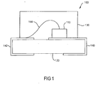
- Figure 1 shows one typical surface mount LED package 100 comprising an LED die 110 mounted on a circuit board substrate 120 with a transparent material 130 encapsulating the LED die 110.
- the package includes a pair of conductive interconnects 140, 142 for coupling the LED to external circuitry.
- a first electrode on the bottom surface of the LED die 110 is mounted on and electrically coupled to one of the pair of conductive interconnects 140.
- a very small wire 144 is then "wire bonded" or welded at one end to a second electrode on the top surface of the LED die 110, and at the other end to the other one of the pair of conductive interconnects 142.
- JP-A07202271 discloses a light source comprising a planar substrate with a recess in which an LED chip is mounted, first and second interconnects extending between the upper and lower surfaces of substrate, and having terminals on the upper surface being coupled to the LED chip as well as pads on the lower surface for coupling to external circuitry.
- a transparent material encapsulating and forming a raised portion over the LED chip is also present.
- the recess has a side wall tapering outwards towards the upper surface of the substrate.
- JP-A08274377 discloses an LED lamp with an elliptic lens of resin material.
- JP-A 06013661 discloses an LED light source for display applications comprising an LED chip with an elliptic lens of resin material.
- the side wall of the recess is plated with a metallic layer presenting a silvered reflective surface to the light emitting diode.
- the silvered reflective surface provides improved reflectivity over previously employed gold layers which present a golden appearance to the light emitting diode.
- the metallic layer forms the terminal of the first interconnect.
- Each of the conductive pads of the first and second interconnects may include a gold plated layer for electrically coupling to external circuitry.
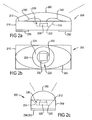
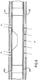
- an LED package 200 which can be surface mounted onto a printed circuit board by, for example, reflow soldering or possibly manual soldering.
- the dimensions of the LED package are preferably 2 millimeters long by 1.25 millimeters wide by 1.2 millimeters tall.
- the light emitting element of the LED package 200 is provided by a light emitting diode (LED) die 230 which is mounted centrally in the recess 220 of the substrate 210.
- LED light emitting diode
- two thin gold wires 240, 242 are electrically coupled at one end to the LED die 230 in order to supply an electric current across a semiconductor junction of the LED die.
- the other ends of the gold wires 240, 242 are electrically coupled to respective terminals on the upper surface 212 of the substrate 210.
- a transparent or translucent encapsulant material 260 is bonded to the upper surface 212 of the substrate 210 so as to encapsulate the terminals on the upper surface 212, the gold wires 240, 242, and the LED die 230.
- the encapsulant material is shaped to form a focussing ellipsoidal dome over the light emitting diode.
- the ellipsoidal shape of the encapsulation dome optimises the surface mount LED package for use in video matrix displays.
- the major axis radius of curvature of the ellipse shown in the front view is relatively large so as to provide a wide viewing angle of approximately 120 degrees. Such a wide viewing angle would be ideally configured in the horizontal plane as is well known in the field of video displays.
- the manufacturing process is actually designed to manufacture multiple surface mount LED packages in one batch.
- the starting material for the manufacturing process is a large glass-fibre laminate board which is divided into an array or grid of identical rectangular units.
- a board may, for example, be an FR4 type substrate with a glass transition phase of 180 degrees centigrade.
- the board has an array of units 40 units wide by 20 units long, and has dimensions of approximately 70 millimeters by 70 millimeters by 0.4 millimeters.
- Each rectangular unit on the board forms the basis of the rectangular substrate 210 of the LED package in Figure 2.
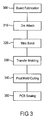
- the same processing steps 300, 310, 320, 330, and 340 are applied to each rectangular unit prior to physical separation of the individual units in the sawing step 350.
- the processing of multiple units on a large board enables the units to be handled more accurately.
- the processing steps will be explained with reference to a single rectangular unit on the board. However, it is understood that the steps will apply to all units on the board
- the first step 300 in the manufacturing process involves preparing the units of the board for the die attach step 310.
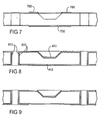
- the board fabrication step 300 is illustrated sequentially in Figures 4 to 14.
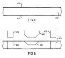
- the bare glass-fiber board unit 400 is first plated on the upper and lower surfaces with copper 410 using standard plating techniques.
- each rectangular unit 400 on the board is drilled with two differently shaped drill bits 430, 450 as illustrated in Figure 5.
- two holes 420, 425 at opposite corners of the rectangular unit are drilled using a first cylindrically shaped drill bit 430.
- These via-like holes 420, 425 extend between the upper and lower surfaces of the board and through the copper plating 410.
- a conical-section shaped recess 440 is drilled in the upper surface of the board centrally on the rectangular unit by a second cylindrically shaped drill bit 450 having a tapered or chamfered end.
- the drill bits remove the copper plating 410 in the drilling areas, leaving surfaces of the board exposed in the two holes 420, 425 and in the recess 440. These exposed areas are then coated with a film of graphite such that the whole surface of the unit becomes electrically conductive.
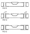
- the drilled unit is subjected to a series of photochemical etching processes which selectively deposit metallic layers in predetermined regions on the unit surface.
- the first photochemical etching processes is illustrated in Figure 6.
- the photochemical etching process comprises applying a dry film 600 made from photosensitive resistive material on the upper and lower surfaces of the unit 400. Photomasks 610, 620 are then applied above and below the upper and lower dry films 600 respectively.
- the photomasks 610, 620 shown respectively in plan in Figures 21 and 22, are generally transparent except for opaque regions which define where a metallic layer should be deposited.
- Figure 8 illustrates the result of electrolytically plating the unit with copper 800 and nickel 810. Because the mask is electrically insulating, no plating occurs over the mask region. In contrast, the remainder of the unit is electrically conductive (including the holes and the recess) and so plating occurs everywhere except the mask region.
- the plated areas define a pair of interconnections on the upper and lower surface of the unit 400 for the LED die.
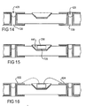
- a second photochemical etching process is then applied to the unit 400 on the upper surface only.
- a dry film 605 made of photosensitive resistive material is applied to the upper surface of the unit 400.
- a photomask 614 shown in plan in Figure 23, is then applied over the dry film and the upper surface of the unit 400 is exposed to UV light.
- the photomask exposes only the recess area to UV light such that the dry film hardens over the recess, and remains in place while the obscured regions are dissolved away by means of a suitable etchant.
- Figure 11 shows the result of this photomasking.
- the last stage in the board fabrication step 300 is to seal the holes 420, 425 with a thermosetting polymer such as a solder resist.
- a thermosetting polymer such as a solder resist.
- the next step 310 in the manufacturing process is to mount or attach an LED die 230 in the recess 440.
- the first stage of this die attach step involves dispensing or dotting a small amount of electrically conductive silver epoxy 720 on the floor or base of the recess.
- the next stage involves picking and placing an LED die 230 onto the silver epoxy in the recess as shown in Figure 15.
- the final stage of the die attach step involves curing the silver epoxy together with the rest of the unit 400 in a box oven at approximately 180 degree centigrade for a period of approximately one hour. The cured silver epoxy fixes the die in place in the recess and provides good heat conductivity away from the die.
- a wire bonding step 320 is employed in the present embodiment to electrically couple the two sides of the semiconductor junction of the LED die to two electrically isolated terminals on the upper side of the unit board.
- the two terminals are provided by the gold plated layers 822, 824 at opposite ends of the unit board.
- the wire bonding process creates a ball joint between one end of gold wire and a bond pad on the LED die, and a wedge joint between the other end of the wire and the gold plated terminal on the unit board.
- a suitable apparatus and method for forming such a wire bond is described in U.S. patent number 4,600,138 .
- the resulting wire bonded LED die is illustrated in Figure 16.
- the batch processing of multiple units is completed in the transfer mold step 330 in which an epoxy encapsulant is molded using a known transfer molding process over the upper surface of the unit 400.
- the mold is of comparable length and width to the original glass fibre board and comprises an array of ellipsoidal mold cups to compliment the array of units on the board.
- the mold process includes a first step of clamping the mold onto the upper surface of the board such that the array of mold cups are positioned to compliment the array of units on the board.
- the second step is to "transfer" a molding compound into the mold cups under elevated temperature and pressure conditions.
- the molding compound could be an MG18 epoxy, available from Dexter Hysol, USA, which is heated to approximately 155 degrees centigrade and is transferred into the mold under a pressure of 1500 kilo Pascals.
- Individual LED packages are produced in the final sawing step in which of individual units on the board array are sawn apart.
- a 0.2 millimeter dicing saw available from Disco Abrasive Systems Inc., Mountain View, California, is used to separate the units.
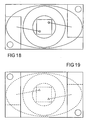
- Detail views of the final surface mount LED package are shown in Figures 17, 18 and 19.
- the invention may be practiced otherwise than as specifically described.
- the nickel plating on the recess which presents a silvered surface to the LED die could be replaced with silver plating to form a silvered surface.
Claims (4)
- Source de lumière (200) comprenant :a) un substrat plan rectangulaire (210, 400) ayant une surface supérieure (212) et une surface inférieure, une partie de la surface supérieure définissant un renfoncement (220, 440) ayant une paroi latérale réfléchissant la lumière (224),b) une matrice de diode électroluminescente (230) montée dans le renfoncement du substrat de manière adjacente à la paroi latérale, etc) un matériau encapsulant transparent (260) relié à la surface supérieure du substrat afin d'encapsuler la matrice de diode électroluminescente, le matériau formant un dôme par-dessus la matrice de diode électroluminescente,
dans laquelle le renfoncement est un renfoncement en forme de section conique positionné de manière centrale sur la surface supérieure, la paroi latérale du renfoncement s'effilant de manière concentrique vers l'extérieur entre un plancher circulaire (222) et un bord circulaire (226) sur la surface supérieure du substrat, et le dôme étant un dôme ellipsoïdal moulé et ayant un axe majeur sensiblement égal à la longueur du substrat et un axe mineur sensiblement égal à la largeur du substrat,
et comprenant en outre :d) une première interconnexion électriquement conductrice s'étendant entre les surfaces supérieure et inférieure, la première interconnexion ayant une borne (822) sur la surface supérieure électriquement couplée à la matrice de diode électroluminescente et une plage exposée (250) sur la surface inférieure, en vue d'un couplage électrique avec des circuits externes, ete) une seconde interconnexion électriquement conductrice s'étendant entre les surfaces supérieure et inférieure, la seconde interconnexion ayant une borne (824) sur la surface supérieure électriquement couplée à la matrice de diode électroluminescente et une plage exposée (252) sur la surface inférieure, en vue d'un couplage électrique avec des circuits externes,dans laquelle le substrat définit un premier et un second trous d'interconnexion (420, 425) s'étendant entre les surfaces supérieure et inférieure, une partie de chacune des première et seconde interconnexions s'étendant dans le premier et le second trous d'interconnexion, respectivement, et dans laquelle les trous d'interconnexion ne sont pas recouverts par le dôme ellipsoïdal. - Source de lumière selon la revendication 1, dans laquelle la paroi latérale du renfoncement est recouverte d'une couche métallique présentant une surface réfléchissante argentée à la matrice de diode électroluminescente.
- Source de lumière selon la revendication 2, dans laquelle la couche métallique forme la borne de la première interconnexion.
- Source de lumière selon l'une quelconque des revendications 1 à 3, dans laquelle chacune des plages conductrices de la première et de la seconde interconnexions comprend une couche recouverte d'or destinée à un couplage électrique avec des circuits externes.
Applications Claiming Priority (2)
| Application Number | Priority Date | Filing Date | Title |
|---|---|---|---|
| MYPI20002918 | 2000-06-28 | ||
| MY0002918 | 2000-06-28 |
Publications (3)
| Publication Number | Publication Date |
|---|---|
| EP1168461A2 EP1168461A2 (fr) | 2002-01-02 |
| EP1168461A3 EP1168461A3 (fr) | 2003-01-22 |
| EP1168461B1 true EP1168461B1 (fr) | 2007-09-19 |
Family
ID=19749463
Family Applications (1)
| Application Number | Title | Priority Date | Filing Date |
|---|---|---|---|
| EP01305515A Expired - Lifetime EP1168461B1 (fr) | 2000-06-28 | 2001-06-26 | Source de lumière |
Country Status (4)
| Country | Link |
|---|---|
| US (1) | US6806583B2 (fr) |
| EP (1) | EP1168461B1 (fr) |
| JP (1) | JP4926337B2 (fr) |
| DE (1) | DE60130520T2 (fr) |
Families Citing this family (44)
| Publication number | Priority date | Publication date | Assignee | Title |
|---|---|---|---|---|
| US20030102527A1 (en) * | 1997-12-31 | 2003-06-05 | Bily Wang | Method of fabricating light emitting diode package |
| US7268479B2 (en) * | 2001-02-15 | 2007-09-11 | Integral Technologies, Inc. | Low cost lighting circuits manufactured from conductive loaded resin-based materials |
| DE10142654A1 (de) * | 2001-08-31 | 2003-04-03 | Osram Opto Semiconductors Gmbh | Sicherungsbauelement mit optischer Anzeige |
| US6906403B2 (en) * | 2002-06-04 | 2005-06-14 | Micron Technology, Inc. | Sealed electronic device packages with transparent coverings |
| DE10246786A1 (de) * | 2002-10-08 | 2004-04-22 | Ultrastar Limited | Gehäusekonstruktion einer LED für Oberflächenmontage sowie Verfahren zum Herstellen derselben |
| ITMI20022467A1 (it) * | 2002-11-20 | 2004-05-21 | St Microelectronics Srl | Processo per realizzare un transistore di selezione di byte per |
| TW560697U (en) * | 2002-11-26 | 2003-11-01 | Topson Technology Co Ltd | Surface-mounting type light-emitting diode structure |
| JP4281363B2 (ja) * | 2003-01-20 | 2009-06-17 | パナソニック電工株式会社 | 配線板及び発光装置 |
| US7734168B2 (en) * | 2003-01-21 | 2010-06-08 | Fujifilm Corporation | Lighting apparatus, electronic flash apparatus and camera |
| JP3948417B2 (ja) * | 2003-02-28 | 2007-07-25 | ノーリツ鋼機株式会社 | 光源ユニット |
| US20040173808A1 (en) * | 2003-03-07 | 2004-09-09 | Bor-Jen Wu | Flip-chip like light emitting device package |
| US7220020B2 (en) * | 2003-05-06 | 2007-05-22 | Ji-Mei Tsuei | Light source device |
| US6995402B2 (en) * | 2003-10-03 | 2006-02-07 | Lumileds Lighting, U.S., Llc | Integrated reflector cup for a light emitting device mount |
| KR100604602B1 (ko) | 2004-05-19 | 2006-07-24 | 서울반도체 주식회사 | 발광 다이오드 렌즈 및 그것을 갖는 발광 다이오드 |
| JP2006093672A (ja) * | 2004-08-26 | 2006-04-06 | Toshiba Corp | 半導体発光装置 |
| US7405433B2 (en) * | 2005-02-22 | 2008-07-29 | Avago Technologies Ecbu Ip Pte Ltd | Semiconductor light emitting device |
| WO2006106901A1 (fr) * | 2005-04-01 | 2006-10-12 | Matsushita Electric Industrial Co., Ltd. | Composant de led et son procede de fabrication |
| CA2617314A1 (fr) * | 2005-04-05 | 2006-10-12 | Tir Technology Lp | Ensemble de montage pour des dispositifs optoelectroniques |
| KR100691174B1 (ko) | 2005-05-24 | 2007-03-09 | 삼성전기주식회사 | 측면형 발광 다이오드 및 그 제조방법 |
| US7105863B1 (en) | 2005-06-03 | 2006-09-12 | Avago Technologies Ecbu Ip (Singapore) Pte. Ltd. | Light source with improved life |
| JP2007088155A (ja) * | 2005-09-21 | 2007-04-05 | Stanley Electric Co Ltd | 表面実装型led基板 |
| EP1949770B1 (fr) * | 2005-11-09 | 2018-12-12 | Koninklijke Philips N.V. | Procede pour produire un support de boitier destine a renfermer au moins un element microelectronique, et procede pour produire un dispositif de diagnostic |
| US8044412B2 (en) | 2006-01-20 | 2011-10-25 | Taiwan Semiconductor Manufacturing Company, Ltd | Package for a light emitting element |
| JP4654942B2 (ja) * | 2006-02-28 | 2011-03-23 | ミネベア株式会社 | 面状照明装置 |
| KR20080032882A (ko) * | 2006-10-11 | 2008-04-16 | 삼성전기주식회사 | 발광 다이오드 패키지 |
| US20080246397A1 (en) * | 2007-04-04 | 2008-10-09 | Bily Wang | Manufacturing method of white light led and structure thereof |
| DE102007043401A1 (de) * | 2007-09-12 | 2009-03-19 | Osram Gesellschaft mit beschränkter Haftung | Leuchtvorrichtung und Verfahren zur Herstellung derselben |
| US8946987B2 (en) | 2007-11-07 | 2015-02-03 | Industrial Technology Research Institute | Light emitting device and fabricating method thereof |
| TWI401820B (zh) * | 2007-11-07 | 2013-07-11 | Ind Tech Res Inst | 發光元件及其製作方法 |
| GB2458345B (en) * | 2008-03-12 | 2012-05-23 | Dialight Lumidrives Ltd | Method and apparatus for providing illumination |
| US8598602B2 (en) | 2009-01-12 | 2013-12-03 | Cree, Inc. | Light emitting device packages with improved heat transfer |
| US7923739B2 (en) | 2009-06-05 | 2011-04-12 | Cree, Inc. | Solid state lighting device |
| US8309973B2 (en) * | 2009-02-12 | 2012-11-13 | Taiwan Semiconductor Manufacturing Company, Ltd. | Silicon-based sub-mount for an opto-electronic device |
| US9111778B2 (en) | 2009-06-05 | 2015-08-18 | Cree, Inc. | Light emitting diode (LED) devices, systems, and methods |
| US8860043B2 (en) * | 2009-06-05 | 2014-10-14 | Cree, Inc. | Light emitting device packages, systems and methods |
| JP5612355B2 (ja) * | 2009-07-15 | 2014-10-22 | 株式会社Kanzacc | メッキ構造及び電気材料の製造方法 |
| US8101962B2 (en) * | 2009-10-06 | 2012-01-24 | Kuang Hong Precision Co., Ltd. | Carrying structure of semiconductor |
| CN102237466B (zh) * | 2010-04-28 | 2013-11-06 | 展晶科技(深圳)有限公司 | 发光组件封装结构及其制程 |
| EP2390909A1 (fr) * | 2010-05-24 | 2011-11-30 | Jerry Hu | Mise en boîtier miniature pour des composants discrets |
| US8269244B2 (en) | 2010-06-28 | 2012-09-18 | Cree, Inc. | LED package with efficient, isolated thermal path |
| US11101408B2 (en) | 2011-02-07 | 2021-08-24 | Creeled, Inc. | Components and methods for light emitting diode (LED) lighting |
| TW201251140A (en) | 2011-01-31 | 2012-12-16 | Cree Inc | High brightness light emitting diode (LED) packages, systems and methods with improved resin filling and high adhesion |
| JP2014063967A (ja) * | 2012-09-24 | 2014-04-10 | Towa Corp | 発光デバイス及びその製造方法、並びに発光デバイス成形用金型 |
| KR101912290B1 (ko) * | 2017-12-06 | 2018-10-29 | 삼성전기 주식회사 | 팬-아웃 반도체 패키지 |
Citations (3)
| Publication number | Priority date | Publication date | Assignee | Title |
|---|---|---|---|---|
| JPH0613661A (ja) * | 1992-06-25 | 1994-01-21 | Rohm Co Ltd | 発光ダイオード |
| JPH06177428A (ja) * | 1992-12-03 | 1994-06-24 | Rohm Co Ltd | 発光ダイオードランプ |
| JPH1187780A (ja) * | 1997-09-04 | 1999-03-30 | Sharp Corp | 発光装置 |
Family Cites Families (26)
| Publication number | Priority date | Publication date | Assignee | Title |
|---|---|---|---|---|
| DE3128187A1 (de) * | 1981-07-16 | 1983-02-03 | Joachim 8068 Pfaffenhofen Sieg | Opto-elektronisches bauelement |
| JPS61240687A (ja) * | 1985-04-18 | 1986-10-25 | Matsushita Electric Ind Co Ltd | 発光素子 |
| US5278429A (en) * | 1989-12-19 | 1994-01-11 | Fujitsu Limited | Semiconductor device having improved adhesive structure and method of producing same |
| JPH04102378A (ja) * | 1990-08-21 | 1992-04-03 | Sanyo Electric Co Ltd | 発光ダイオード装置の製造方法 |
| US5221641A (en) * | 1991-06-21 | 1993-06-22 | Rohm Co., Ltd. | Process for making light emitting diodes |
| DE4242842C2 (de) * | 1992-02-14 | 1999-11-04 | Sharp Kk | Lichtemittierendes Bauelement zur Oberflächenmontage und Verfahren zu dessen Herstellung |
| JP3227295B2 (ja) * | 1993-12-28 | 2001-11-12 | 松下電工株式会社 | 発光ダイオードの製造方法 |
| JPH07209764A (ja) * | 1994-01-18 | 1995-08-11 | Nikon Corp | 光源装置 |
| JP3137823B2 (ja) * | 1994-02-25 | 2001-02-26 | シャープ株式会社 | チップ部品型led及びその製造方法 |
| KR100309623B1 (ko) * | 1994-02-28 | 2002-04-24 | 사토 게니치로 | 발광다이오드램프및이를이용한매트릭스표시기 |
| JP3579944B2 (ja) | 1995-01-27 | 2004-10-20 | ソニー株式会社 | 表示装置 |
| JP2927202B2 (ja) * | 1995-03-29 | 1999-07-28 | 日亜化学工業株式会社 | Ledランプ |
| DE19549818B4 (de) * | 1995-09-29 | 2010-03-18 | Osram Opto Semiconductors Gmbh | Optoelektronisches Halbleiter-Bauelement |
| US5786626A (en) * | 1996-03-25 | 1998-07-28 | Ibm Corporation | Thin radio frequency transponder with leadframe antenna structure |
| US6045240A (en) * | 1996-06-27 | 2000-04-04 | Relume Corporation | LED lamp assembly with means to conduct heat away from the LEDS |
| US5777433A (en) * | 1996-07-11 | 1998-07-07 | Hewlett-Packard Company | High refractive index package material and a light emitting device encapsulated with such material |
| TW383508B (en) * | 1996-07-29 | 2000-03-01 | Nichia Kagaku Kogyo Kk | Light emitting device and display |
| US6054716A (en) * | 1997-01-10 | 2000-04-25 | Rohm Co., Ltd. | Semiconductor light emitting device having a protecting device |
| KR100266071B1 (ko) * | 1997-07-03 | 2000-09-15 | 윤종용 | 칩 온 보드 패키지용 인쇄회로기판 및 그를 이용한 칩 온 보드 패키지 |
| JP3432113B2 (ja) * | 1997-07-07 | 2003-08-04 | シャープ株式会社 | 光半導体装置 |
| TW414924B (en) * | 1998-05-29 | 2000-12-11 | Rohm Co Ltd | Semiconductor device of resin package |
| DE19829197C2 (de) * | 1998-06-30 | 2002-06-20 | Siemens Ag | Strahlungsaussendendes und/oder -empfangendes Bauelement |
| US5959316A (en) * | 1998-09-01 | 1999-09-28 | Hewlett-Packard Company | Multiple encapsulation of phosphor-LED devices |
| JP2000223751A (ja) * | 1998-11-25 | 2000-08-11 | Nichia Chem Ind Ltd | Ledランプ及びそれを用いた表示装置 |
| JP2000183407A (ja) * | 1998-12-16 | 2000-06-30 | Rohm Co Ltd | 光半導体装置 |
| US6407411B1 (en) * | 2000-04-13 | 2002-06-18 | General Electric Company | Led lead frame assembly |
-
2001
- 2001-06-21 JP JP2001188140A patent/JP4926337B2/ja not_active Expired - Fee Related
- 2001-06-25 US US09/888,857 patent/US6806583B2/en not_active Expired - Lifetime
- 2001-06-26 EP EP01305515A patent/EP1168461B1/fr not_active Expired - Lifetime
- 2001-06-26 DE DE60130520T patent/DE60130520T2/de not_active Expired - Lifetime
Patent Citations (3)
| Publication number | Priority date | Publication date | Assignee | Title |
|---|---|---|---|---|
| JPH0613661A (ja) * | 1992-06-25 | 1994-01-21 | Rohm Co Ltd | 発光ダイオード |
| JPH06177428A (ja) * | 1992-12-03 | 1994-06-24 | Rohm Co Ltd | 発光ダイオードランプ |
| JPH1187780A (ja) * | 1997-09-04 | 1999-03-30 | Sharp Corp | 発光装置 |
Also Published As
| Publication number | Publication date |
|---|---|
| US6806583B2 (en) | 2004-10-19 |
| JP4926337B2 (ja) | 2012-05-09 |
| DE60130520D1 (de) | 2007-10-31 |
| DE60130520T2 (de) | 2008-06-26 |
| EP1168461A3 (fr) | 2003-01-22 |
| US20020047130A1 (en) | 2002-04-25 |
| JP2002064226A (ja) | 2002-02-28 |
| EP1168461A2 (fr) | 2002-01-02 |
Similar Documents
| Publication | Publication Date | Title |
|---|---|---|
| EP1168461B1 (fr) | Source de lumière | |
| US6949771B2 (en) | Light source | |
| US6730533B2 (en) | Plastic packaging of LED arrays | |
| TWI382561B (zh) | 附有反射透鏡之功率發光二極體封裝及其製造方法 | |
| US6531328B1 (en) | Packaging of light-emitting diode | |
| JP5520243B2 (ja) | 電力表面取り付けの発光ダイ・パッケージ | |
| CN102148316B (zh) | 采用电表面安装的发光晶片封装 | |
| US8153477B2 (en) | Method of making a semiconductor chip assembly with a post/dielectric/post heat spreader | |
| US6696310B2 (en) | Manufacturing method of lighting device | |
| US20060261450A1 (en) | Leadframeless package structure and method | |
| CN102549785B (zh) | 发光装置 | |
| JP2009117536A (ja) | 樹脂封止発光体及びその製造方法 | |
| CN103748700A (zh) | 用于led封装的带有凹坑和通孔的基板 | |
| CN102983256A (zh) | 发光二极管封装 | |
| CN102983125B (zh) | Led封装、其制作方法及包含其的led系统 | |
| US8415703B2 (en) | Semiconductor chip assembly with post/base/flange heat spreader and cavity in flange | |
| JPH1050734A (ja) | チップ型半導体 | |
| CN116613267A (zh) | 一种微型led发光器件扇出封装结构及制备方法 | |
| KR100808644B1 (ko) | 표면 실장형 발광 다이오드 램프 및 그 제조 방법 | |
| JP2001068740A (ja) | 電子デバイスを相互接続するための方法 | |
| EP1676471B1 (fr) | Dispositif electronique et son procede de fabrication | |
| KR101824177B1 (ko) | 리드프레임을 이용한 반도체 패키지 및 그 제조 방법 | |
| JP2002026180A (ja) | 回路装置の製造方法 |
Legal Events
| Date | Code | Title | Description |
|---|---|---|---|
| PUAI | Public reference made under article 153(3) epc to a published international application that has entered the european phase |
Free format text: ORIGINAL CODE: 0009012 |
|
| AK | Designated contracting states |
Kind code of ref document: A2 Designated state(s): AT BE CH CY DE DK ES FI FR GB GR IE IT LI LU MC NL PT SE TR |
|
| AX | Request for extension of the european patent |
Free format text: AL;LT;LV;MK;RO;SI |
|
| RIN1 | Information on inventor provided before grant (corrected) |
Inventor name: NATARAJAN YOGANANDAN, SUNDAR A/L Inventor name: SINGH, GURBIR Inventor name: CHONG, CHEE KEONG Inventor name: LIM, SEONG CHOON Inventor name: TAN, CHENG WHY Inventor name: KOAY, HUCK KHIM |
|
| RIN1 | Information on inventor provided before grant (corrected) |
Inventor name: CHONG, CHEE KEONG Inventor name: KOAY, HUCK KHIM Inventor name: TAN, CHENG WHY Inventor name: SINGH, GURBIR Inventor name: LIM, SEONG CHOON Inventor name: NATARAJAN YOGANANDAN, SUNDAR A/L |
|
| PUAL | Search report despatched |
Free format text: ORIGINAL CODE: 0009013 |
|
| AK | Designated contracting states |
Kind code of ref document: A3 Designated state(s): AT BE CH CY DE DK ES FI FR GB GR IE IT LI LU MC NL PT SE TR |
|
| AX | Request for extension of the european patent |
Free format text: AL;LT;LV;MK;RO;SI |
|
| 17P | Request for examination filed |
Effective date: 20030610 |
|
| AKX | Designation fees paid |
Designated state(s): DE ES FR GB |
|
| 17Q | First examination report despatched |
Effective date: 20030904 |
|
| RAP1 | Party data changed (applicant data changed or rights of an application transferred) |
Owner name: AVAGO TECHNOLOGIES GENERAL IP (SINGAPORE) PTE. LTD |
|
| GRAP | Despatch of communication of intention to grant a patent |
Free format text: ORIGINAL CODE: EPIDOSNIGR1 |
|
| GRAS | Grant fee paid |
Free format text: ORIGINAL CODE: EPIDOSNIGR3 |
|
| GRAA | (expected) grant |
Free format text: ORIGINAL CODE: 0009210 |
|
| AK | Designated contracting states |
Kind code of ref document: B1 Designated state(s): DE ES FR GB |
|
| REG | Reference to a national code |
Ref country code: GB Ref legal event code: FG4D |
|
| REF | Corresponds to: |
Ref document number: 60130520 Country of ref document: DE Date of ref document: 20071031 Kind code of ref document: P |
|
| PG25 | Lapsed in a contracting state [announced via postgrant information from national office to epo] |
Ref country code: ES Free format text: LAPSE BECAUSE OF FAILURE TO SUBMIT A TRANSLATION OF THE DESCRIPTION OR TO PAY THE FEE WITHIN THE PRESCRIBED TIME-LIMIT Effective date: 20071230 |
|
| EN | Fr: translation not filed | ||
| PLBE | No opposition filed within time limit |
Free format text: ORIGINAL CODE: 0009261 |
|
| STAA | Information on the status of an ep patent application or granted ep patent |
Free format text: STATUS: NO OPPOSITION FILED WITHIN TIME LIMIT |
|
| 26N | No opposition filed |
Effective date: 20080620 |
|
| PG25 | Lapsed in a contracting state [announced via postgrant information from national office to epo] |
Ref country code: FR Free format text: LAPSE BECAUSE OF FAILURE TO SUBMIT A TRANSLATION OF THE DESCRIPTION OR TO PAY THE FEE WITHIN THE PRESCRIBED TIME-LIMIT Effective date: 20080523 |
|
| REG | Reference to a national code |
Ref country code: GB Ref legal event code: 732E Free format text: REGISTERED BETWEEN 20130207 AND 20130214 |
|
| REG | Reference to a national code |
Ref country code: DE Ref legal event code: R082 Ref document number: 60130520 Country of ref document: DE Representative=s name: DILG HAEUSLER SCHINDELMANN PATENTANWALTSGESELL, DE Effective date: 20130227 Ref country code: DE Ref legal event code: R081 Ref document number: 60130520 Country of ref document: DE Owner name: INTELLECTUAL DISCOVERY CO., LTD., KR Free format text: FORMER OWNER: AVAGO TECHNOLOGIES GENERAL IP (SINGAPORE) PTE. LTD., SINGAPUR/SINGAPORE, SG Effective date: 20130227 Ref country code: DE Ref legal event code: R081 Ref document number: 60130520 Country of ref document: DE Owner name: INTELLECTUAL DISCOVERY CO., LTD., KR Free format text: FORMER OWNER: AVAGO TECHNOLOGIES GENERAL IP (SINGAPORE) PTE. LTD., SINGAPORE, SG Effective date: 20130227 |
|
| PGFP | Annual fee paid to national office [announced via postgrant information from national office to epo] |
Ref country code: DE Payment date: 20180627 Year of fee payment: 18 Ref country code: GB Payment date: 20180627 Year of fee payment: 18 |
|
| REG | Reference to a national code |
Ref country code: DE Ref legal event code: R119 Ref document number: 60130520 Country of ref document: DE |
|
| GBPC | Gb: european patent ceased through non-payment of renewal fee |
Effective date: 20190626 |
|
| PG25 | Lapsed in a contracting state [announced via postgrant information from national office to epo] |
Ref country code: DE Free format text: LAPSE BECAUSE OF NON-PAYMENT OF DUE FEES Effective date: 20200101 Ref country code: GB Free format text: LAPSE BECAUSE OF NON-PAYMENT OF DUE FEES Effective date: 20190626 |