EP1168181A2 - IC, IC-mounted electronic device, debugging method and IC debugger - Google Patents
IC, IC-mounted electronic device, debugging method and IC debugger Download PDFInfo
- Publication number
- EP1168181A2 EP1168181A2 EP01401743A EP01401743A EP1168181A2 EP 1168181 A2 EP1168181 A2 EP 1168181A2 EP 01401743 A EP01401743 A EP 01401743A EP 01401743 A EP01401743 A EP 01401743A EP 1168181 A2 EP1168181 A2 EP 1168181A2
- Authority
- EP
- European Patent Office
- Prior art keywords
- circuit
- debug
- authentication
- key
- transmission key
- Prior art date
- Legal status (The legal status is an assumption and is not a legal conclusion. Google has not performed a legal analysis and makes no representation as to the accuracy of the status listed.)
- Withdrawn
Links
Images





Classifications
-
- G—PHYSICS
- G06—COMPUTING OR CALCULATING; COUNTING
- G06F—ELECTRIC DIGITAL DATA PROCESSING
- G06F11/00—Error detection; Error correction; Monitoring
- G06F11/36—Prevention of errors by analysis, debugging or testing of software
- G06F11/362—Debugging of software
- G06F11/3648—Debugging of software using additional hardware
- G06F11/3656—Debugging of software using additional hardware using a specific debug interface
-
- G—PHYSICS
- G01—MEASURING; TESTING
- G01R—MEASURING ELECTRIC VARIABLES; MEASURING MAGNETIC VARIABLES
- G01R31/00—Arrangements for testing electric properties; Arrangements for locating electric faults; Arrangements for electrical testing characterised by what is being tested not provided for elsewhere
- G01R31/28—Testing of electronic circuits, e.g. by signal tracer
- G01R31/317—Testing of digital circuits
- G01R31/31719—Security aspects, e.g. preventing unauthorised access during test
Definitions
- the present invention relates to an IC, an electronic device, a method for debugging the IC, a method for debugging the electronic device, and a debugger, having a security function for preventing a spurious acquisition of a behavior of an internal circuit of the IC.
- Fig. 9 is an explanatory diagram of the prior art.
- an LSI 110 is provided with a CPU 200, a peripheral circuit 300, and a bus 600 for connecting therewith.
- the CPU 200 acquires data or programs from the peripheral circuit 300, and processes the data, and outputs them to the peripheral circuit 300.
- the CPU 200 is provided with a debug I/F (interface) circuit 400 via another bus 500.
- An external debug controller 100 of the LSI 110 is connected to the debug I/F 400, and supplies a clock CLK, and inputs a signal SIN, and obtains an output SOUT.
- This debug I/F circuit 400 is exploited for acquiring a behavior (contents of a program counter, a register, or the like) of the CPU 200 at the time of developing the device, and in the case where the device is shipped to a field, the debug I/F circuit 400 is similarly exploited at the time of the occurrence of a fault, and at the time of diagnosing the device.
- a security function is not provided in the prior art with respect to an access from the debug I/F 400, as described above.
- a debug I/F terminal In the device which does not require a conventional normal security, a debug I/F terminal is seen from outside irrespective of the time of being unused/the time of being used, and is entirely defenseless for the exploitation by the third person. For this reason, in the case of the device shipped to the field, the third person uses the debug I/F terminal, so that a behavior of a central processing unit (CPU) can accurately and readily be reverse-engineered, and thus needs high-performance in security.
- CPU central processing unit
- a clue of analysis is given to the third person.
- a debug unit of the debug I/F is connected to a personal computer etc., so that even data such as a password, a cryptographic key, or the like can readily be searched.
- an IC comprising an internal circuit; a debug I/F circuit for debugging the internal circuit from externally; and an authentication circuit which is provided between the debug I/F circuit and a debug terminal, and when the debug I/F circuit is activated, transmits a transmission key from the debug terminal to outside, and authenticates from a signal received from the debug terminal and a transmission key, and enables operation of the debug I/F circuit.
- an electronic device mounted with an IC comprising an internal circuit; a debug I/F circuit for debugging the internal circuit from externally; and an authentication circuit which is provided between the debug I/F circuit and the debug terminal, and when the debug I/F circuit is activated, transmits the transmission key from the debug terminal to outside, and collates the signal received from the debug terminal with the transmission key, and enables operation of the debug I/F circuit.
- a debugging method comprising the steps of transmitting the transmission key to externally when the debug I/F circuit is activated; and authenticating the signal received from externally and the transmission key to enable operation of the debug I/F circuit.
- a debugger for debugging an IC comprising an internal circuit; a debug I/F circuit for externally debugging the internal circuit; and an authentication circuit which is provided between the debug I/F circuit and the debug terminal, and when the debug I/F circuit is activated, transmits the transmission key from the debug terminal to outside, and collates the signal received from the debug terminal with the transmission key, and enables operation of the debug I/F circuit, further comprising: the discrimination device which is provided between a debug unit and the debug I/F circuit, and receives the transmission key to encode it by a predetermined key, and transmits the reception signal.
- an authentication circuit is provided between the debug I/F circuit and the debug terminal, it is possible to protect an internal circuit from a dishonesty such as performing reverse engineering of a motion of the internal circuit, etc. by exploiting the debug I/F of the third person, and to hold security higher than a conventional device.
- the authentication step has a step of canceling a reset signal to the debug I/F circuit for enabling of the operation.
- the authentication circuit cancels the reset signal to the debug I/F circuit for enabling of the operation. For this reason, even if authenticated, it is possible to realize by cancellation of the existent reset.
- the authentication circuit forms an authentication key by encoding the transmission key by a predetermined key, and compares the reception signal with the authentication key.
- the authentication step has a step of forming the authentication key by encoding the transmission key by the predetermined key, and of collating the reception signal with the authentication key. Thanks to this encoding, a higher security is possible.
- the authentication circuit awaits a time of the operation enabling.
- the authentication step has a step of waiting a time of the operation enabling. Before and after judgment of a serial data key, a waiting time is provided after the end of agreement judgment by use of a timer. For this reason, even if the third person inputs any cryptographic key data, it takes much time to obtain authentication results (reset). This causes to prevent the use of the spurious debug I/F by the third person, and furthermore when retrying several times, it takes enormous time.
- the authentication circuit forms the transmission key with random numbers, whereby each time serial data (transmission key) to be transmitted are activated, the random numbers are based, so that the serial data are set as transmission and reception data different every time, rendering the analysis thereof difficult.
- Fig. 1 is a block diagram of an LSI and a debug mechanism according to a first embodiment of the present invention
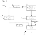
- Fig. 2 is an explanatory diagram of the authentication processing
- Fig. 3 is a diagram for explaining operation at the time of a due use
- Fig. 4 is a diagram for explaining operation at the time of a spurious use.
- reference numeral 2 denotes a system LSI with a CPU.
- a debug I/F utilization authentication circuit according to the present invention is provided to the LSI 2.
- Reference numeral 1 denotes an external debug controller for utilizing the debug I/F inside the LSI 2.
- Reference numeral 3 denotes a discrimination device, which is interposed between the LSI 2 and the debug controller 1, so as to interlock with the authentication circuit inside the LSI 2 and authenticate.
- the LSI 2 has a debug I/F circuit 2-1, a CPU 2-2, a debug bus 4-1 for connecting the I/F circuit 2-1 and the CPU 2-2, and a peripheral circuit 2-12 connected to a CPU bus 4-2.
- the peripheral circuit 2-12 is different according to the use of LSIs, for example, an electronic money funds transferring circuit that will be explained in Fig. 6.
- the authentication circuit is provided in this CPU bus 4-2. A structure of the authentication circuit is explained.
- a port 4-2 receives write data of the CPU 2-2 from the bus 4-2.
- a register 2-5 stores a debug I/F utilization transmission key formed by the CPU 2-2.
- a register 2-8 stores an authentication key formed by the CPU 2-2.
- a transmission circuit 2-4 transmits the transmission key of the register 2-5 in synchronism with a clock supplied by the discrimination device 3.
- a shift register 2-6 receives a cryptographic key returned from the discrimination device 3.
- An agreement detection circuit 2-9 compares a cryptographic key of the shift register 2-6 with an authentication key of a register 2-8, and detects an agreement.
- a timer circuit 2-7 starts counting clocks in response to an agreement detection output of the agreement detection circuit 2-9, and forms a signal for canceling a reset signal to the internal debug I/F circuit 2-1 after a constant time.
- a reset gate 2-11 cancels an input to the debug I/F circuit 2-1 of the reset signal according to a reset cancellation signal.
- a reception-enabling gate 2-10 enables the shift register 2-6 which fetches in data from a signal input terminal SIN in response to a reception-enabling signal from a transmission circuit 2-4.
- the discrimination device 3 is provided with a key reception circuit 3-1.
- the key reception circuit 3-1 transmits clocks and receives the aforesaid transmission key, and encodes it by a key determined previously and transmits the cryptographic key.
- the debug controller 1 utilizing the debug I/F is connected to the LSI 2 via the discrimination device 3.
- the debug I/F circuit 2-1 of the LSI 2 can be utilized. Namely, the reset signal is transmitted from the debug controller 1 to the LSI 2, and resets the debug I/F circuit 2-1, and utilizes the debug I/F circuit 2-1, and can access the CPU 2-2.
- a LSI provider offers the LSI 2 and discrimination device 3 to a developer for an apparatus.
- the encryption key of the LSI 2 is the same as the encryption key of the discrimination device 3.
- the developer mounts the LSI 2 on the target board 7, and develops the device.
- the LSI 2 is connected to the discrimination device 3, which is connected to the debug controller 1, the PC interface board 6, and the personal computer 5.
- the discrimination device 3 intervenes therebetween, the above authentication sequence works to cancel a reset, so that the debugger on the PC 5 can utilize the debug I/F circuit 2-1. Furthermore, even after the device is shipped to a field, the discrimination device 3 is connected, thereby utilizing the debugger on the PC 5.
- a security technique such as a conventional password authentication, etc.
- the security function is not performed, and the password is easy to elucidate by retrying. Accordingly, the security technique is unfit as a security mechanism of the LSI 2 to be presented to a great number of users.
- the security since in order to obtain the security with a set of the discrimination device 3 and LSI 2, the security is carried out by the physical connection and authentication algorithm, a high security is enabled. Furthermore, the spurious engineering by the PC 5 is difficult.
- the aforesaid utilization authentication function is an encryption algorithm
- a skillful spurious person knows existence of the authentication mechanism and tries the engineering by retrying the encryption key (data).
- this engineering becomes difficult, the next technique is adopted.
- the random numbers are based, so that the engineering becomes difficult as set as transmission and reception data different each time.
- the reception operation of the shift register is conducted for a constant time after the transmission key is transmitted, and only one time reception is made at the time of one time activation, and since if data are repeatedly input, not accepted, the engineering is difficult.
- the description device 3 adopts a method of encoding the received transmission key and use ID by the key, thereby preventing the user ID from being readily changed.
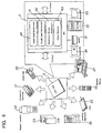
- Fig. 6 is an explanatory diagram of an example to which the system LSI 2 is applied
- Fig. 7 is a structural diagram of a peripheral circuit of the LSI 2 in this application example
- Fig. 8 is an explanatory diagram of the electronic devices.
- the system LSI 2 is a card funds transferring LSI, and has a debit card funds transfer function 40, a credit card funds transfer function 41, an electronic money funds transfer function 42, and other service functions 43.
- the LSI 2 is connected to an IC card reader/writer 30, a magnetic card reader 31, and a display and key 32.
- the LSI 2 is connected to a receipt printer 33.
- These funds transfer functions 40 to 43 are realized by execution of the programs of the CPU 2-2 of the LSI 2.
- a card funds transfer function is imparted to various electronic devices 50 to 57.
- electronic devices are, for example, a POS (point of sales) reader/writer 50, an integrated terminal 51, a mobile terminal 52, an ATM (automatic teller machine) 53, an automatic vending machine 54, a PDA (personal digital assistant) 55, a portable telephone 56, and a PC (personal computer) 57.
- POS point of sales
- PDA personal digital assistant
- peripheral circuit 2-12 of the LSI 2 for the card funds transfer will be explained with reference to Fig. 7.
- the peripheral circuit 2-12 has a smart card controller 60, a MS (Magnetic stripe) control circuit 61, a LCD control circuit 62, a matrix KB control circuit 63, a memory controller 64, and serial I/O ports 69 to 72.
- Fig. 7 shows the above LSI 2 mounted on the target board 7, and for clarity of description of the LSI 2, only the CPU 2-2 and peripheral circuit 2-12 (60-64, 69-72) are shown. Of course, the LSI 2 includes the debug I/F 2-1 and the authentication circuit.
- the smart card controller 60 reads/writes data of the IC card (called a smart card) via the IC card reader/writer 30.
- the MS control circuit controls the MS (magnetic stripe) reader 31.
- the LCD control circuit 62 controls a display of the LCD (liquid crystal display) 32-1.
- the matrix KB control circuit 63 recognizes an input of a ten key 32-2.
- the memory controller 64 controls an input/output into/from various memories (a ROM 65, a SRAM 66, a FLASH 67, a SDRAM 68) on the board 7.
- the serial ports 69 to 72 are connected to drivers 73 to 75 of the port 7 for inputting and outputting the serial data. These are each connected to the CPU bus 4-2.
- Fig. 8 is a system configuration diagram of the electronic device comprising a funds transferring LSI, showing a POS (point of sales) system.
- the network 35 is connected to a store controller 20 and a plurality of POS terminals 10.
- the POS terminals 10 are connected to the IC card reader/writer 30.
- the store controller 20 and the plurality of POS terminals 10 are provided with the above funds transferring LSIs (called an IFD), which exchanges directly funs transfer data.
- IFD funds transferring LSIs
- An IC card 34-1 for customers exchanges messages with a POS IC card 34-2 via the IFD 2
- the POS IC card 34-2 exchanges messages with the IC card 34-2 of the store controller 20 via an IFD 2, a terminal controller 11, a network 35, the terminal controller 11, and the IFD 2.
- customer's data of the IC card 34-1 are stored in the POS IC card 34-2 via the IFD 2.
- the stored data of the POS IC card 34-2 are stored in the IC card 34-2 of the store controller 20 via the IFD 2, the terminal controller 11, the network 35, the terminal controller 11, and the IFD 2.
- an authentication mechanism according to the present invention is, in particular, valid for such uses.
- the authentication circuit is provided between the debug I/F circuit and the debug terminal, it is possible to protect the internal circuit from dishonesty such as the reverse engineering, etc. of operation of the internal circuit by utilizing the debug I/F of the third person, and to hold the security higher than the conventional device.
Landscapes
- Engineering & Computer Science (AREA)
- Computer Hardware Design (AREA)
- Theoretical Computer Science (AREA)
- Quality & Reliability (AREA)
- Physics & Mathematics (AREA)
- General Engineering & Computer Science (AREA)
- General Physics & Mathematics (AREA)
- Storage Device Security (AREA)
- Test And Diagnosis Of Digital Computers (AREA)
- Debugging And Monitoring (AREA)
Abstract
Description
- The present invention relates to an IC, an electronic device, a method for debugging the IC, a method for debugging the electronic device, and a debugger, having a security function for preventing a spurious acquisition of a behavior of an internal circuit of the IC.
- In every field such as an electronic commerce, etc., a device of higher security is demanded. For this reason, various methods for preventing a reverse engineering in the device have been devised. However, irrespective of these trials, a reverse engineering ROM, or the like has been prepared, and an abuse for a reluctant use for a developer of the device does not become extinct. For this reason, a system in which a third person is incapable of engineering operation itself of the device is demanded.
- Fig. 9 is an explanatory diagram of the prior art. As shown in Fig. 9, an
LSI 110 is provided with aCPU 200, aperipheral circuit 300, and abus 600 for connecting therewith. In thisLSI 110, theCPU 200 acquires data or programs from theperipheral circuit 300, and processes the data, and outputs them to theperipheral circuit 300. - On the other hand, in the case where the device is developed by use of this
LSI 110, a processing behavior of theCPU 200 is directly monitored, and the programs or the like are verified. A verification method for monitoring output data of theperipheral circuit 300 is executed, but a behavior of theCPU 200 up to the output cannot be elucidated from the output data. - For this reason, the
CPU 200 is provided with a debug I/F (interface)circuit 400 via anotherbus 500. Anexternal debug controller 100 of theLSI 110 is connected to the debug I/F 400, and supplies a clock CLK, and inputs a signal SIN, and obtains an output SOUT. - This debug I/
F circuit 400 is exploited for acquiring a behavior (contents of a program counter, a register, or the like) of theCPU 200 at the time of developing the device, and in the case where the device is shipped to a field, the debug I/F circuit 400 is similarly exploited at the time of the occurrence of a fault, and at the time of diagnosing the device. - A security function is not provided in the prior art with respect to an access from the debug I/
F 400, as described above. - In the device which does not require a conventional normal security, a debug I/F terminal is seen from outside irrespective of the time of being unused/the time of being used, and is entirely defenseless for the exploitation by the third person. For this reason, in the case of the device shipped to the field, the third person uses the debug I/F terminal, so that a behavior of a central processing unit (CPU) can accurately and readily be reverse-engineered, and thus needs high-performance in security.
- However, in the case where the conventional device uses the CPU provided with the debug I/F function, a clue of analysis is given to the third person. For example, in the case of a POS register using the CPU with the debug I/F function, a debug unit of the debug I/F is connected to a personal computer etc., so that even data such as a password, a cryptographic key, or the like can readily be searched.
- It is therefore an object of the present invention to provide an IC, an electronic device, a debug method, and a debugger for restricting a use of a debug I/F and preventing a spurious reverse engineering by a third person.
- It is another object of the present invention to provide an IC, an electronic device, a debug method, and a debugger in which an authentication logic is provided between the debug I/F circuit in the LSI and an external terminal, and a restriction is formed in exploiting the debug I/F.
- It is yet another object of the present invention to provide an IC, an electronic device, a debug method, and a debugger for preventing the engineering of the authentication logic between the debug I/F circuit in the LSIs and the external terminal.
- It is a further object of the present invention to provide an IC, an electronic device, a debug method, and a debugger for detecting the spurious reverse engineering by a third person which restricts the use of the debug I/F.
- In order to attain the above objects, according to a first aspect of the present invention there is provided an IC comprising an internal circuit; a debug I/F circuit for debugging the internal circuit from externally; and an authentication circuit which is provided between the debug I/F circuit and a debug terminal, and when the debug I/F circuit is activated, transmits a transmission key from the debug terminal to outside, and authenticates from a signal received from the debug terminal and a transmission key, and enables operation of the debug I/F circuit.
- According to a second aspect of the present invention there is provided an electronic device mounted with an IC, the IC comprising an internal circuit; a debug I/F circuit for debugging the internal circuit from externally; and an authentication circuit which is provided between the debug I/F circuit and the debug terminal, and when the debug I/F circuit is activated, transmits the transmission key from the debug terminal to outside, and collates the signal received from the debug terminal with the transmission key, and enables operation of the debug I/F circuit.
- According to a third aspect of the present invention there is provided a debugging method comprising the steps of transmitting the transmission key to externally when the debug I/F circuit is activated; and authenticating the signal received from externally and the transmission key to enable operation of the debug I/F circuit.
- According to a fourth aspect of the present invention there is provided a debugger for debugging an IC, the IC comprising an internal circuit; a debug I/F circuit for externally debugging the internal circuit; and an authentication circuit which is provided between the debug I/F circuit and the debug terminal, and when the debug I/F circuit is activated, transmits the transmission key from the debug terminal to outside, and collates the signal received from the debug terminal with the transmission key, and enables operation of the debug I/F circuit, further comprising: the discrimination device which is provided between a debug unit and the debug I/F circuit, and receives the transmission key to encode it by a predetermined key, and transmits the reception signal.
- Since an authentication circuit is provided between the debug I/F circuit and the debug terminal, it is possible to protect an internal circuit from a dishonesty such as performing reverse engineering of a motion of the internal circuit, etc. by exploiting the debug I/F of the third person, and to hold security higher than a conventional device.
- Furthermore, since the security is performed by a physical connection and an authentication algorithm by a set of a discrimination device and an IC, a high security is enabled. Furthermore, a spurious engineering by a PC (personal computer) is difficult.
- Furthermore, in the debugging method according to the present invention, the authentication step has a step of canceling a reset signal to the debug I/F circuit for enabling of the operation. In the LSI according to the present invention, the authentication circuit cancels the reset signal to the debug I/F circuit for enabling of the operation. For this reason, even if authenticated, it is possible to realize by cancellation of the existent reset.
- Furthermore, in the LSI according to the present invention, the authentication circuit forms an authentication key by encoding the transmission key by a predetermined key, and compares the reception signal with the authentication key. In the debugging method according to the present invention, the authentication step has a step of forming the authentication key by encoding the transmission key by the predetermined key, and of collating the reception signal with the authentication key. Thanks to this encoding, a higher security is possible.
- In the LSI according to the present invention, the authentication circuit awaits a time of the operation enabling. In the debugging method according to the present invention, the authentication step has a step of waiting a time of the operation enabling. Before and after judgment of a serial data key, a waiting time is provided after the end of agreement judgment by use of a timer. For this reason, even if the third person inputs any cryptographic key data, it takes much time to obtain authentication results (reset). This causes to prevent the use of the spurious debug I/F by the third person, and furthermore when retrying several times, it takes enormous time.
- In the LSI according to the present invention, the authentication circuit forms the transmission key with random numbers, whereby each time serial data (transmission key) to be transmitted are activated, the random numbers are based, so that the serial data are set as transmission and reception data different every time, rendering the analysis thereof difficult.
-
- Fig. 1 is a block diagram of an LSI according to an embodiment of the present invention;
- Fig. 2 is an explanatory diagram of an authentication processing of Fig. 1;
- Fig. 3 is an explanatory diagram of a debugging method of the LSI of Fig. 1;
- Fig. 4 is an explanatory diagram of preventing a spurious access to the LSI of Fig. 1;
- Fig. 5 is an explanatory processing of another authentication processing of Fig. 1;
- Fig. 6 is an explanatory diagram of an electronic device comprising the LSI of Fig. 1;
- Fig. 7 is a block diagram of a peripheral circuit of Fig. 1;
- Fig. 8 is a configuration diagram of a POS system comprising the LSI of Fig. 6; and
- Fig. 9 is an explanatory diagram of the prior art.
- The preferred embodiments of the present invention will now be described by sorting it into a LSI, an electronic device, and other embodiments.
- Fig. 1 is a block diagram of an LSI and a debug mechanism according to a first embodiment of the present invention, Fig. 2 is an explanatory diagram of the authentication processing, Fig. 3 is a diagram for explaining operation at the time of a due use, and Fig. 4 is a diagram for explaining operation at the time of a spurious use.
- In Fig. 1,
reference numeral 2 denotes a system LSI with a CPU. A debug I/F utilization authentication circuit according to the present invention is provided to theLSI 2.Reference numeral 1 denotes an external debug controller for utilizing the debug I/F inside theLSI 2.Reference numeral 3 denotes a discrimination device, which is interposed between theLSI 2 and thedebug controller 1, so as to interlock with the authentication circuit inside theLSI 2 and authenticate. - The
LSI 2 has a debug I/F circuit 2-1, a CPU 2-2, a debug bus 4-1 for connecting the I/F circuit 2-1 and the CPU 2-2, and a peripheral circuit 2-12 connected to a CPU bus 4-2. The peripheral circuit 2-12 is different according to the use of LSIs, for example, an electronic money funds transferring circuit that will be explained in Fig. 6. - In the embodiment of the present invention, the authentication circuit is provided in this CPU bus 4-2. A structure of the authentication circuit is explained.
- A port 4-2 receives write data of the CPU 2-2 from the bus 4-2. A register 2-5 stores a debug I/F utilization transmission key formed by the CPU 2-2. A register 2-8 stores an authentication key formed by the CPU 2-2. A transmission circuit 2-4 transmits the transmission key of the register 2-5 in synchronism with a clock supplied by the
discrimination device 3. A shift register 2-6 receives a cryptographic key returned from thediscrimination device 3. - An agreement detection circuit 2-9 compares a cryptographic key of the shift register 2-6 with an authentication key of a register 2-8, and detects an agreement. A timer circuit 2-7 starts counting clocks in response to an agreement detection output of the agreement detection circuit 2-9, and forms a signal for canceling a reset signal to the internal debug I/F circuit 2-1 after a constant time. A reset gate 2-11 cancels an input to the debug I/F circuit 2-1 of the reset signal according to a reset cancellation signal. A reception-enabling gate 2-10 enables the shift register 2-6 which fetches in data from a signal input terminal SIN in response to a reception-enabling signal from a transmission circuit 2-4.
- Next, the
discrimination device 3 is provided with a key reception circuit 3-1. When thediscrimination device 3 is turned on, the key reception circuit 3-1 transmits clocks and receives the aforesaid transmission key, and encodes it by a key determined previously and transmits the cryptographic key. - Next, an operational procedure capable of utilizing the debug I/F will be explained with reference to Figs. 1 and 2. As shown in Fig. 1, the
debug controller 1 utilizing the debug I/F is connected to theLSI 2 via thediscrimination device 3. - ①First, the
LSI 2 anddiscrimination device 3 are turned on and activated. Then, a clock is supplied from thediscrimination device 3 to the debug I/F 2-1 of theLSI 2. Concurrently, the CPU 2-2 is activated in theLSI 2, and theLSI 2 forms the debug I/F utilizing transmission key and authentication key by a firmware, and writes them into the registers 2-5, 2-8 via the bus 4-2 and port 2-3. At this time, the transmission key is formed based on a random number, and then the authentication key is generated by encoding the transmission key by a predetermined key. - ②When the key is written, the transmission circuit 2-4 transmits the transmission key in synchronism with a clock supplied by the
discrimination device 3. - ③ The key transmission and reception circuit 3-1 in the
discrimination device 3 receives the transmission key, and encodes the transmission key by the key determined previously, and transmits the cryptographic (encoded) key. The predetermined key at this time is the same as the key used a little while ago by the firmware in theLSI 2. - ④ In the
LSI 2, the shift register 2-6 receives the returned the cryptographic key, and the agreement detection circuit 2-9 compares it with the authentication key of the register 2-8, and only in the case where there is an agreement, the agreement detection circuit 2-9 transmits the agreement detection to the timer circuit 2-7. The timer circuit 2-7 waits for a constant time, and cancels a reset signal to the internal debug I/F 2-1 by the gate 2-11. - Thus, for the first time, the debug I/F circuit 2-1 of the
LSI 2 can be utilized. Namely, the reset signal is transmitted from thedebug controller 1 to theLSI 2, and resets the debug I/F circuit 2-1, and utilizes the debug I/F circuit 2-1, and can access the CPU 2-2. - As shown in Fig. 3, a LSI provider offers the
LSI 2 anddiscrimination device 3 to a developer for an apparatus. The encryption key of theLSI 2 is the same as the encryption key of thediscrimination device 3. The developer mounts theLSI 2 on thetarget board 7, and develops the device. - In the case where the debug is performed, the
LSI 2 is connected to thediscrimination device 3, which is connected to thedebug controller 1, thePC interface board 6, and thepersonal computer 5. When thediscrimination device 3 intervenes therebetween, the above authentication sequence works to cancel a reset, so that the debugger on thePC 5 can utilize the debug I/F circuit 2-1. Furthermore, even after the device is shipped to a field, thediscrimination device 3 is connected, thereby utilizing the debugger on thePC 5. - On the other hand, as shown in Fig, 4, in the case where the
discrimination device 3 is not connected, the reset is not canceled in the debug I/F circuit 2-1 of theLSI 2, and the debugger of thePC 5 cannot access the CPU 2-2 of theLSI 2. For example, after the device is shipped to the field, it is possible to protect the CPU 2-2 from dishonesty such as reverse engineering of internal operation of the CPU 2-2 by utilizing the debug I/F of the third person, and to hold a higher security than in the conventional device. - Namely, in a security technique such as a conventional password authentication, etc. , if the password is leaked, the security function is not performed, and the password is easy to elucidate by retrying. Accordingly, the security technique is unfit as a security mechanism of the
LSI 2 to be presented to a great number of users. According to this embodiment, since in order to obtain the security with a set of thediscrimination device 3 andLSI 2, the security is carried out by the physical connection and authentication algorithm, a high security is enabled. Furthermore, the spurious engineering by thePC 5 is difficult. - Furthermore, in some cases, since the aforesaid utilization authentication function is an encryption algorithm, a skillful spurious person knows existence of the authentication mechanism and tries the engineering by retrying the encryption key (data). According to this embodiment, since this engineering becomes difficult, the next technique is adopted.
- First, after the serial data key is judged, waiting time is provided after end of the agreement judgment by use of the timer 2-7. For this reason, even if the third person inputs any cryptographic key data by connection of Fig. 4, it takes much time until obtaining authentication results (reset). Thus, the spurious debug I/F utilization by the third person is prevented, and it takes enormous time when retrying several times.
- Second, each time the serial data (transmission key) to be transmitted are activated, the random numbers are based, so that the engineering becomes difficult as set as transmission and reception data different each time.
- Third, the reception operation of the shift register is conducted for a constant time after the transmission key is transmitted, and only one time reception is made at the time of one time activation, and since if data are repeatedly input, not accepted, the engineering is difficult.
- Next, in Fig. 5, the authentication processing according to another embodiment of the present invention will be explained.
- ① First of all, when the
LSI 2 anddiscrimination device 3 are turned on, a clock is supplied from thediscrimination device 3 to the debug I/F 2-1 of theLSI 2. Concurrently, in theLSI 2, the CPU 2-2 is activated to form the debug I/F utilization transmission key and authentication key by the firmware, as described above, to write them into the registers 2-5, 2-8 via the bus 4-2 and the port 2-3. - ② When the key is written, in synchronism with the clock supplied by the
discrimination device 3, the transmission circuit 2-4 transmits the transmission key. - ③ The key transmission and reception circuit 3-1 in the
discrimination device 3 receives the transmission key, and encodes the transmission key by the key determined previously, and transmits the cryptographic (encoded) key. The predetermined key at this time is the same as the key used a little while ago by the firmware in theLSI 2. Thediscrimination device 3 annexes a user ID and transmits it to theLSI 2. - ④ In the
LSI 2, the shift register 2-6 receives the returned cryptographic key, and the agreement detection circuit 2-9 compares it with the authentication key of the register 2-8, and only in the case where there is an agreement, the agreement detection circuit 2-9 transmits the agreement detection to the timer circuit 2-7. After the timer circuit 2-7 waits for a constant time, the timer circuit 2-7 cancels an input of the reset signal to the internal debug I/F 2-1 of the gate 2-11. Furthermore, the user ID is logged. For this reason, if information of the transmission key should be leaked, it is possible to specify which user has leaked, from the logged user IDs. - According to the embodiment of the present invention, the
description device 3 adopts a method of encoding the received transmission key and use ID by the key, thereby preventing the user ID from being readily changed. - Next, electronic devices comprising the
aforesaid system LSI 2 will be explained. Fig. 6 is an explanatory diagram of an example to which thesystem LSI 2 is applied, Fig. 7 is a structural diagram of a peripheral circuit of theLSI 2 in this application example, and Fig. 8 is an explanatory diagram of the electronic devices. - As shown in Fig. 6, the
system LSI 2 is a card funds transferring LSI, and has a debit cardfunds transfer function 40, a credit cardfunds transfer function 41, an electronic moneyfunds transfer function 42, and other service functions 43. For this reason, theLSI 2 is connected to an IC card reader/writer 30, amagnetic card reader 31, and a display and key 32. Furthermore, as occasion arises, theLSI 2 is connected to areceipt printer 33. Thesefunds transfer functions 40 to 43 are realized by execution of the programs of the CPU 2-2 of theLSI 2. - Accordingly, by mounting this
LSI 2, a card funds transfer function is imparted to variouselectronic devices 50 to 57. These electronic devices are, for example, a POS (point of sales) reader/writer 50, anintegrated terminal 51, amobile terminal 52, an ATM (automatic teller machine) 53, an automatic vending machine 54, a PDA (personal digital assistant) 55, aportable telephone 56, and a PC (personal computer) 57. - The peripheral circuit 2-12 of the
LSI 2 for the card funds transfer will be explained with reference to Fig. 7. - The peripheral circuit 2-12 has a
smart card controller 60, a MS (Magnetic stripe)control circuit 61, aLCD control circuit 62, a matrixKB control circuit 63, amemory controller 64, and serial I/O ports 69 to 72. Fig. 7 shows theabove LSI 2 mounted on thetarget board 7, and for clarity of description of theLSI 2, only the CPU 2-2 and peripheral circuit 2-12 (60-64, 69-72) are shown. Of course, theLSI 2 includes the debug I/F 2-1 and the authentication circuit. - The
smart card controller 60 reads/writes data of the IC card (called a smart card) via the IC card reader/writer 30. The MS control circuit controls the MS (magnetic stripe)reader 31. TheLCD control circuit 62 controls a display of the LCD (liquid crystal display) 32-1. The matrixKB control circuit 63 recognizes an input of a ten key 32-2. Thememory controller 64 controls an input/output into/from various memories (aROM 65, aSRAM 66, aFLASH 67, a SDRAM 68) on theboard 7. Theserial ports 69 to 72 are connected todrivers 73 to 75 of theport 7 for inputting and outputting the serial data. These are each connected to the CPU bus 4-2. - Fig. 8 is a system configuration diagram of the electronic device comprising a funds transferring LSI, showing a POS (point of sales) system. The
network 35 is connected to astore controller 20 and a plurality ofPOS terminals 10. ThePOS terminals 10 are connected to the IC card reader/writer 30. - The
store controller 20 and the plurality ofPOS terminals 10 are provided with the above funds transferring LSIs (called an IFD), which exchanges directly funs transfer data. - An IC card 34-1 for customers exchanges messages with a POS IC card 34-2 via the
IFD 2, and the POS IC card 34-2 exchanges messages with the IC card 34-2 of thestore controller 20 via anIFD 2, aterminal controller 11, anetwork 35, theterminal controller 11, and theIFD 2. - For example, in the case where the electronic funds transfer is carried out by the IC card, customer's data of the IC card 34-1 are stored in the POS IC card 34-2 via the
IFD 2. Thereafter, the stored data of the POS IC card 34-2 are stored in the IC card 34-2 of thestore controller 20 via theIFD 2, theterminal controller 11, thenetwork 35, theterminal controller 11, and theIFD 2. - In this system, as a route of the electronic funds transfer data is closed by the
IFD 2, there is no fear that funds transfer data (a password, an accounting number, a balance, and the like) are leaked. Therefore, safety is high. - However, as described above, if accessing the CPU 2-2 by utilizing the debug I/F, it is possible to make a spurious acquisition of funds transfer data (a password, an accounting number, a balance, and the like), so that there is a fear of abusing. Accordingly, an authentication mechanism according to the present invention is, in particular, valid for such uses.
- In addition to the aforesaid embodiments, the following modifications according to the present invention are possible:
- (1) According to the aforesaid embodiments, the reset signal is canceled by the authentication, but a gate may be provided at a clock input side of the debug I/F 2-1, so that a clock input is enabled by the authentication.
- (2) According to the aforesaid embodiments, the waiting time are provided by the timer after the agreement judgment, but the waiting time may be performed for the judgment by the timer before the agreement judgment.
- (3) In the case where the disagreement is detected by the agreement judgment, this can be notified to the peripheral circuit. Thus, the peripheral circuit judges as a spurious access, and for example, it is possible to make a disposition such as erasing of data required for the security.
- (4) The system LSI is explained for the card funds transfer, but it may be used as the other applications.
- (5) The explanation is made as the debug I/F of the CPU, but the present invention can be applied to the debug I/F of the other circuits.
- Although the present invention has been described in light of the preferred embodiments thereof, the present invention could be variously modified without departing from the sprit of the present invention, and those modifications are not to be excluded from the scope of the invention.
- As set forth hereinabove, according to the present invention, the following effects are presented.
- Since the authentication circuit is provided between the debug I/F circuit and the debug terminal, it is possible to protect the internal circuit from dishonesty such as the reverse engineering, etc. of operation of the internal circuit by utilizing the debug I/F of the third person, and to hold the security higher than the conventional device.
- Furthermore, since the security is carried out by the physical connection and authentication algorithm with a set of the
discrimination device 3 andLSI 2, therefore, the high security is enabled. Furthermore, the spurious engineering by thePC 5 is difficult.
Claims (17)
- An IC comprising:an internal circuit;a debug I/F circuit for debugging the internal circuit from externally; andan authentication circuit which is provided between the debug I/F circuit and a debug terminal for connecting outside, and for transmitting a transmission key from the debug terminal to outside, and authenticating from a signal received from the debug terminal and said transmission key to enable operation of the debug I/F circuit.
- The IC according to claim 1, wherein the authentication circuit cancels a reset signal to the debug I/F circuit for enabling the operation.
- The IC according to claim 1, wherein the authentication circuit generates an authentication key that is obtained by encrypting the transmission key by a predetermined key, and collates said reception signal with the authentication key.
- The IC according to claim 1, wherein the authentication circuit time-awaits the operation enabling.
- The IC according to claim 1, wherein the authentication circuit generates the transmission key by random numbers.
- An electronic device mounted with an IC, said IC comprising:an internal circuit;a debug I/F circuit for debugging the internal circuit from externally; andan authentication circuit which is provided between the debug I/F circuit and a debug terminal for connecting outside, and for transmitting a transmission key from the debug terminal to outside, and collating the signal received from the debug terminal with the transmission key to enable operation of the debug I/F circuit.
- The electronic device according to claim 6, wherein the authentication circuit cancels the reset signal to the debug I/F circuit for enabling the operation.
- The electronic device according to claim 6, wherein the authentication circuit generates the authentication key that is obtained by encrypting the transmission key by a predetermined key, and collates the reception signal with the authentication key.
- The electronic device according to claim 6, wherein the authentication circuit time-awaits the operation enabling.
- The electronic device according to claim 6, wherein the authentication circuit forms the transmission key by the random numbers.
- A debugging method for utilizing a debug I/F circuit and debugging an internal circuit from externally, comprising the steps of:transmitting a transmission key to externally when the debug I/F circuit is activated; andauthenticating the signal received from externally and the transmission key to enable operation of the debug I/F circuit.
- The debugging method according to claim 11, wherein the authentication step includes a step of canceling a reset signal to the debug I/F circuit for enabling the operation.
- The debugging method according to claim 11, wherein the authentication step includes:a step of generating an authentication key that is obtained by encrypting the transmission key by a predetermined key, anda step of collating the received signal with the authentication key.
- The debugging method according to claim 11, wherein the authentication step has a step of time-awaiting the operation enabling.
- The debugging method according to claim 11, wherein the transmission step has a step of forming the transmission key by the random numbers.
- The debugging method according to claim 11, further comprising:a step of receiving the transmission key and encoding it by a predetermined key, and transmitting the received signal with a discrimination device provided between a debugger and the debug I/F circuit.
- A debugger for debugging an IC, the IC comprising an internal circuit; a debug I/F circuit for debugging the internal circuit; and an authentication circuit which is provided between the debug I/F circuit and the debug terminal, said debugger comprising:a debug unit for debugging said LSI; anda discrimination device which is provided between said debug unit and said debug I/F circuit, and for receiving a transmission key from said authentication circuit, encrypting said transmission key by a predetermined key, and transmitting the encrypted key to said authentication circuit to enable debugging of said IC by said debug unit.
Applications Claiming Priority (2)
| Application Number | Priority Date | Filing Date | Title |
|---|---|---|---|
| JP2000199266 | 2000-06-30 | ||
| JP2000199266A JP4409056B2 (en) | 2000-06-30 | 2000-06-30 | LSI, LSI mounted electronic device, debugging method, LSI debugging device |
Publications (2)
| Publication Number | Publication Date |
|---|---|
| EP1168181A2 true EP1168181A2 (en) | 2002-01-02 |
| EP1168181A3 EP1168181A3 (en) | 2006-03-01 |
Family
ID=18697312
Family Applications (1)
| Application Number | Title | Priority Date | Filing Date |
|---|---|---|---|
| EP01401743A Withdrawn EP1168181A3 (en) | 2000-06-30 | 2001-06-29 | IC, IC-mounted electronic device, debugging method and IC debugger |
Country Status (3)
| Country | Link |
|---|---|
| US (1) | US7080258B2 (en) |
| EP (1) | EP1168181A3 (en) |
| JP (1) | JP4409056B2 (en) |
Cited By (5)
| Publication number | Priority date | Publication date | Assignee | Title |
|---|---|---|---|---|
| GB2378620A (en) * | 2001-07-09 | 2003-02-12 | Nec Corp | Securing a third person position information search to prevent a loss of privacy by degrading position information sent through a communication system |
| EP1443338A1 (en) * | 2003-02-03 | 2004-08-04 | STMicroelectronics Limited | Secure test arrangement |
| US7080258B2 (en) * | 2000-06-30 | 2006-07-18 | Fujitsu Limited | IC, IC-mounted electronic device, debugging method and IC debugger |
| US7444546B2 (en) | 2003-04-17 | 2008-10-28 | Arm Limited | On-board diagnostic circuit for an integrated circuit |
| EP2746952A1 (en) * | 2012-12-18 | 2014-06-25 | Neopost Technologies | Secured management of traces in a mail processing device |
Families Citing this family (22)
| Publication number | Priority date | Publication date | Assignee | Title |
|---|---|---|---|---|
| US20030005335A1 (en) * | 2001-06-28 | 2003-01-02 | Hidekazu Watanabe | Protecting secured codes and circuits in an integrated circuit |
| JP2007226276A (en) * | 2004-03-24 | 2007-09-06 | Matsushita Electric Ind Co Ltd | Debugging device system |
| JP3804670B2 (en) * | 2004-04-21 | 2006-08-02 | セイコーエプソン株式会社 | Semiconductor device, electronic device, and access control method for semiconductor device |
| JP4612461B2 (en) * | 2004-06-24 | 2011-01-12 | 株式会社東芝 | Microprocessor |
| JP4559794B2 (en) * | 2004-06-24 | 2010-10-13 | 株式会社東芝 | Microprocessor |
| DE112005002949T5 (en) * | 2004-11-24 | 2007-12-27 | Discretix Technologies Ltd. | System, method and apparatus for securing an operating system |
| JP4302078B2 (en) * | 2005-04-28 | 2009-07-22 | 株式会社東芝 | Electronics |
| JP2007026051A (en) * | 2005-07-15 | 2007-02-01 | Matsushita Electric Ind Co Ltd | Information processing apparatus and information processing system |
| CN101169809A (en) * | 2006-10-24 | 2008-04-30 | 展讯通信(上海)有限公司 | A secure JTAG connection authentication system and its authentication method |
| WO2008117340A1 (en) * | 2007-03-27 | 2008-10-02 | Fujitsu Limited | Debug target device, authentication program and debug authentication method |
| US9141776B2 (en) | 2008-04-30 | 2015-09-22 | Telefonaktiebolaget Lm Ericsson (Publ) | Method and apparatus for secure hardware analysis |
| JP2010067089A (en) * | 2008-09-11 | 2010-03-25 | Toshiba Corp | System lsi |
| US8266684B2 (en) * | 2008-09-30 | 2012-09-11 | General Instrument Corporation | Tokenized resource access |
| KR101554326B1 (en) | 2009-05-21 | 2015-09-18 | 삼성전자주식회사 | Storage device and operating method thereof |
| US8484451B2 (en) * | 2010-03-11 | 2013-07-09 | St-Ericsson Sa | Method and apparatus for software boot revocation |
| WO2012129546A2 (en) * | 2011-03-23 | 2012-09-27 | Selerity, Inc. | Securely enabling access to information over a network across multiple protocols |
| CN105324452B (en) * | 2013-06-24 | 2018-04-24 | 3M创新有限公司 | Pressure sensitive adhesive layer with surface enrichment band and preparation method thereof |
| CN106456828A (en) * | 2014-05-23 | 2017-02-22 | 3M创新有限公司 | A discontinuous silicone adhesive article |
| JP6700665B2 (en) * | 2015-03-10 | 2020-05-27 | キヤノン株式会社 | Information processing apparatus, control method of information processing apparatus, and program |
| WO2017072664A1 (en) * | 2015-10-27 | 2017-05-04 | Marvell World Trade Ltd. | System and method for establishing a trusted diagnosis/debugging agent over a closed commodity device |
| FR3072195B1 (en) | 2017-10-11 | 2019-10-18 | Stmicroelectronics (Rousset) Sas | METHOD FOR MANAGING RETURN OF PRODUCT FOR ANALYSIS AND CORRESPONDING PRODUCT |
| US11665002B2 (en) | 2020-12-11 | 2023-05-30 | International Business Machines Corporation | Authenticated elevated access request |
Family Cites Families (10)
| Publication number | Priority date | Publication date | Assignee | Title |
|---|---|---|---|---|
| JPH01114995A (en) * | 1987-10-29 | 1989-05-08 | Toppan Printing Co Ltd | Identification card |
| JPH0855023A (en) * | 1994-07-25 | 1996-02-27 | Motorola Inc | System and method for data processing |
| CN1279449C (en) | 1994-12-28 | 2006-10-11 | 株式会社东芝 | Microprocessor |
| JPH08305662A (en) * | 1995-05-02 | 1996-11-22 | Fujitsu Ltd | Client authentication system and method |
| US6073176A (en) * | 1996-07-29 | 2000-06-06 | Cisco Technology, Inc. | Dynamic bidding protocol for conducting multilink sessions through different physical termination points |
| AUPO799197A0 (en) * | 1997-07-15 | 1997-08-07 | Silverbrook Research Pty Ltd | Image processing method and apparatus (ART01) |
| US6757829B1 (en) * | 1998-05-29 | 2004-06-29 | Texas Instruments Incorporated | Program debugging system for secure computing device having secure and non-secure modes |
| DE19835609C2 (en) * | 1998-08-06 | 2000-06-08 | Siemens Ag | Program controlled unit |
| JP4260984B2 (en) * | 1999-06-04 | 2009-04-30 | 株式会社東芝 | Information processing apparatus and information processing method |
| JP4409056B2 (en) * | 2000-06-30 | 2010-02-03 | 富士通株式会社 | LSI, LSI mounted electronic device, debugging method, LSI debugging device |
-
2000
- 2000-06-30 JP JP2000199266A patent/JP4409056B2/en not_active Expired - Fee Related
-
2001
- 2001-02-16 US US09/784,151 patent/US7080258B2/en not_active Expired - Fee Related
- 2001-06-29 EP EP01401743A patent/EP1168181A3/en not_active Withdrawn
Cited By (8)
| Publication number | Priority date | Publication date | Assignee | Title |
|---|---|---|---|---|
| US7080258B2 (en) * | 2000-06-30 | 2006-07-18 | Fujitsu Limited | IC, IC-mounted electronic device, debugging method and IC debugger |
| GB2378620A (en) * | 2001-07-09 | 2003-02-12 | Nec Corp | Securing a third person position information search to prevent a loss of privacy by degrading position information sent through a communication system |
| GB2378620B (en) * | 2001-07-09 | 2003-10-15 | Nec Corp | Mobile terminal position search system position search method and program therefor |
| US7570960B2 (en) | 2001-07-09 | 2009-08-04 | Nec Corporation | Mobile terminal, position search system, position search method, and program therefor |
| EP1443338A1 (en) * | 2003-02-03 | 2004-08-04 | STMicroelectronics Limited | Secure test arrangement |
| US7444546B2 (en) | 2003-04-17 | 2008-10-28 | Arm Limited | On-board diagnostic circuit for an integrated circuit |
| EP2746952A1 (en) * | 2012-12-18 | 2014-06-25 | Neopost Technologies | Secured management of traces in a mail processing device |
| US9348729B2 (en) | 2012-12-18 | 2016-05-24 | Neopost Technologies | Secured management of traces in a mail processing device |
Also Published As
| Publication number | Publication date |
|---|---|
| JP4409056B2 (en) | 2010-02-03 |
| JP2002014838A (en) | 2002-01-18 |
| EP1168181A3 (en) | 2006-03-01 |
| US7080258B2 (en) | 2006-07-18 |
| US20020010856A1 (en) | 2002-01-24 |
Similar Documents
| Publication | Publication Date | Title |
|---|---|---|
| US7080258B2 (en) | IC, IC-mounted electronic device, debugging method and IC debugger | |
| EP1318456B1 (en) | Electronic apparatus and debug authorization method | |
| US8675868B1 (en) | Encrypting an address-dependent value along with code to prevent execution or use of moved code | |
| US20140195429A1 (en) | Method for protecting cardholder data in a mobile device that performs secure payment transactions and which enables the mobile device to function as a secure payment terminal | |
| JPS6325393B2 (en) | ||
| US7246375B1 (en) | Method for managing a secure terminal | |
| CN111414605B (en) | Unlocking method and device of embedded security unit, electronic equipment and storage medium | |
| US6952822B2 (en) | Program installation method, program installation system, program executing apparatus, and storage medium | |
| JP2002334317A (en) | Information processing device | |
| US20240152925A1 (en) | Methods and arrangements for credit card lock | |
| US9652232B2 (en) | Data processing arrangement and method for data processing | |
| Petri | An introduction to smart cards | |
| Hassler | Java Card for e-payment Applications | |
| US6052783A (en) | Method of loading commands in the security module of a terminal | |
| US20060289656A1 (en) | Portable electronic apparatus and data output method therefor | |
| EP1486908A1 (en) | Smart card with two I/O ports for linking secure and insecure environments | |
| JP2010160765A (en) | System lsi and debugging method thereof | |
| WO2012049832A1 (en) | Information processing system | |
| TWI646481B (en) | Pairing authentication method for electronic transaction device | |
| US9195857B2 (en) | Computational system | |
| KR19990058372A (en) | How to secure your computer using smart cards | |
| Silbermann et al. | Security Analysis of Contactless Payment Systems in Practice | |
| Bowling et al. | Using the PIC® Devices’ SSP and MSSP Modules for Slave I 2 CTM Communication | |
| JPS62177693A (en) | Illegal registration preventing system for identifying data | |
| KR19980065912A (en) | Electronic Commerce Method Using Remote Hardware Security Module (SAM) |
Legal Events
| Date | Code | Title | Description |
|---|---|---|---|
| PUAI | Public reference made under article 153(3) epc to a published international application that has entered the european phase |
Free format text: ORIGINAL CODE: 0009012 |
|
| AK | Designated contracting states |
Kind code of ref document: A2 Designated state(s): AT BE CH CY DE DK ES FI FR GB GR IE IT LI LU MC NL PT SE TR |
|
| AX | Request for extension of the european patent |
Free format text: AL;LT;LV;MK;RO;SI |
|
| PUAL | Search report despatched |
Free format text: ORIGINAL CODE: 0009013 |
|
| AK | Designated contracting states |
Kind code of ref document: A3 Designated state(s): AT BE CH CY DE DK ES FI FR GB GR IE IT LI LU MC NL PT SE TR |
|
| AX | Request for extension of the european patent |
Extension state: AL LT LV MK RO SI |
|
| 17P | Request for examination filed |
Effective date: 20060310 |
|
| 17Q | First examination report despatched |
Effective date: 20060828 |
|
| AKX | Designation fees paid |
Designated state(s): DE FR GB |
|
| STAA | Information on the status of an ep patent application or granted ep patent |
Free format text: STATUS: THE APPLICATION HAS BEEN WITHDRAWN |
|
| 18W | Application withdrawn |
Effective date: 20111020 |