BACKGROUND OF THE INVENTION
The present invention relates to a photoelectric conversion device and a
photoelectric cell using a dye-sensitized semiconductor fine particle, and
particularly, to a photoelectric conversion device excellent in photoelectric
conversion efficiency where the dye is treated with a quaternary salt and a
photoelectric cell composed thereof.
Photoelectric conversion devices have been used for optical sensors,
copying machines, photovoltaics, etc., and such as using a metal, a
semiconductor, an organic pigment or dye, a combination thereof, etc. have been
made practicable.
Photoelectric conversion devices using semiconductor fine particles
sensitized by a dye (hereinafter referred to as "dye-sensitized photoelectric
conversion device"), and materials and producing methods therefor have been
disclosed in United States Patent Nos. 4,927,721, 4,684,537, 5,084,365,
5,350,644, 5,463,057, 5,525,440, WO 98/50393, Japanese Patent Laid-Open No.
7-249790 and Japanese Patent Publication No. 10-504521. The dye-sensitized
photoelectric conversion devices can be produced at reduced costs because an
inexpensive metal oxide semiconductor such as titanium dioxide can be used
therefor without purification to a high purity. However, the conventional dye-sensitized
photoelectric conversion devices do not necessarily have sufficiently
high photoelectric conversion efficiency. It is thus highly desired to develop a
dye-sensitized photoelectric conversion device exhibiting improved
photoelectric conversion efficiency.
OBJECT AND SUMMARY OF THE INVENTION
An object of the present invention is to provide a dye-sensitized
photoelectric conversion device excellent in photoelectric conversion efficiency
and a photoelectric cell composed thereof.
As a result of intense research in view of the above objects, the inventor
has found that a dye-sensitized photoelectric conversion device using a dye
treated with a particular solution is excellent in photoelectric conversion
efficiency. The present invention has been accomplished by the finding.
Thus, a photoelectric conversion device of the present invention
comprises: a conductive support; a photosensitive layer containing a
semiconductor fine particle on which a dye is adsorbed; a charge transfer layer;
and a counter electrode, wherein the dye being treated with a treatment solution
composed of a quaternary salt and a solvent before or after the dye is adsorbed
on the semiconductor fine particle.
A photoelectric cell of the present invention is composed of the
photoelectric conversion device.
With respect to the photoelectric conversion device and the photoelectric
cell of the present invention, the photoelectric conversion efficiency is further
improved by satisfying any of the following conditions (1) to (9).
BRIEF DESCRIPTION OF THE DRAWINGS
Fig. 1 is a partial cross sectional view showing a preferable structure of a
photoelectric conversion device of the present invention;
Fig. 2 is a partial cross sectional view showing a preferable structure of a
photoelectric conversion device of the present invention;
Fig. 3 is a partial cross sectional view showing a preferable structure of a
photoelectric conversion device of the present invention;
Fig. 4 is a partial cross sectional view showing a preferable structure of a
photoelectric conversion device of the present invention;
Fig. 5 is a partial cross sectional view showing a preferable structure of a
photoelectric conversion device of the present invention;
Fig. 6 is a partial cross sectional view showing a preferable structure of a
photoelectric conversion device of the present invention;
Fig. 7 is a partial cross sectional view showing a preferable structure of a
photoelectric conversion device of the present invention;
Fig. 8 is a partial cross sectional view showing a preferable structure of a
photoelectric conversion device of the present invention; and
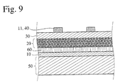
Fig. 9 is a partial cross sectional view showing a preferable structure of a
photoelectric conversion device of the present invention.
DETAILED DESCRIPTION OF THE PREFERRED EMBODIMENTS
[1] Photoelectric Conversion Device
A photoelectric conversion device of the present invention comprises: an
electrically conductive layer; a photosensitive layer containing a semiconductor
fine particle on which a dye is adsorbed; a charge transfer layer; and a counter
electrode. The dye is treated with a treatment solution composed of a
quaternary salt and a solvent before or after the dye is adsorbed on the
semiconductor fine particle, to improve photoelectric conversion efficiency of
the photoelectric conversion device.
As shown in Fig. 1, the photoelectric conversion device of the present
invention preferably comprises: an electrically conductive layer 10; a
photosensitive layer 20 containing semiconductor fine particles 21 sensitized by
dyes 22 and an charge-transporting material 23 penetrated into voids among the
particles; a charge transfer layer 30; and a counter electrically conductive layer
40 laminated in this order. An undercoating layer 60 may be disposed between
the electrically conductive layer 10 and the photosensitive layer 20. The
charge-transporting material 23 is generally the same as the material used for the
charge transfer layer 30. On the electrically conductive layer 10 and/or the
counter electrically conductive layer 40 may be disposed a substrate 50 to
improve the strength of the photoelectric conversion device. Hereinafter in the
present invention, a layer composed of the electrically conductive layer 10 and
the substrate 50 disposed thereon if necessary is referred to as "conductive
support", and a layer composed of the counter electrically conductive layer 40
and the substrate 50 disposed thereon if necessary is referred to as "counter
electrode". A photoelectric cell is constituted by connecting the photoelectric
conversion device to an external circuit to electrically work or generate
electricity in the external circuit. A photosensor is such a photoelectric
conversion device as sensing optical information. Incidentally, the electrically
conductive layer 10, the counter electrically conductive layer 40 and the
substrate 50 shown in Fig. 1 may be a transparent electrically conductive layer
10a, a transparent counter electrically conductive layer 40a and a transparent
substrate 50a, respectively.
In the photoelectric conversion device shown in Fig. 1, a light injected to
the photosensitive layer 20 excites the dye 22, etc., excited high energy electrons
therein are transported to a conduction band of the semiconductor fine particles
21, and they are diffused to reach to the electrically conductive layer 10. At
this time, the dye 22 is in oxidized form. In the case of a photoelectric cell
composed of the photoelectric conversion device, electrons in the electrically
conductive layer 10 are returned to the oxidized dye through the counter
electrically conductive layer 40 and the charge transfer layer 30 while working
in the external circuit, so that the dye 22 is regenerated. In a boundary of each
layer such as a boundary between the electrically conductive layer 10 and the
photosensitive layer 20, a boundary between the photosensitive layer 20 and the
charge transfer layer 30, a boundary between the charge transfer layer 30 and the
counter electrically conductive layer 40, etc., components of each layer may be
diffused and mixed.
A method for treating the dye with the treatment solution, and
components and structures of the photoelectric conversion device of the present
invention will be explained in detail below without intention of restricting the
scope of the present invention.
(A) Method for Treating Dye
The dye is treated with the treatment solution composed of the
quaternary salt and the solvent. The treatment solution may be so-called
dispersion. In the present invention, the term "the dye is treated with the
treatment solution" means that the dye is made to come into contact with the
treatment solution for a predetermined period. The predetermined period is not
particularly limited, and generally 30 seconds to 24 hours. The dye may be
treated with the treatment solution before or after the dye is adsorbed on the
semiconductor fine particle, thus, the entire photosensitive layer may be treated
with the treatment solution. Further, it does not matter whether the quaternary
salt is adsorbed on the dye or not after the treatment. The quaternary salt may
interact with the dye to provide an ion-exchanged product.
The treatment solution contains at least the quaternary salt and the
solvent, and may contain other additives. The quaternary salt used in the
present invention includes at least a nitrogen atom or a phosphorus atom, which
has positive formal charge and is not directly connected to a hydrogen atom.
Specific examples of the quaternary salt include quaternary ammonium salts,
imidazolium salts, oxazolium salts, thiazolium salts, benzimidazolium salts,
pyridinium salts, pyrazinium salts, quinolinium salts, quaternary phosphonium
salts, etc. Among them, preferred are tetralkylammonium salts, imidazolium
salts and pyridinium salts, more preferred are tetralkylammonium salts having a
cyclic structure, imidazolium salts and pyridinium salts. The quaternary salt
may include multivalent cationic moiety composed of 2 or more cationic groups
connected to each other.
The quaternary salt preferably has at least one alkyl group containing 6
or more carbon atoms such as a hexyl group, an octyl group, a dodecyl group,
etc. Such an alkyl group may have a substituent, examples thereof including
halogen atoms, alkyl groups that may be a cycloalkyl group or a bicycloalkyl
group, alkenyl groups that may be a cycloalkenyl group or a bicycloalkenyl
group, alkynyl groups, aryl groups, heterocyclic groups, cyano group, hydroxyl
group, nitro group, carboxyl group, alkoxy groups, aryloxy groups, silyloxy
groups, heterocyclic oxy groups, acyloxy groups, carbamoyloxy groups,
alkoxycarbonyloxy groups, aryloxycarbonyloxy groups, amino groups that may
be anilino group, acylamino groups, aminocarbonylamino groups,
alkoxycarbonylamino groups, aryloxycarbonylamino groups, sulfamoylamino
groups, alkylsulfonylamino groups, arylsulfonylamino groups, mercapto groups,
alkylthio groups, arylthio groups, heterocyclic thio groups, sulfamoyl groups,
sulfo group, alkylsulfinyl groups, arylsulfinyl groups, alkylsulfonyl groups,
arylsulfonyl groups, acyl groups, aryloxycarbonyl groups, alkoxycarbonyl
groups, carbamoyl group, arylazo groups, heterocyclic azo groups, imide
groups, phosphono group, phosphonyl group, phosphonyloxy group,
phosphonylamino groups, silyl group, etc.
The quaternary salt may include organic or inorganic anion. Examples
thereof include: halide ions such as a fluoride ion, a chloride ion, a bromide ion
and iodide ion; perchlorate ion; tetrafluoroborate ion, hexafluorophosphate ion,
acetate ion, trifluoroacetate ion, methanesulfonate ion, p-toluene sulfonate ion,
trifluoromethane sulfonate ion, bis(trifluoromethane sulfonyl)imide ion,
tris(trifluoromethane sulfonyl)methide ion, etc. The quaternary salt may be an
inner salt.
The quaternary salt preferably has a pyridyl group. The pyridyl group
may have a substituent with examples being the same as those of the above-mentioned
substituent on the alkyl group containing 6 or more carbon atoms.
The quaternary salt having a pyridyl group is particularly preferably
represented by the following general formula (I):
In the general formula (I), Q represents a quaternary ammonium salt
moiety. The quaternary ammonium salt moiety may be a monovalent group
generated by removing a hydrogen atom from a salt such as a
tetralkylammonium salt, an imidazolium salt, an oxazolium salt, a thiazolium
salt, a benzimidazolium salt, a pyridinium salt, a pyrazinium salt, a quinolinium
salt, etc. The quaternary ammonium salt moiety is preferably a monovalent
group generated from a tetralkylammonium salt (a tetralkylammonium salt
moiety), particularly preferably a monovalent group generated from a
tetralkylammonium salt having at least one alkyl group containing 6 or more
carbon atoms such as a hexyl group, an octyl group, a dodecyl group, etc.
Q generally includes organic or inorganic anion. Examples of the anion
include: halide ions such as a fluoride ion, a chloride ion, a bromide ion and
iodide ion; a perchlorate ion; a tetrafluoroborate ion, a hexafluorophosphate ion,
an acetate ion, trifluoroacetate ion, a methanesulfonate ion, a p-toluene sulfonate
ion, a trifluoromethane sulfonate ion, bis(trifluoroethane sulfonyl)imide ion,
tris(trifluoromethane sulfonyl)methide ion, etc. Among them, particularly
preferred is iodide ion. Q may be an inner salt moiety.
In the general formula (I), LINK represents a divalent linking group.
The divalent linking group may have a substituent with examples being the same
as those of the above-mentioned substituent on the alkyl group containing 6 or
more carbon atoms. Examples of the divalent linking group include:
substituted or unsubstituted alkylene groups such as methylene group, ethylene
group, propylene group and hexylene group; substituted or unsubstituted arylene
groups such as phenylene group and naphtylene group; -O-; -S-; carbonyl group;
substituted or unsubstituted imino groups such as imino group, methylimino
group and phenylimino group; sulfonyl group; combinations thereof; etc. Of
these groups, particularly preferred are alkylene groups.
In the general formula (I), R1 represents a substituent with examples
being the same as those of the above-mentioned substituent on the alkyl group
containing 6 or more carbon atoms. R1 is preferably an alkyl group such as
methyl group, ethyl group, 2-propyl group, t-butyl group, hexyl group and
dodecyl group.
In the general formula (I),
n1 represents an integer of 0 to 4, preferably
represents an integer of 0 to 2.
n2 represents 0 or 1. Specific examples of the
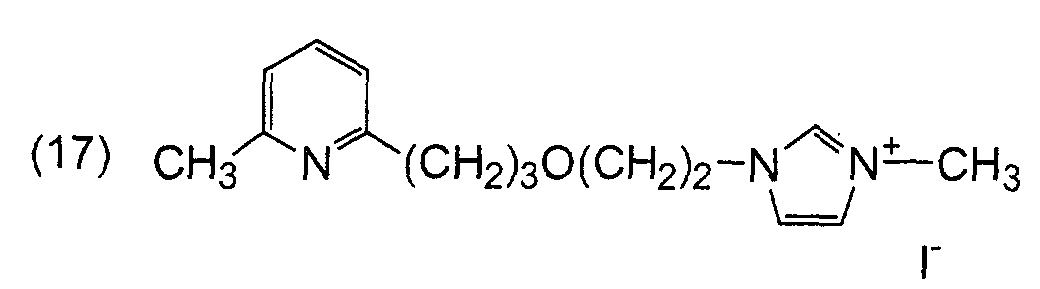
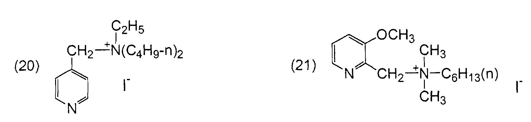
quaternary salt represented by the general formula (I) will be illustrated below
without intention of restricting the scope of the present invention defined by the
claims attached hereto.
The quaternary salts shown below are also preferably used in the present
invention.
(25) (CH3)4N+ Cl-
(26) (C2H5)4N+ Br-
(27) (C4H9)4N+ I-
(28) (C6H13)4N+ I-
(29) (C7H15)4N+ ClO4 -
(31) n-C16H33N+(CH3)3 BF4 -
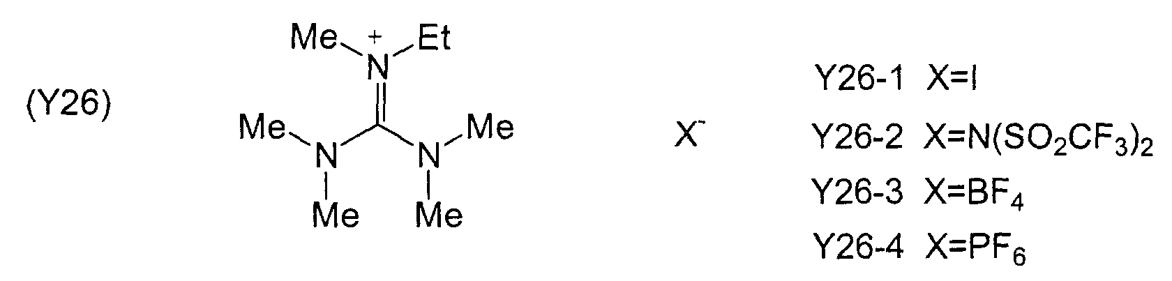
(46) (C4F9CH2CH2)4-N+ I- The solvent may be appropriately selected depending on the solubility of
the quaternary salt. Examples of the solvent include: alcohols such as
methanol, ethanol, t-butanol and benzyl alcohol; nitrile compounds such as
acetonitrile, propionitrile and 3-methoxypropionitrile; nitromethane; halogenated
hydrocarbons such as dichloromethane, dichloroethane, chloroform and
chlorobenzene; ethers such as diethylether and tetrahydrofuran;
dimethylsulfoxide; amides such as N,N-dimethylformamide and N,N-dimethylacetamide;
N-methylpyrrolidone; 1,3-dimethylimidazolidinone; 3-methyloxazolidinone;
esters such as ethyl acetate and butyl acetate; carbonates
such as diethyl carbonate, ethylene carbonate and propylene carbonate; ketones
such as acetone, 2-butanone and cyclohexanone; hydrocarbons such as hexane,
petroleum ether, benzene and toluene; and mixtures thereof. Among them, the
solvent is preferably a nitrile compound.
To the treatment solution containing the quaternary salt may be added an
additive. Typical examples of the additive include carboxylated steroidal
compounds such as chenodeoxycholic acid and cholic acid, ultraviolet-absorbing
agents, surfactants, etc.
The concentration of the quaternary salt in the treatment solution is
preferably 1 × 10⁻⁴ to 1 mol/l, more preferably 1 x 10⁻³ to 2 x 10⁻¹ mol/l. The
molecularity of the quaternary salt in the treatment solution is equivalent to or
more than the total number of acidic group, which will be described in detail
below, of the dye in the photosensitive layer.
Although treated with the treatment solution may be the photosensitive
layer or only the dye that is not yet adsorbed on the semiconductor fine particle,
it is preferable that the photosensitive layer is treated with the treatment
solution.
Method for treating the photosensitive layer with the treatment solution
is not particularly limited if only it can efficiently make the treatment solution
come into contact with the dye-adsorbed semiconductor fine particle. The
method may be a soaking method, a coating method, a spraying method, etc.
Of these, preferred is a soaking method. In the soaking method, temperature of
the treatment solution and soaking period may be optionally controlled. In a
typical embodiment, the photosensitive layer is soaked in the treatment solution
at 20 to 80 °C for 30 seconds to 24 hours. After soaking, although the
photosensitive layer may be immediately dried, it is preferable that the
photosensitive layer is washed with a solvent. The solvent for washing the
photosensitive layer is preferably such that same as the solvent for the treatment
solution, or a polar solvent such as a nitrile compound, an alcohol, etc.
In the case where the dye is treated with the treatment solution before the
dye is adsorbed on the semiconductor fine particle, for example, the dye may be
dissolved in the treatment solution to isolate a salt composed of the dye and a
cation moiety of the quaternary salt.
(B) Photosensitive Layer
The photosensitive layer contains the semiconductor fine particle on
which the dye is adsorbed. In the photosensitive layer, the semiconductor fine
particle acts as a photosensitive substance to absorb a light and conduct charge
separation, thereby generating electrons and positive holes. With respect to the
dye-sensitized semiconductor fine particle, the light absorption and the
generation of the electrons and the positive holes are primarily caused in the dye,
and the semiconductor fine particle receives and conveys the electrons or the
positive holes.
(1) Semiconductor
Used as the semiconductor may be: an elementary substance
semiconductor such as silicon and germanium; a III-V series compound
semiconductor; a metal chalcogenide such as a metal oxide, a metal sulfide, a
metal selenide and a composite thereof; a compound having a perovskite
structure such as strontium titanate, calcium titanate, sodium titanate, barium
titanate and potassium niobate; etc. An n-type semiconductor is preferably
used in the present invention, in which conductor electrons act as a carrier under
photo-excitation condition to provide anode current.
Preferable examples of the metal chalcogenide include: oxide of
titanium, tin, zinc, iron, tungsten, zirconium, hafnium, strontium, indium,
cerium, yttrium, lanthanum, vanadium, niobium or tantalum; sulfide of
cadmium, zinc, lead, silver, antimony or bismuth; selenide of cadmium or lead;
cadmium telluride; etc. Additionally, the other compound semiconductors such
as phosphides of zinc, gallium, indium or cadmium, selenides of gallium-arsenic
or copper-indium, copper-indium sulfide, etc. may be used in this invention.
Further, composite semiconductors such as MxOySz and M1xM2yOz are also
preferably used in the present invention, wherein M, M1 and M2 independently
represent a metal atom, O represents an oxygen atom, S represents a sulfur atom,
and x, y and z represent numbers combined with each other to form a neutral
molecule.
Preferable specific examples of the semiconductor include Si, TiO2,
SnO2, Fe2O3, WO3, ZnO, Nb2O5, CdS, ZnS, PbS, Bi2S3, CdSe, CdTe, SrTiO3,
GaP, InP, GaAs, CuInS2 and CuInSe2. Of these semiconductors, more
preferred are TiO2, SnO2, Fe2O3, WO3, ZnO, Nb2O5, CdS, PbS, CdSe, SrTiO3,
InP, GaAs, CuInS2 and CuInSe2, particularly preferred are TiO2 and Nb2O5, and
the most preferred is TiO2. TiO2 used in the present invention contains
anatase-type crystal structure of preferably 70 volume % or more, particularly
preferably 100 volume %. It is preferable that the semiconductor is doped with
a divalent or trivalent metal, to increase electron conductivity thereof. Further,
the semiconductor is preferably doped with a monovalent metal to prevent a
reverse current from being provided from the semiconductor to the charge
transfer layer.
The semiconductor may have a single crystal or poly crystal structure.
The poly crystal semiconductor is preferred from the viewpoints of the
production cost, the security of the raw materials, the energy-payback time, etc.
The photosensitive layer is particularly preferably a porous semiconductor fine
particle layer. The photosensitive layer may partly contain an amorphous
semiconductor.
The particle size of the semiconductor fine particle is generally in the nm
to µm level. The mean size of primary semiconductor particles, which is
obtained from a diameter of a circle equivalent to a projected area thereof, is
preferably 5 to 200 nm, more preferably 8 to 100 nm. Further, the mean size of
secondary semiconductor particles in dispersion is preferably 0.01 to 30 µm.
Two or more of the semiconductor fine particles having a different
particle size distribution may be mixed to use for the photosensitive layer. In
this case, the average particle size of the smaller particles is preferably 25 nm or
less, more preferably 10 nm or less. To improve a light-capturing rate of the
photoelectric conversion device by scattering ray of incident light, the
semiconductor fine particles having a large particle size, e.g. approximately 300
nm in diameter, may be used for the photosensitive layer.
Two or more kinds of the semiconductor fine particles may be used for
the photosensitive layer. In this case, it is preferable that one is TiO2, ZnO,
Nb2O5 or SrTiO3 and the other is SnO2, Fe2O3 or WO3. More preferred
combination is ZnO and SnO2, ZnO and WO3, ZnO, SnO2 and WO3, etc. Each
of the semiconductor fine particles may have a different diameter. Particularly
preferred is a combination of TiO2, ZnO, Nb2O5 or SrTiO3 having a larger
diameter and SnO2, Fe2O3 or WO3 having a smaller diameter. The larger
diameter is preferably 100 nm or more, and the smaller diameter is preferably 15
nm or less.
Preferred as a method for producing the semiconductor fine particles are:
sol-gel methods described in Sumio Sakka, "Zoru-Geru-Ho No Kagaku (Science
of Sol-Gel Method)", Agune Shofusha (1998), Technical information
Association, "Zoru-Geru-Ho Niyoru Hakumaku Coating Gijutu (Thin Film-Coating
Technology by Sol-Gel Method)" (1995), etc.; and gel-sol methods
described in Tadao Sugimoto, "Shin-Goseiho Geru-Zoru-Ho Niyoru
Tanbunsanryusi No Gosei To Saizu-Keitaiseigyo (Synthesis of Mono-Dispersion
Particles and Control of Their Size and Form by Novel Gel-Sol Method)", and
MATERIA, Vol. 35, No. 9, Page 1012 to 1018 (1996). The method developed
by Degussa Company, which comprises preparing oxides by subjecting
chlorides to a high temperature hydrolysis in an oxyhydrogen salt, is also
preferred.
In the case of using titanium oxide as the semiconductor fine particles,
any of the above-described sol-gel methods, gel-sol methods and high
temperature hydrolysis method are preferably used, further, a sulfuric acid
method and a chlorine method described in Manabu Seino, "Sanka-Chitan Bussei
To Ouyougijutu (Titanium oxide - Properties and Applied Technique)", Gihodo
Shuppan, (1997) may be used. Of the sol-gel methods, also preferred are such
that described in Christophe J. Barb'e, et al, Journal of American Ceramic
Society, Vol. 80, No. 12, Page 3157 to 3171 (1997) and Burnside, et al,
Chemistry of Materials, Vol. 10, No. 9, Page 2419 to 2425.
(2) Semiconductor Fine Particle Layer
The semiconductor fine particles may be applied onto the conductive
support by: a method where the conductive support is coated with a dispersion or
a colloidal solution containing the particles; the above-mentioned sol-gel
method; etc. A wet type film production method is relatively advantageous for
the mass production of the photoelectric conversion device, improvement of
properties of the semiconductor fine particle solution and the adaptability of the
conductive support, etc. As such a wet type film production method, coating
methods, printing methods, electrolytic deposition methods and
electrodeposition techniques are typical examples. Further, the semiconductor
fine particle layer may be disposed by: oxidizing a metal; an LPD method where
a metal solution is subjected to ligand exchange, etc.; a sputtering method; a
vapor deposition method; a CVD method; or an SPD method where a thermal
decomposition-type metal oxide precursor is sprayed on a heated substrate to
generate a metal oxide.
The dispersion containing the semiconductor fine particles may be
prepared by: the sol-gel methods mentioned above; crushing the semiconductor
in a mortar; dispersing the semiconductor while grinding it in a mill;
synthesizing and precipitating the semiconductor fine particles in a solvent; etc.
As a dispersion solvent, water or organic solvents such as methanol,
ethanol, isopropyl alcohol, citronellol, terpineol, dichloromethane, acetone,
acetonitrile, ethyl acetate, etc. may be used. A polymer such as polyethylene
glycol, hydroxyethylcellulose and carboxymethylcellulose, a surfactant, an acid,
a chelating agent, etc. may be used as a dispersing agent, if necessary. In
particular, it is preferable that polyethylene glycol is added to the dispersion
because the viscosity of the dispersion and the porosity of the semiconductor
fine particle layer can be controlled by changing the molecular weight of the
polyethylene glycol, and the semiconductor fine particle layer containing
polyethylene glycol is hardly peeled off.
Preferred coating methods include: a roller method and a dip method as
an application series; an air-knife method and a blade method as a metering
series; etc. Further, preferable as a method where an application and metering
can be performed at the same time are a wire-bar method disclosed in JP-B-58-4589,
a slide-hopper method described in United States Patent Nos. 2,681,294,
2,761,419, 2,761,791, etc., an extrusion method, a curtain method, etc.
Furthermore, as for a wide use, a spin method and a spray method are preferred.
As a wet type printing method, three major printing methods of a relief printing,
an offset printing and a gravure printing, an intaglio printing, a gum printing, a
screen printing, etc. are preferred. A preferable film production method may be
selected from these methods in accordance with the viscosity of the dispersion
and the desired wet thickness.
The semiconductor fine particle layer is not limited to a single layer.
The dispersions each comprising the semiconductor fine particles having a
different particle size may be subjected to a multi-layer coating. Further, the
dispersions each containing different kinds of semiconductor fine particles,
binder or additives may be subjected to a multi-layer coating. The multi-layer
coating is also effectively used when the thickness of the layer is insufficient by
coating of once.
Generally, when the thickness of the semiconductor fine particle layer,
equal to the thickness of the photosensitive layer, becomes thicker, the amount
of the dye incorporated therein per unit of the projected area increases, to make
the light capturing rate higher. However, because diffusion distances of the
generated electrons are increased in this case, loss owing to recombination of the
electric charges is also increased. Consequently, the preferable thickness of the
semiconductor fine particle layer is 0.1 to 100 µm. In the case of the
photoelectric cell, the thickness of the semiconductor fine particle layer is
preferably 1 to 30 µm, more preferably 2 to 25 µm. A coating amount of the
semiconductor fine particles per 1 m2 of the support is preferably 0.5 to 100 g,
more preferably 3 to 50 g.
After coating the semiconductor fine particles on the conductive support,
the particles are preferably subjected to a heat treatment, to electronically contact
them with each other and to increase the coating strength and the adherence
thereof with the support. The heating temperature is preferably 40 to 700 °C,
more preferably 100 to 600 °C. The heating time is preferably 10 minutes to
10 hours. It is not preferred that the substrate having low melting point or
softening point such as a polymer film is subjected to a high temperature
treatment because such a substrate tends to be deteriorated thereby. The heat
treatment is preferably carried out at a temperature as low as possible, for
example, 50 to 350 °C, also from the viewpoint of cost. The semiconductor
fine particle layer containing the smaller semiconductor fine particles having a
size of 5 nm or less, a mineral acid, a metal oxide precursor, etc. can be heat-treated
at such a low temperature. Further, the heat treatment may be carried
out while applying ultraviolet ray, infrared ray, microwave, electric field,
ultrasonic wave, etc. to the semiconductor fine particles, to reduce the heating
temperature. To remove unnecessary organic compounds, the heat treatment is
preferably carried out in combination with evacuation, oxygen plasma treatment,
washing by pure water, a solvent or a gas, etc.
After the heat treatment, the semiconductor fine particle layer may be
subjected to a chemical metal-plating using an titanium tetrachloride aqueous
solution, etc. or an electrochemical metal-plating using an titanium trichloride
aqueous solution, etc., to increase the surface area of the semiconductor fine
particles, or to enhance a purity of the particles, thereby improving the electron-injecting
efficiency into the particles from the dye. Further, to prevent a
reverse current from being provided from the semiconductor fine particles to the
charge transfer layer, on the semiconductor fine particles is preferably adsorbed
an organic compound having low electron conductivity. The organic
compound preferably has a hydrophobic group.
It is preferable that the semiconductor fine particle layer has a large
surface area to adsorb lots of dyes. Therefore, the surface area of the
semiconductor fine particle layer is preferably 10 times or more, more preferably
100 times or more of its projected area. The highest limit, even though it is not
limited in particular, is generally a level of 1000 times.
(3) Dye
The dye used for the photosensitive layer is not particularly limited if it
can absorb a light in visible region, near infrared region, etc. and can sensitize
the semiconductor fine particle. The dye is preferably selected from the group
consisting of metal complex dyes, methine dyes, porphyrin dyes and
phthalocyanine dyes, and particularly preferably a ruthenium complex dye
and/or a methine dye. To make the photoelectric conversion wave range of the
photoelectric conversion device larger, and to increase the photoelectric
conversion efficiency, two or more kinds of the dyes are preferably used as a
mixture or in combination thereof. In the case of using two or more kinds of
the dyes, the kinds and the ratio of the dyes may be selected in accordance with
the wave range and the strength distribution of the light source.
The dye preferably has an interlocking group, which can interact or
adsorb to the surface of the semiconductor fine particles. Preferred
interlocking groups include acidic groups such as -COOH, -OH, -SO3H,-P(O)(OH)2
and -OP(O)(OH)2, and π-conductive chelating groups such as oxime
group, dioxime group, hydroxyquinoline group, salicylate group and α-ketoenolate
group. Among them, preferred are acidic groups, particularly
preferred are -COOH, -P(O)(OH)2 and -OP(O)(OH)2. The interlocking group
may form a salt with an alkaline metal, etc. or an intramolecular salt. In the
polymethine dye, an acidic group such as squarylium ring group or croconium
ring group formed by the methine chain may act as the interlocking group.
The preferred dyes used for the photosensitive layer will be specifically
described below.
(a) Metal Complex Dye
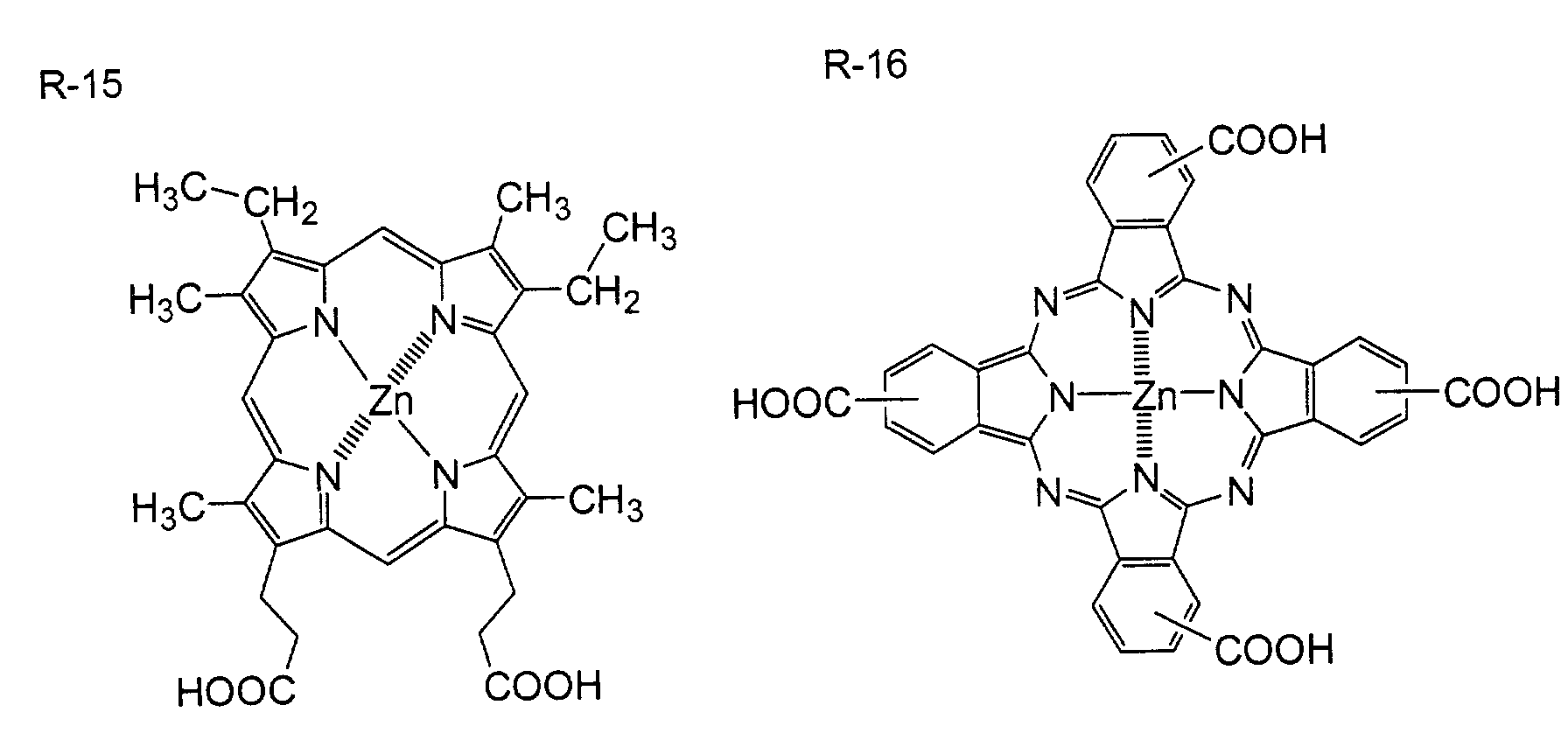
The metal complex dye used in the present invention is preferably a
metallophthalocyanine dye, a metal porphyrin dye or a ruthenium complex dye,
particularly preferably a ruthenium complex dye. The ruthenium complex dyes
described in United States Patent Nos. 4,927,721, 4,684,537, 5,084,365,
5,350,644, 5,463,057 and 5,525,440, Japanese Patent Laid-Open Nos. 7-249790
and 2000-26487, Japanese Patent Publication No. 10-504512, WO 98/50393,
etc. may be used in the present invention.
The ruthenium complex dye used in the present invention is preferably
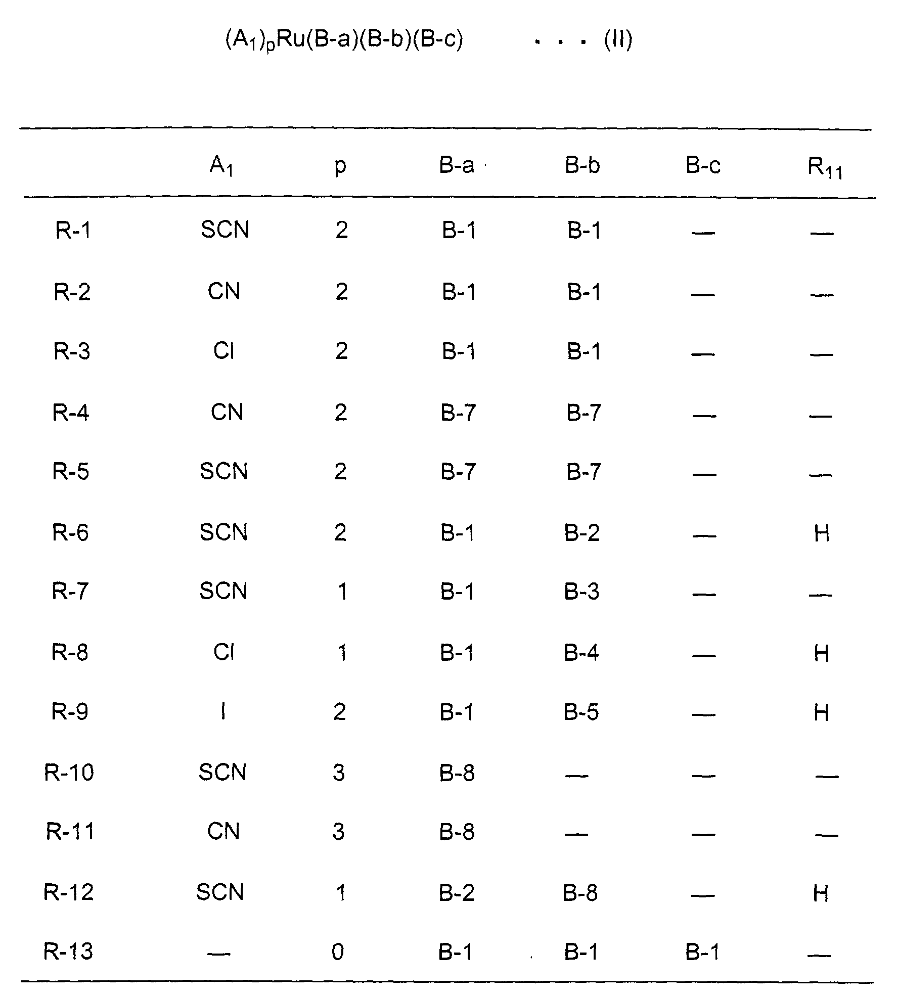
represented by the following general formula (II):
(A1)pRu(B-a)(B-b)(B-c)
In the general formula (II),
A1 represents a monovalent or divalent
ligand.
A1 is preferably selected from the group consisting of Cl, SCN, H
2O,
Br, I, CN, NCO, SeCN, β-diketone derivatives, oxalic acid derivatives and
dithiocarbamic acid derivatives.
p is an integer of 0 to 3.
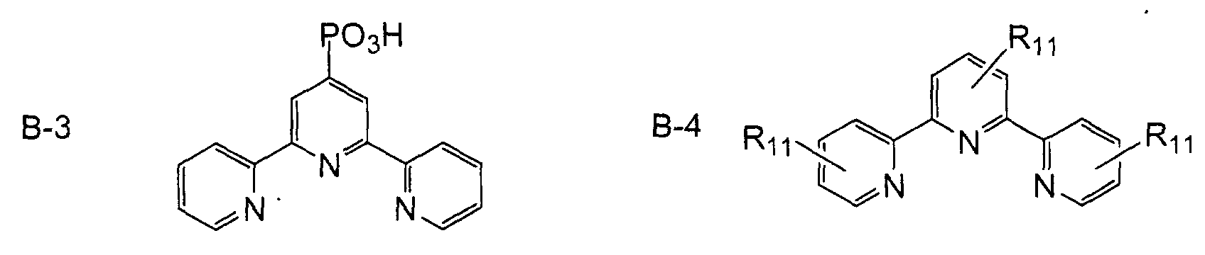
B-a,
B-b, and
B-c
independently represent an organic ligand represented by any of the following
formulae
B-1 to
B-10.
In the formulae B-1 to B-10, R11 represents a hydrogen atom or a
substituent. Specific examples of the substituent include: halogen atoms;
substituted or unsubstituted alkyl groups having 1 to 12 carbon atom; substituted
or unsubstituted aralkyl groups having 7 to 12 carbon atoms; substituted or
unsubstituted aryl groups having 6 to 12 carbon atoms; acidic groups that may
form a salt such as carboxyl group and phosphono group; etc. The alkyl group
and the alkyl moiety of the aralkyl group may be straight or branched, and the
aryl group and the aryl moiety of the aralkyl group may have a monocyclic
structure or a polycyclic structure such as a condensed ring and a ring
assemblage. B-a, B-b and B-c may be the same or different ligands, and the
ruthenium complex dye represented by the general formula (II) may have only
one or two of B-a, B-b and B-c.
The metal complex dyes preferably used in the present invention will be
illustrated below without intention of restricting the scope of the present
invention defined by the claims attached hereto.
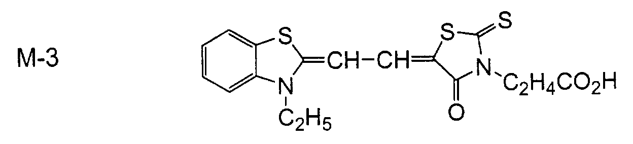
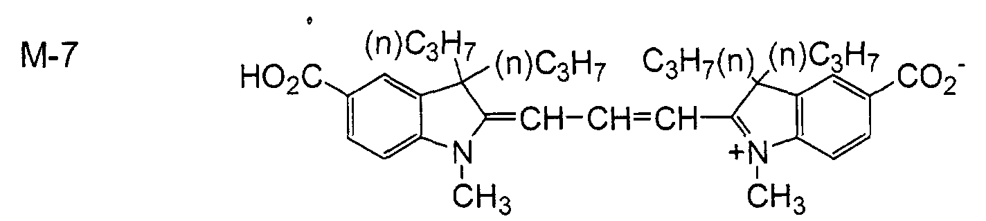
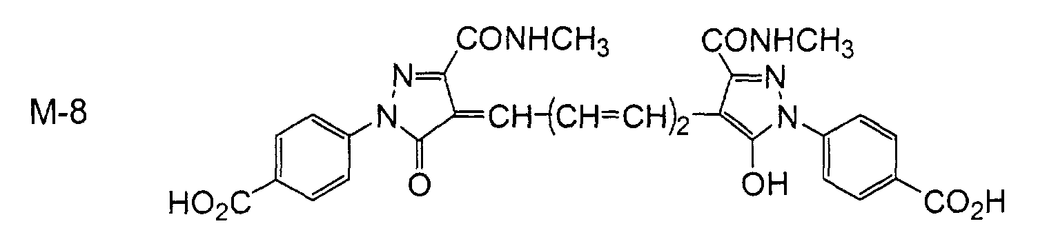
The methine dye used in the present invention is preferably a
polymethine dye such as a cyanine dye, a merocyanine dye, a squalilium dye,
etc. The polymethine dyes disclosed in Japanese Patent Laid-Open Nos. 11-35836,
11-67285, 11-86916, 11-97725, 11-158395, 11-163378, 11-214730, 11-214731
and 11-238905, European Patent Nos. 892411 and 911841 are
preferably used in the present invention. Specific examples of the methine dye
are shown below.
The dye may be adsorbed to the semiconductor fine particles by soaking
the conductive support having the well-dried semiconductor fine particle layer in
a dye adsorption solution, or by applying the dye adsorption solution to the
semiconductor fine particle layer. In the former case, a soaking method, a
dipping method, a roller method, an air-knife method, etc. may be used. In the
soaking method, the dye may be adsorbed at a room temperature or under reflux
as described in Japanese Patent Laid-Open No. 7-249790. As an applying
method of the latter case, a wire-bar method, a slide-hopper method, an
extrusion method, a curtain method, a spin method, a spray method, etc. may be
used.
Examples of a solvent for the dye adsorption solution include: alcohols
such as methanol, ethanol, t-butanol and benzyl alcohol; nitrile compounds such
as acetonitrile, propionitrile and 3-methoxypropionitrile; nitromethane;
halogenated hydrocarbons such as dichloromethane, dichloroethane, chloroform
and chlorobenzene; ethers such as diethylether and tetrahydrofuran;
dimethylsulfoxide; amides such as N,N-dimethylformamide and N,N-dimethylacetamide;
N-methylpyrrolidone; 1,3-dimethylimidazolidinone; 3-methyloxazolidinone;
esters such as ethyl acetate and butyl acetate; carbonates
such as diethyl carbonate, ethylene carbonate and propylene carbonate; ketones
such as acetone, 2-butanone and cyclohexanone; hydrocarbons such as hexane,
petroleum ether, benzene and toluene; and mixtures thereof.
The total amount of the dye is preferably 0.01 to 100 mmol per the unit
surface area (1 m2) of the conductive support. The amount of the dye adsorbed
on the semiconductor fine particles is preferably 0.01 to 1 mmol per 1 g of the
semiconductor fine particles. Such an adsorption amount of the dye effects a
sufficient sensitization to the semiconductors. Too small amount of the dye
results in insufficient sensitization effect. On the other hand, if the amount of
the dye is excessive, the dye unadsorbed on the semiconductor fine particles
floats to reduce the sensitization effect.
To increase the adsorption amount of the dye, it is preferable that the
semiconductor fine particle layer is subjected to a heat treatment before the dye
is adsorbed thereon. After the heat treatment, it is preferable that the dye is
quickly adsorbed on the semiconductor fine particle layer having a temperature
of 60 to 150 °C before the layer is cooled to the room temperature, to prevent
water from adsorbing onto the semiconductor fine particle layer.
To weaken an interaction between the dyes such as association, a
colorless compound may be co-adsorbed onto the semiconductor fine particles
together with the dye. The colorless compound preferably has surface activity,
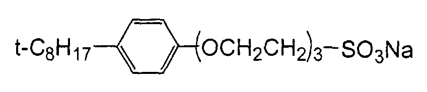
and examples thereof include steroid compounds having a carboxyl group such
as chenodeoxycholic acid, and sulfonates shown below.
The dye unadsorbed on the semiconductor fine particle layer is
preferably removed by washing immediately after the dye adsorption process.
The washing is preferably carried out by a wet-type washing bath with a polar
solvent such as acetonitrile or an organic solvent such as an alcohol solvent.
The surface of the semiconductor fine particles may be treated with an amine
compound or a quaternary salt after the dye adsorption process. The amine
compound is preferably pyridine, 4-t-butylpyridine, polyvinylpyridine, etc., and
the quaternary salt is preferably tetrabutylammonium iodide,
tetrahexylammonium iodide, etc. The amine compound and the quaternary salt
may be used singly when it is liquid, and may be used in a fashion of a solution
in an organic solvent.
(C) Conductive Support
The conductive support is composed of (1) a single layer of the
electrically conductive layer, or (2) two layers of the electrically conductive
layer and the substrate. In the case of (1), the electrically conductive layer is
preferably made of a material that has a sufficient strength and can sufficiently
seal the photoelectric conversion device, for example, a metal such as platinum,
gold, silver, copper, zinc, titanium, aluminum and an alloy composed thereof.
In the case of (2), the substrate on which the electrically conductive layer
containing an electrically conductive material is disposed at the photosensitive
layer side may be used as the conductive support. Preferable examples of the
electrically conductive material include: metals such as platinum, gold, silver,
copper, zinc, titanium, aluminum, indium and alloys composed thereof; carbon;
electrically conductive metal oxides such as indium-tin composite oxides and tin
oxides doped with fluorine; etc. The electrically conductive layer preferably
has a thickness of 0.02 to 10 µm.
The surface resistance of the conductive support is preferably as low as
possible. The surface resistance is preferably 50 Ω/square or less, more
preferably 20 Ω/square or less.
When light is irradiated from the conductive support side, it is preferred
that the conductive support is substantially transparent. Herein, the term
"substantially transparent" means that the light transmittance is 10 % or more to
a light in visible region to near infrared region (400 to 1200 nm). The light
transmittance is preferably 50 % or more, more preferably 80 % or more. The
conductive support particularly preferably has high light transmittance to a light
which the photosensitive layer has sensitivity to.
The transparent conductive support is preferably constituted by disposing
the transparent electrically conductive layer of an electrically conductive metal
oxide on the transparent substrate of such material as a glass and a plastic by
coating or vapor deposition. The transparent electrically conductive layer is
preferably made of tin dioxide doped with fluorine or antimony, or indium-tin
oxide (ITO). The transparent substrate may be made of a glass such as low-cost
soda glass excellent in strength and non-alkali glass that is not affected by
alkaline elution. Additionally, a transparent polymer film is preferably used as
the transparent substrate. Used as the materials for the transparent polymer
film may be tetracetylcellulose (TAC), polyethylene terephthalate (PET),
polyethylene naphthalate (PEN), syndiotactic polystyrene (SPS),
polyphenylenesulfide (PPS), polycarbonate (PC), polyarylate (PAr), polysulfone
(PSF), polyestersulfone (PES), polyimide (PI), polyetherimide (PEI), cyclic
polyolefin, brominated phenoxy, etc. To secure a sufficient transparency, the
coating amount of the electrically conductive metal oxide is preferably 0.01 to
100 g per 1 m2 of the glass or plastic substrate.
It is preferable that a metal lead is used to reduce the resistance of the
transparent conductive support. The metal lead is preferably made of a metal
such as platinum, gold, nickel, titanium, aluminum, copper, silver, etc. It is
preferable that the metal lead is provided on the transparent substrate by a vapor
deposition method, a sputtering method, etc., the transparent electrically
conductive layer of conductive tin oxide or ITO being disposed thereon. The
reduction in incident light quantity owing to the metal lead is suppressed to
preferably 10 % or less, more preferably 1 to 5 %.
(D) Charge Transfer Layer
The charge transfer layer replenishes electrons to the oxidized dye. The
charge transfer layer may be composed of (i) an ion conductive electrolyte
composition or (ii) a carrier-mediated, charge-transporting material utilizing
charge transport mediated by a carrier in solid. Examples of (i) the ion
conductive electrolyte composition include: molten salt electrolyte compositions
containing a redox couple; electrolysis solutions where a redox couple is
dissolved in a solvent; so-called gel electrolyte compositions where a solution
including a redox couple is penetrated into a polymer matrix; solid electrolyte
compositions; etc. Examples of (ii) the carrier-mediated, charge-transporting
material include electron-transporting materials and hole-transporting materials.
These materials may be used in combination with each other.
(1) Molten Salt Electrolyte Composition
The molten salt electrolyte compositions are particularly preferably used
for the charge transfer layer from the viewpoint of improving the durability and
the photoelectric conversion efficiency of the photoelectric conversion device.
The molten salt electrolyte composition comprises a molten salt electrolyte
having a low melting point. In the present invention, pyridinium salts,
imidazolium salts and triazolium salts disclosed in WO 95/18456, Japanese
Patent Laid-Open No. 8-259543, "Denki Kagaku (Electrochemistry)", 65, 11,
923 (1997), etc. may be used as the molten salt electrolyte. The molten salt
electrolyte preferably has the melting point of 100 °C or less, and it is
particularly preferably liquid at the room temperature.
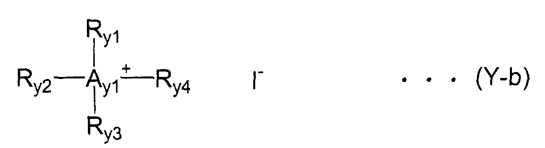
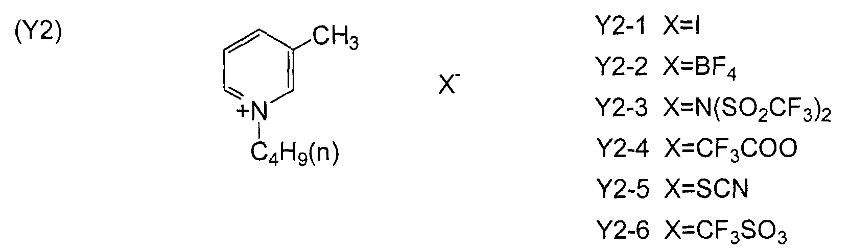
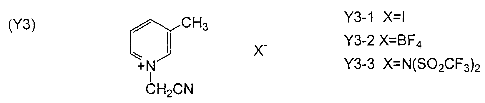
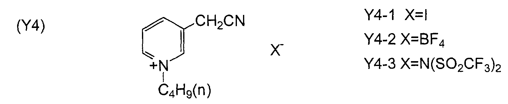
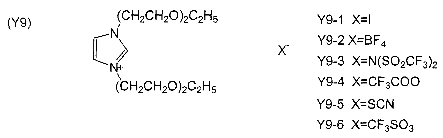
The molten salt electrolytes represented by any of the following general
formulae
(Y-a),
(Y-b) and
(Y-c) can be preferably used in the present invention.
In the general formula (Y-a), Qy1 represents an atomic group forming an
aromatic cation having a 5- or 6-membered ring structure with the nitrogen
atom. Qy1 is preferably composed of atoms selected from the group consisting
of carbon, hydrogen, nitrogen, oxygen and sulfur atoms. The 5-membered ring
formed by Qy1 is preferably oxazole ring, thiazole ring, imidazole ring, pyrazole
ring, iso-oxazole ring, thiadiazole ring, oxadiazole ring, triazole ring, indole ring
or pyrrole ring, more preferably oxazole ring, thiazole ring or imidazole ring,
particularly preferably oxazole ring or imidazole ring. The 6-membered ring
formed by Qy1 is preferably pyridine ring, pyrimidine ring, pyridazine ring,
pyrazine ring or triazine ring, more preferably pyridine ring.
In the general formula (Y-b), Ay1 represents a nitrogen atom or a
phosphorus atom.
Ry1 to Ry6 in the general formulae (Y-a), (Y-b) and (Y-c) independently
represent: a substituted or unsubstituted alkyl group preferably having 1 to 24
carbon atom, which may be straight, branched or cyclic, such as methyl group,
ethyl group, propyl group, isopropyl group, pentyl group, hexyl group, octyl
group, 2-ethylhexyl group, t-octyl group, decyl group, dodecyl group, tetradecyl
group, 2-hexyldecyl group, octadecyl group, cyclohexyl group, cyclopentyl
group, etc.; or a substituted or unsubstituted alkenyl group preferably having 2 to
24 carbon atoms, which may be straight or branched, such as vinyl group, allyl
group, etc. Ry1 to Ry6 is more preferably an alkyl group having 2 to 18 carbon
atoms or an alkenyl group having 2 to 18 carbon atoms, particularly preferably
an alkyl group having 2 to 6 carbon atoms, respectively.
Two or more of Ry1 to Ry4 in the general formula (Y-b) may be bonded
together to form a non-aromatic ring containing Ay1 . Two or more of Ry1 to Ry6
in the general formula (Y-c) may be bonded together to form a ring.
Qy1 and Ry1 to Ry6 in the general formulae (Y-a), (Y-b) and (Y-c) may have
a substituent, respectively. Preferable examples of the substituent include:
halogen atoms such as F, Cl, Br and I; cyano group; alkoxy groups such as
methoxy group, ethoxy group, methoxyethoxy group and methoxyethoxyethoxy
group; aryloxy groups such as phenoxy group; alkylthio groups such as
methylthio group and ethylthio group; alkoxycarbonyl groups such as
ethoxycarbonyl group; carbonate groups such as ethoxycarbonyloxy group; acyl
groups such as acetyl group, propionyl group and benzoyl group; sulfonyl
groups such as methane sulfonyl group and benzene sulfonyl group; acyloxy
groups such as acetoxy group and benzoyloxy group; sulfonyloxy groups such
as methane sulfonyloxy group and toluene sulfonyloxy group; phosphonyl
groups such as a diethylphosphonyl group; amido groups such as acetylamino
group and benzoylamino group; carbamoyl groups such as N,N-dimethylcarbamoyl
group; alkyl groups such as methyl group, ethyl group,
propyl group, isopropyl group, cyclopropyl group, butyl group, 2-carboxyethyl
group and benzyl group; aryl groups such as phenyl group and toluyl group;
heterocyclic groups such as pyridyl group, imidazolyl group and furanyl group;
alkenyl groups such as vinyl group and 1-propenyl group; silyl groups; silyloxy
groups; etc.
The molten salt electrolytes represented by the general formula (Y-a), (Y-b)
or (Y-c) may form an oligomer (or a polymer) through Qy1 or Ry1 to Ry6 . The
molten salt electrolytes may be used singly or in combination with each other.
Further, I- of the molten salt electrolytes represented by the general formula (Y-a),
(Y-b) or (Y-c) may be replaced into the other anion. The other anion is
preferably a halide ion such as Cl- and Br-, SCN-, BF4 -, PF6 -, ClO4 -, N-(SO2CF3)2,
N-(SO2CF2CF3)2, CH3SO3 -, CF3SO3 -, CF3COO-, BPh4 -, C-(SO2CF3)3, etc., more
preferably SCN-, BF4 -, N-(SO2CF3)2, CF3SO3 - or CF3COO-. Also, the molten
salt electrolyte represented by the general formula (Y-a), (Y-b) or (Y-c) may be
used in combination with another iodine salt such as LiI or an alkali metal salt
such as CF3COOLi, CF3COONa, LiSCN and NaSCN. Weight ratio of the
alkali metal salt is preferably 0.02 to 2 weight %, more preferably 0.1 to 1
weight %, to 100 weight % of the molten salt electrolyte composition.
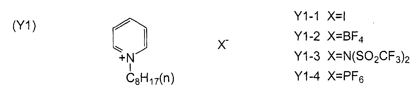
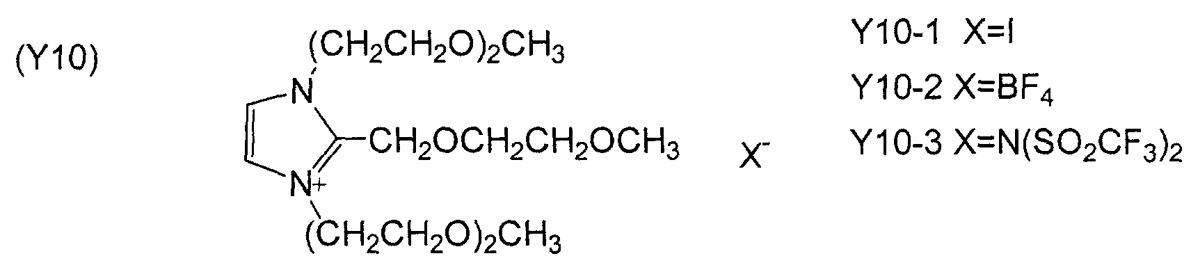
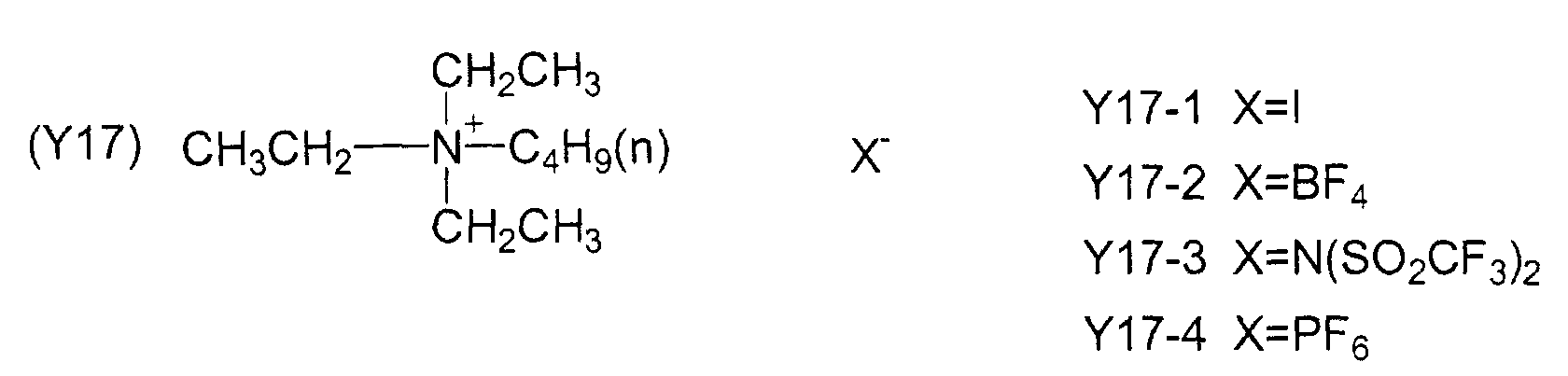
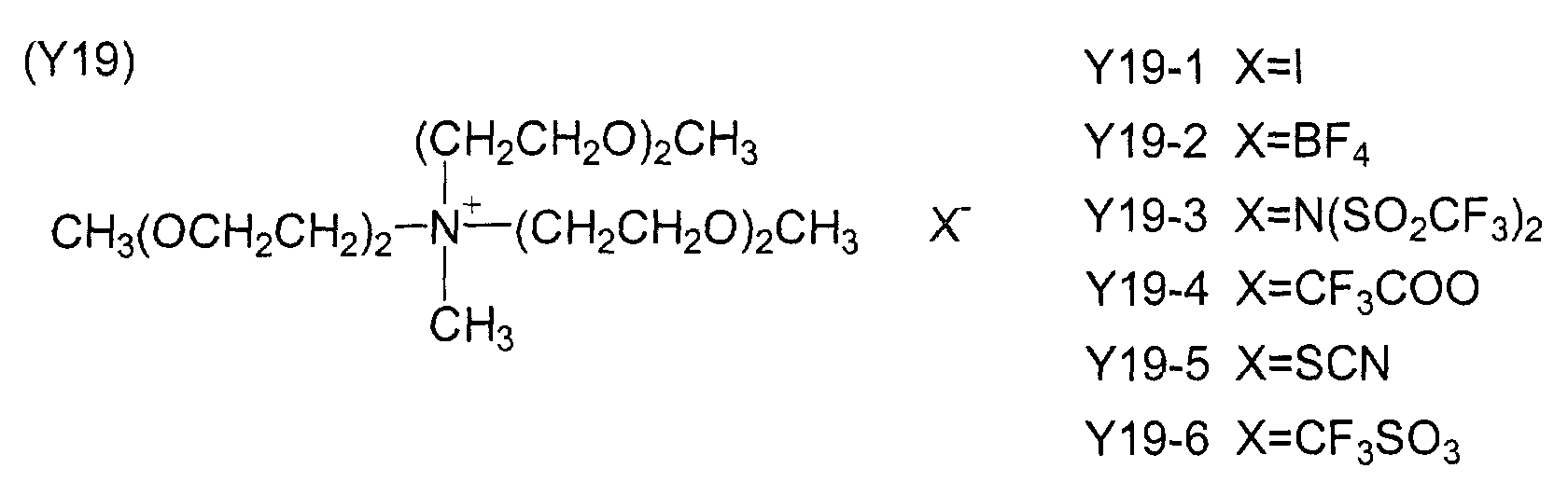
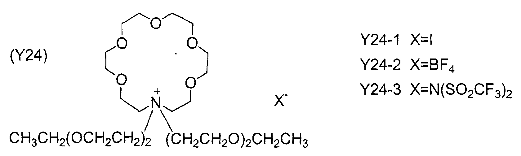
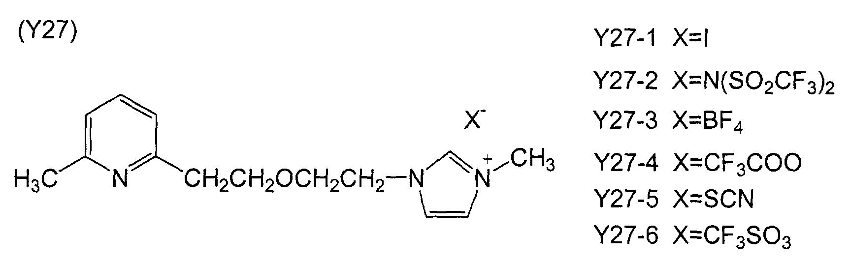
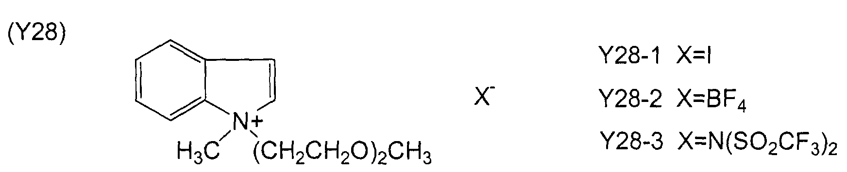
The molten salt electrolytes preferably used in the present invention will
be illustrated below without intention of restricting the scope of the present
invention defined by the claims attached hereto.
Though the molten salt electrolyte composition may comprise a solvent
described below, it particularly preferably comprises no solvent. The content of
the molten salt electrolyte is preferably 50 weight % or more, particularly
preferably 90 weight % or more, based on the entire composition. The weight
ratio of the iodine salts contained in the molten salt electrolyte composition is
preferably 50 weight % or more to the entire salts contained therein.
The molten salt electrolyte composition preferably comprises iodine.
The iodine-content is preferably 0.1 to 20 weight %, more preferably 0.5 to 5
weight % based on the entire composition.
(2) Electrolysis Solution
The electrolysis solution used in the present invention is preferably
composed of an electrolyte, a solvent and an additive. The electrolyte may be:
a combination of I2 and an iodide (a metal iodide such as LiI, NaI, KI, CsI and
CaI2, a quaternary ammonium iodide such as a tetralkylammonium iodide,
pyridinium iodide and imidazolium iodide, etc.); a combination of Br2 and a
bromide (a metal bromide such as LiBr, NaBr, KBr, CsBr and CaBr2, a
quaternary ammonium bromide such as a tetralkylammonium bromide and
pyridinium bromide, etc.); a metal complex such as a ferrocyanide-ferricyanide
and a ferrocene-ferricinium ion; a sulfur compound such as sodium polysulfide
and alkylthiol-alkyldisulfide; a viologen dye; hydroquinone-quinone; etc.
Among them, preferred is a combination of I2 and LiI or the quaternary
ammonium iodide. A plurality of the electrolytes may be mixed to be in use.
The concentration of the electrolyte in the electrolysis solution is
preferably 0.1 to 10 M, more preferably 0.2 to 4 M. Further, the electrolysis
solution may comprise iodine, and the concentration of iodine therein is
preferably 0.01 to 0.5 M.
The solvent used for the electrolysis solution is preferably such that has a
low viscosity and a high ionic mobility, or that has a high permittivity and can
increase the actual carrier concentration of the electrolysis solution, to exhibit an
excellent ionic conductibility. Examples of the solvent include: carbonates
such as ethylene carbonate and propylene carbonate; heterocyclic compounds
such as 3-methyl-2-oxazolidinone; ethers such as dioxan and diethyl ether; chain
ethers such as ethyleneglycol dialkylethers, propyleneglycol dialkylethers,
polyethyleneglycol dialkylethers and polypropyleneglycol dialkylethers;
alcohols such as methanol, ethanol, ethyleneglycol monoalkylethers,
propyleneglycol monoalkylethers, polyethyleneglycol monoalkylethers and
polypropyleneglycol monoalkylethers; glycols such as ethylene glycol,
propylene glycol, polyethylene glycol, polypropylene glycol and glycerin; nitrile
compounds such as acetonitrile, glutarodinitrile, methoxyacetonitrile,
propionitrile and benzonitrile; aprotic polar solvents such as dimethylsulfoxide
(DMSO) and sulfolane; water; etc. These solvents may be used in combination
with each other.
Further, to the above-mentioned molten salt electrolyte composition and
the electrolysis solution is preferably added a basic compound such as t-butylpyridine,
2-picoline, 2,6-lutidine, etc., as described in J. Am. Ceram. Soc.,
80 (12), 3157 to 3171 (1997). The concentration of the basic compound therein
is preferably 0.05 to 2 M.
(3) Gel Electrolyte Composition
The molten salt electrolyte composition and the electrolysis solution
mentioned above may be gelled (solidified) to prepare the gel electrolyte
composition. Gelation may be achieved by: adding a polymer; adding an oil-gelling
agent; polymerization of monomers including a multifunctional
monomer; a cross-linking reaction of a polymer; etc.
In the case where the gel electrolyte composition is prepared by adding a
polymer, compounds described in "Polymer Electrolyte Reviews 1 and 2", edited
by J. R. MacCallum and C. A. Vincent, ELSEIVER APPLIED SCIENCE may
be used as the polymer. Of the compounds, polyacrylonitrile and
poly(vinylidene fluoride) are preferred.
In the case where the gel electrolyte composition is prepared by adding
an oil-gelling agent, compounds described in J. Chem. Soc. Japan, Ind. Chem.
Soc., 46, 779 (1943), J. Am. Chem. Soc., 111, 5542 (1989), J. Chem. Soc.,
Chem. Commun., 390 (1993), Angew. Chem. Int. Ed. Engl., 35, 1949 (1996),
Chem. Lett., 885 (1996), J. Chem. Soc., Chem. Commun., 545 (1997), etc. may
be used as the oil-gelling agent. Of the compounds, preferred are those having
an amide structure.
In the case where the gel electrolyte composition is prepared by a cross-linking
reaction of a polymer, it is preferable that a polymer containing a group
having cross-linking reactivity is used in combination with a cross-linking agent.
The group having the cross-linking reactivity is preferably amino group or a
nitrogen-containing heterocyclic group such as pyridyl group, imidazolyl group,
thiazolyl group, oxazolyl group, triazolyl group, morpholyl group, piperidyl
group, piperazyl group, etc. The cross-linking agent is preferably an
electrophilic agent having a plurality of functional group that can be attacked by
the nitrogen atom, for example, multi-functional alkyl halides, aralkyl halides,
sulfonates, acid anhydrides, acyl chlorides, isocyanates, α,β-unsaturated
sulfonyl compounds, α,β-unsaturated carbonyl compounds, α,β-unsaturated
nitrile compounds, etc. Cross-linking methods disclosed in Japanese Patent
Laid-Open Nos. 2000-17076 and 2000-86724 may be used in the present
invention.
Further, a method for gelling an electrolysis solution disclosed in
Japanese Patent Laid-Open No. 11-185863 and a method for gelling a molten
salt electrolyte composition disclosed in Japanese Patent Laid-Open No. 2000-58140
may be used in this invention.
(4) Hole-Transporting Material
In the present invention, an organic solid hole-transporting material, an
inorganic solid hole-transporting material or a combination thereof may be used
for the charge transfer layer instead of the ion conductive electrolyte
composition such as the molten salt electrolyte composition.
(a) Organic Hole-Transporting Material
Preferred examples of the organic hole-transporting material used in this
invention include: aromatic amines disclosed in J. Hagen, et al., Synthetic Metal,
89, 215 to 220 (1997), Nature, Vol. 395, 8 Oct. 1998, Page 583 to 585, WO
97/10617, United States Patent Nos. 4,923,774 and 4,764,625, Japanese Patent
Laid-Open Nos. 59-194393, 5-234681, 4-308688, 3-269084, 4-129271, 4-175395,
4-264189, 4-290851, 4-364153, 5-25473, 5-239455, 5-320634, 6-1972,
7-138562, 7-252474 and 11-144773, etc.; triphenylenes disclosed in Japanese
Patent Laid-Open Nos. 11-149821, 11-148067 and 11-176489, etc.;
oligothiophene compounds disclosed in Adv. Mater., 9, No. 7, 557, 1997,
Angew. Chem. Int. Ed. Engl., 34, 3, 303 to 307, 1995, J. Am. Chem. Soc., Vol.
120, No. 4, Page 664 to 672, 1998, etc.; and conductive polymers such as
polypyrrole disclosed in K. Murakoshi, et al., Chem. Lett., 471, 1997 and
polyacetylene, poly(p-phenylene), poly(p-phenylenevinylene),
polythienylenevinylene, polythiophene, polyaniline, polytoluidine and
derivatives thereof disclosed in "Handbook of Organic Conductive Molecules
and Polymers", Vol. 1 to 4, edited by NALWA, published by WILEY.
As described in Nature, Vol. 395, 8 Oct. 583 to 585 (1998), to the
organic hole-transporting material may be added a compound having cation
radical such as tris(4-bromophenyl)aminium hexachloroantimonate to control
the dopant level, or a salt such as Li[(CF3SO2)2N] to achieve potential-control of
surface of the semiconductor, thereby compensating a space-charge layer.
(b) Inorganic Hole-Transporting Material
The inorganic hole-transporting material may be a p-type inorganic
compound semiconductor. Band gap of the p-type inorganic compound
semiconductor is preferably 2 eV or more, more preferably 2.5 eV or more.
Ionization potential of the p-type inorganic compound semiconductor should be
smaller than that of the photosensitive layer to reduce holes of the dye.
Although the ionization potential of the p-type inorganic compound
semiconductor may be selected depending on the kind of the dye, generally, it is
preferably 4.5 to 5.5 eV, more preferably 4.7 to 5.3 eV. The p-type inorganic
compound semiconductor is preferably a compound having a monovalent
copper such as CuI, CuSCN, CuInSe2, Cu(In,Ga)Se2, CuGaSe2, Cu2O, CuS,
CuGaS2, CuInS2, CuAlSe2, etc. Among them, CuI and CuSCN are preferred,
and CuI is the most preferred. GaP, NiO, CoO, FeO, Bi2O3, MoO2, Cr2O3, etc.
are also used as the p-type inorganic compound semiconductor.
(5) Method for Forming Charge Transfer Layer
The charge transfer layer may be provided by any of the following two
methods. One is a method where the counter electrode is stuck on the
photosensitive layer beforehand and the material for the charge transfer layer in
the liquid state is made to penetrate a gap therebetween. Another is a method
where the charge transfer layer is directly disposed on the photosensitive layer,
the counter electrode being then disposed thereon.
In the former method, the material for the charge transfer layer may be
made to penetrate the gap by a normal pressure process utilizing capillarity, or
by a reduced pressure process where the material is pumped up from the gap to
replace gas phase therein with liquid phase.
In the case of providing a wet charge transfer layer by the latter method,
the wet charge transfer layer is applied to the photosensitive layer, the counter
electrode is disposed on the wet charge transfer layer without drying it, and edges
thereof is subjected to a treatment for preventing liquid-leakage, if necessary.
In the case of providing a gel charge transfer layer by the latter method, the
charge transfer material may be applied in the liquid state and gelled by
polymerization, etc. In this case, the counter electrode may be disposed on the
charge transfer layer before or after drying and fixing the charge transfer layer.
The charge transfer layer composed of the electrolysis solution, the wet
organic hole-transporting material, the gel electrolyte composition, etc. may be
disposed by a soaking method, a roller method, a dip method, an air-knife
method, an extrusion method, a slide-hopper method, a wire-bar method, a spin
method, a spray method, a cast method, various printing methods, etc. similarly
to the case of forming the semiconductor fine particle layer, or adsorbing a dye
to the semiconductor mentioned above.
The charge transfer layer composed of the solid electrolyte, the solid hole
transporting material, etc. may be formed by a dry film-forming method such as
a vacuum deposition method and a CVD method, and followed by disposing the
counter electrode thereon. The organic hole-transporting material may be
made to penetrate into the photosensitive layer by a vacuum deposition method,
a cast method, a coating method, a spin-coating method, a soaking method, an
electrolytic polymerization method, a photo-polymerization method, etc. The
inorganic hole-transporting material may be made to penetrate into the
photosensitive layer by a cast method, a coating method, a spin-coating method,
a soaking method, an electrolytic deposition method, an electroless deposition
method, etc.
(E) Counter Electrode
The counter electrode is the counter electrically conductive layer, which
is supported by the substrate, if necessary. Examples of the electrically
conductive material used for the counter electrically conductive layer include:
metals such as platinum, gold, silver, copper, aluminum, magnesium, rhodium
and indium; carbon; and electrically conductive metal oxides such as indium-tin
composite oxides and fluorine-doped tin oxides. Among them, preferred are
platinum, gold, silver, copper, aluminum and magnesium. The substrate of the
counter electrode is preferably made of a glass or a plastic, to be coated or
vapor-deposited with the electrically conductive material. The counter
electrically conductive layer preferably has a thickness of 3 nm to 10 µm,
although the thickness is not particularly limited. The surface resistance of the
counter electrically conductive layer is desirably as low as possible. The
surface resistance is preferably 50 Ω/square or less, more preferably 20 Ω/square
or less.
Light may be irradiated from any one or both side of the conductive
support and the counter electrode, so that at least one of them must be
substantially transparent to have light reached to the photosensitive layer.
From a viewpoint of improving electric generation efficiency, it is preferable that
the conductive support is transparent to irradiate light therethrough. In this
case, the counter electrode preferably has a light-reflective property. Such a
counter electrode may be composed of a glass or a plastic having a vapor-deposited
layer of metal or electrically conductive oxide, or metal thin film.
The counter electrode may be disposed by applying, metal-plating, or
vapor-depositing (PVD, CVD, etc.) the electrically conductive material directly
on the charge transfer layer. Alternatively, the counter electrode composed of
the substrate and the counter electrically conductive layer may be disposed by
sticking the counter electrically conductive layer side surface thereof on the
charge transfer layer. Further, the counter electrode may be disposed on the
photosensitive layer through a spacer before forming the charge transfer layer.
It is preferable that the metal lead is used to reduce the resistance of the counter
electrode, as is similar to the conductive support. The metal lead is particularly
preferably used for the transparent counter electrode. Preferable embodiments
of the metal lead used for the counter electrode are the same as those of the
metal lead used for the conductive support mentioned above.
(F) Others
It is preferable that a fine semiconductor thin film is provided between
the conductive support and the photosensitive layer as an undercoating layer to
prevent short-circuit of the counter electrode and the conductive support,
particularly in the case of the charge transfer layer composed of the electron-transporting
material or the hole-transporting material. The undercoating layer
is preferably made of TiO2, SnO2, Fe2O3, WO3, ZnO or Nb2O5, more preferably
made of TiO2. The undercoating layer may be disposed by a spray-pyrolysis
method described in Electrochim. Acta, 40, 643 to 652 (1995), a sputtering
method, etc. The thickness of the undercoating layer is preferably 5 to 1000
nm, more preferably 10 to 500 nm.
Functional layers such as a protective layer and a reflection-preventing
layer may be disposed on any one or both of the conductive support and the
counter electrode. The functional layers may be disposed by a method selected
in accordance with the materials therefor, such as a coating method, a vapor-deposition
method and a sticking method.
(G) Interior Structure of Photoelectric Conversion Device
As described above, the photoelectric conversion device may have
various interior structures in accordance with an end of use. The structures are
classified into two major forms, a structure allowing light incidence from both
faces, and a structure allowing it from only one face. Each of Figs. 2 to 9
illustrates an example of the interior structure of the photoelectric conversion
device, which is preferable in the present invention.
As for the structure illustrated in Fig. 2, the photosensitive layer 20 and
the charge transfer layer 30 are disposed between the transparent electrically
conductive layer 10a and the transparent counter electrically conductive layer
40a. This structure allows light incidence from both faces of the device.
As for the structure illustrated in Fig. 3, on the transparent substrate 50a
partially having the metal lead 11 is disposed the transparent electrically
conductive layer 10a, the undercoating layer 60, the photosensitive layer 20, the
charge transfer layer 30 and the counter electrically conductive layer 40 are
laminated in this order, and the substrate 50 is further placed thereon. This
structure allows light incidence from the electrically conductive layer side.
As for the structure illustrated in Fig. 4, the photosensitive layer 20 is
disposed on the substrate 50 having the electrically conductive layer 10 through
the undercoating layer 60, the charge transfer layer 30 and the transparent
counter electrically conductive layer 40a are disposed thereon, and further the
transparent substrate 50a locally having the metal lead 11 is placed on the
counter electrically conductive layer 40a so that the metal lead 11 side orients
inward. This structure allows light incidence from the counter electrode side.
As for the structure illustrated in Fig. 5, on the two transparent substrates
50a each having the metal lead 11 partially are formed the transparent
electrically conductive layer 10a and the transparent counter electrically
conductive layer 40a, respectively, and the undercoating layer 60, the
photosensitive layer 20 and the charge transfer layer 30 placed between the
conductive layers. This structure allows light incidence from both faces of the
photoelectric conversion device.
As for the structure illustrated in Fig. 6, on the transparent substrate 50a
having the transparent electrically conductive layer 10a is disposed the
photosensitive layer 20 through the undercoating layer 60, the charge transfer
layer 30 and the counter electrically conductive layer 40 are formed thereon, and
further the substrate 50 is placed on the counter electrically conductive layer 40.
This structure allows light incidence from the electrically conductive layer side.
As for the structure illustrated in Fig. 7, on the substrate 50 having the
electrically conductive layer 10 is disposed the photosensitive layer 20 through
the undercoating layer 60, the charge transfer layer 30 and the transparent
counter electrically conductive layer 40a are formed thereon, and further the
transparent substrate 50a is placed on the layer 40a. This structure allows light
incidence from the counter electrode side.
As for the structure illustrated in Fig. 8, on the transparent substrate 50a
having the transparent electrically conductive layer 10a is disposed the
photosensitive layer 20 through the undercoating layer 60, the charge transfer
layer 30 and the transparent counter electrically conductive layer 40a are formed
thereon, and further the transparent substrate 50a is placed on the layer 40a.
This structure allows light incidence from both faces of the photoelectric
conversion device.
As for the structure illustrated in Fig. 9, the photosensitive layer 20 is
disposed on the substrate 50 having the electrically conductive layer 10 through
the undercoating layer 60, the solid charge transfer layer 30 is disposed thereon,
and further the counter electrically conductive layer 40 or the metal lead 11 is
locally placed on the solid charge transfer layer 30. This structure allows light
incidence from the counter electrode side.
[2] Photoelectric Cell
The photoelectric cell of the present invention is constituted by
connecting the photoelectric conversion device of the present invention to an
external circuit to electrically work or generate electricity in the external circuit.
Such a photoelectric cell that has the charge transfer layer composed of ion
conductive electrolyte composition is referred to as a photo-electrochemical cell.
A photoelectric cell intended for power generation using solar light is referred to
as a solar cell.
The side face of the photoelectric cell is preferably sealed with a polymer
or an adhesive agent, etc. to prevent deterioration and volatility of the content in
the cell. The external circuit is connected to the conductive support and the
counter electrode via a lead. Various known circuits may be used in the
present invention.
In the case where the photoelectric conversion device of the present
invention is applied to the solar cell, the interior structure of the solar cell may
be essentially the same as that of the photoelectric conversion device mentioned
above. The solar cell comprising the photoelectric conversion device of the
present invention may have a known module structure. In general module
structure of the solar cell, cells are placed on a substrate of metal, ceramic, etc.
and covered with a packing resin, a protective glass, etc., whereby light is
introduced from the opposite side of the substrate. The solar cell module may
have a structure where the cells are placed on a substrate of a transparent
material such as a tempered glass to introduce light from the transparent
substrate side. Specifically, a superstraight type module structure, a substrate
type module structure, a potting type module structure, substrate-integrated type
module structure that is generally used in amorphous silicon solar cells, etc. are
known as the solar cell module structure. The solar cell comprising the
photoelectric conversion device of the present invention may have a module
structure properly selected from the above structures in accordance with ends
and environment at use, and preferably has a module structure disclosed in
Japanese Patent Laid-Open No. 11-8457.
EXAMPLES
The present invention will be explained in more detail with reference to
examples below without intention of restricting the scope of the present
invention.
1. Preparation of Coating Dispersion Containing Titanium Dioxide
A titanium dioxide dispersion was prepared in the same manner as a
method disclosed in C. J. Barbe, et al, J. Am. Ceramic Soc., 80, 3157 except that
the autoclave temperature was 230 °C. The weight ratio of titanium dioxide
fine particles was 11 weight % and the average diameter thereof was
approximately 10 nm in the titanium dioxide dispersion. Then, 20 weight % of
polyethylene glycol (average molecular weight: 20000, Wako Pure Chemical
Industries, Ltd.) was added to 100 weight % of the titanium dioxide dispersion,
and mixed to prepare a coating dispersion containing titanium dioxide.
2. Preparation of Dye-Adsorbed Titanium Dioxide Electrode
The above coating dispersion was applied onto an electrically conductive
surface of a transparent conductive support into a thickness of 130 µm by a
doctor blade, dried at 25 °C for 30 minutes, and baked by an electric furnace
"muffle furnace FP-32" manufactured by Yamato Science K.K. at 550 °C for 30
minutes to provide a titanium dioxide electrode having a titanium dioxide layer.
Used as the transparent conductive support was a conductive glass manufactured
by Nippon Sheet Glass Co., Ltd. having a surface resistance of approximately 10
Ω/cm2, which was composed of a glass substrate and an electrically conductive
layer of fluorine-doped tin oxide. Amount of the titanium dioxide in the
resultant titanium dioxide layer was 19 g/m2, and thickness of the titanium
dioxide layer was 13 µm.
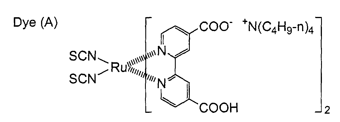
Thus-obtained titanium dioxide electrode was cooled, and soaked in a
dye adsorption solution
E-1 composed of a dye (A) shown below and a mixture
solvent of ethanol/
t-butanol/acetonitrile = 1/1/2 at an adsorbing temperature of
45 °C for an adsorbing period of 10 hours, to adsorb the dye (A) on the titanium
dioxide electrode. Concentration of the dye (A) in the dye adsorption solution
E-1 was 3 × 10
-3 mol/l. Then, the resultant electrode was washed with each of
ethanol and acetonitrile in this order, soaked in a treatment solution composed of
the quaternary salt (12) and acetonitrile at a treatment temperature of 40 °C for a
treatment period of 2 hours, washed with each of ethanol and acetonitrile in this
order, and dried in the dark under nitrogen gas stream, to prepare a dye-adsorbed
titanium dioxide electrode. Concentration of the quaternary salt (12) in the
treatment solution was 0.01 mol/l.
The 2 cm x 2 cm in size of the dye-adsorbed titanium dioxide electrode
was put on a platinum-deposited glass having the same size thereas. Then, an
electrolyte composition composed of 1,3-dimethylimidazolium iodide (0.65
mol/l), iodine (0.05 mol/l), t-butylpyridine (0.1 mol/l) and acetonitrile was
permeated into a crevice between the dye-adsorbed titanium dioxide electrode
and the platinum-deposited glass through capillarity, to produce a photoelectric
cell of Example 1.
Photoelectric cells of Examples 2 to 7 were produced in the same manner
as the photoelectric cell of Example 1 except that quaternary salts shown in
Table 2 were used for the treatment solution instead of the quaternary salt (12),
respectively. Incidentally, in the photoelectric cell of Example 7, 5 volume %
of t-butylpyridine was added to the treatment solution. Further, a photoelectric
cell of Comparative Example 1 was produced in the same manner as the
photoelectric cell of Example 1 except for not using the quaternary salt (12).
Furthermore, photoelectric cells of Examples 8 to 17 and Comparative
Examples 2 to 4 were produced in the same manner as the photoelectric cell of
Example 1 except for: that the coating dispersion was applied onto the
electrically conductive surface into a thickness of 120 µm and baked at 450 °C
after drying, and amount of the titanium dioxide in the titanium dioxide layer
was 18 g/m
2, and thickness of the titanium dioxide layer was 12 µm; that dye
adsorption solutions
E-2 to
E-4 shown in Table 1 were used instead of the dye
adsorption solution
E-1, the adsorbing temperature was 25 °C and the adsorbing
period was 16 hours; that treatment solutions shown in Table 2 were used
instead of the treatment solution composed of the quaternary salt (12), the
treatment temperature was 25 °C and the treatment period was 16 hours; and
t-butylpyridine
was not used for the electrolyte composition, respectively.
| Dye Adsorption Solution | Composition | Adsorbing Temperature (°C) | Adsorbing Period (hr) |
| | Dye | Solvent (Volume Ratio of Ethanol/t-Butanol/Acetonitrile) | Concentration of Dye (mol/l) |
| E-1 | (A) | 1/1/2 | 3 × 10⁻³ | 45 | 10 |
| E-2 | R-1 | 1/0/1 | 3 × 10⁻⁴ | 25 | 16 |
| E-3 | M-5 | 1/0/1 | 1 × 10⁴ | 25 | 16 |
| E-4 | M-4 | 1/0/1 | 1 × 10⁻⁴ | 25 | 16 |
A silver paste was applied to edge portion of the transparent conductive
support of each photoelectric cells of Examples 1 to 17 and Comparative
Examples 1 to 4, to form a negative electrode. Then, the negative electrode
and the platinum-deposited glass were connected to the current-voltage tester
"Keithley SMU238". Each of the resultant photoelectric cells was measured
with respect to current-voltage properties while perpendicularly irradiating a
simulated sunlight thereto, to obtain the photoelectric conversion efficiency.
The results were shown in Table 2. Herein, the simulated sunlight was
generated by passing the light of 500 W xenone lamp manufactured by Ushio
K.K. through "AM 1.5 filter" manufactured by Oriel Co, and had intensity of 100
mW/cm
2.
| Ex. No. | Dye Adsorption Solution | Treatment Solution | Treatment Temperature (°C) | Treatment Period (hr) | Photoelectric Conversion Efficiency (%) |
| | | Quaternary Salt | Solvent | Concentration of Quaternary Salt (mol/l) |
| Ex. 1 | E-1 | (12) | Acetonitrile | 0.01 | 40 | 2 | 5.7 |
| Ex. 2 | E-1 | (13) | Acetonitrile | 0.01 | 40 | 2 | 6.5 |
| Ex. 3 | E-1 | (14) | Acetonitrile | 0.01 | 40 | 2 | 7.2 |
| Ex. 4 | E-1 | (15) | Acetonitrile | 0.01 | 40 | 2 | 7.5 |
| Ex. 5 | E-1 | (16) | Acetonitrile | 0.01 | 40 | 2 | 7.3 |
| Ex. 6 | E-1 | (17) | Acetonitrile | 0.01 | 40 | 2 | 5.8 |
| Ex. 7 | E-1 | (15) | Acetonitrile | 0.01 | 40 | 2 | 7.7 |
| Comp. Ex. 1 | E-1 | None | Acetonitrile | ― | 40 | 2 | 4.9 |
| Ex.8 | E-2 | (28) | Acetonitrile | 0.04 | 25 | 16 | 6.7 |
| Ex. 9 | E-2 | (27) | Acetonitrile | 0.04 | 25 | 16 | 6.0 |
| Ex. 10 | E-2 | (29) | Acetonitrile | 0.04 | 25 | 16 | 6.5 |
| Ex. 11 | E-2 | (34) | Acetonitrile | 0.04 | 25 | 16 | 7.1 |
| Ex. 12 | E-2 | (35) | Acetonitrile | 0.04 | 25 | 16 | 7.0 |
| Ex. 13 | E-2 | (38) | Acetonitrile | 0.04 | 25 | 16 | 6.9 |
| Ex. 14 | E-2 | (39) | Acetonitrile | 0.04 | 25 | 16 | 5.9 |
| Ex. 15 | E-2 | (46) | Acetonitrile | 0.04 | 25 | 16 | 7.2 |
| Comp. Ex. 2 | E-2 | None | Acetonitrile | ― | 25 | 16 | 5.5 |
| Ex. 16 | E-3 | (28) | Acetonitrile | 0.04 | 25 | 16 | 4.4 |
| Comp. Ex. 3 | E-3 | None | Acetonitrile | ― | 25 | 16 | 3.8 |
| Ex. 17 | E-4 | (28) | Acetonitrile | 0.04 | 25 | 16 | 4.2 |
| Comp. Ex. 4 | E-4 | None | Acetonitrile | ― | 25 | 16 | 3.5 |
Comparing Examples 1 to 7 with Comparative Example 1, Examples 8
to 15 with Comparative Example 2, Example 16 with Comparative Example 3,
and Example 17 with Comparative Example 4, the photoelectric cells of the
present invention using the dye treated with the quaternary salt exhibited high
photoelectric conversion efficiency not depending on the kind of the dye.
As compared with the photoelectric cells of Examples 1 and 6, the
photoelectric cell of Example 2 exhibited higher photoelectric conversion
efficiency. It was clear from this that the tetralkylammonium salt was
preferably used as the quaternary salt. Further, the photoelectric cells of
Examples 3 to 5 exhibited the photoelectric conversion efficiency higher than
that of the photoelectric cell of Example 2, accordingly, it was preferred that the
tetralkylammonium salt has an alkyl group containing 6 or more carbon atoms
such as a hexyl group.
Among Examples 1 to 17, the photoelectric cell of Example 7 exhibited
the most excellent photoelectric conversion efficiency. This seemed because
the preferred quaternary salt was used in combination with a pyridine
compound.
As described in detail above, a photoelectric conversion device of the
present invention is excellent in photoelectric conversion efficiency. Thus, a
photoelectric cell of the present invention using this photoelectric conversion
device is remarkably usable as a solar cell.