EP1162748A1 - Dispositif et procédé de contrôle de condensateurs intégrés - Google Patents
Dispositif et procédé de contrôle de condensateurs intégrés Download PDFInfo
- Publication number
- EP1162748A1 EP1162748A1 EP01401421A EP01401421A EP1162748A1 EP 1162748 A1 EP1162748 A1 EP 1162748A1 EP 01401421 A EP01401421 A EP 01401421A EP 01401421 A EP01401421 A EP 01401421A EP 1162748 A1 EP1162748 A1 EP 1162748A1
- Authority
- EP
- European Patent Office
- Prior art keywords
- node
- capacitors
- capacitive structure
- ground
- integrated
- Prior art date
- Legal status (The legal status is an assumption and is not a legal conclusion. Google has not performed a legal analysis and makes no representation as to the accuracy of the status listed.)
- Granted
Links
- 239000003990 capacitor Substances 0.000 title abstract description 77
- 238000000034 method Methods 0.000 title abstract description 10
- 239000004065 semiconductor Substances 0.000 abstract description 7
- 238000005259 measurement Methods 0.000 description 23
- 238000004519 manufacturing process Methods 0.000 description 7
- 230000007547 defect Effects 0.000 description 5
- 230000002787 reinforcement Effects 0.000 description 5
- 235000021183 entrée Nutrition 0.000 description 3
- 230000003071 parasitic effect Effects 0.000 description 3
- XUIMIQQOPSSXEZ-UHFFFAOYSA-N Silicon Chemical compound [Si] XUIMIQQOPSSXEZ-UHFFFAOYSA-N 0.000 description 2
- 244000045947 parasite Species 0.000 description 2
- 239000008188 pellet Substances 0.000 description 2
- 230000035945 sensitivity Effects 0.000 description 2
- 229910052710 silicon Inorganic materials 0.000 description 2
- 239000010703 silicon Substances 0.000 description 2
- 239000000243 solution Substances 0.000 description 2
- 238000012512 characterization method Methods 0.000 description 1
- 238000006243 chemical reaction Methods 0.000 description 1
- 230000001186 cumulative effect Effects 0.000 description 1
- 230000001419 dependent effect Effects 0.000 description 1
- 238000010586 diagram Methods 0.000 description 1
- 230000000694 effects Effects 0.000 description 1
- 230000008030 elimination Effects 0.000 description 1
- 238000003379 elimination reaction Methods 0.000 description 1
- 238000002347 injection Methods 0.000 description 1
- 239000007924 injection Substances 0.000 description 1
- 230000010354 integration Effects 0.000 description 1
- 238000003908 quality control method Methods 0.000 description 1
- 230000003014 reinforcing effect Effects 0.000 description 1
- 239000000758 substrate Substances 0.000 description 1
- 238000011144 upstream manufacturing Methods 0.000 description 1
Images


Classifications
-
- H—ELECTRICITY
- H03—ELECTRONIC CIRCUITRY
- H03M—CODING; DECODING; CODE CONVERSION IN GENERAL
- H03M1/00—Analogue/digital conversion; Digital/analogue conversion
- H03M1/10—Calibration or testing
- H03M1/1071—Measuring or testing
- H03M1/109—Measuring or testing for DC performance, i.e. static testing
-
- H—ELECTRICITY
- H03—ELECTRONIC CIRCUITRY
- H03M—CODING; DECODING; CODE CONVERSION IN GENERAL
- H03M1/00—Analogue/digital conversion; Digital/analogue conversion
- H03M1/66—Digital/analogue converters
- H03M1/74—Simultaneous conversion
- H03M1/78—Simultaneous conversion using ladder network
Definitions
- the invention relates to integrated circuits, and more particularly the control of integrated capacitors, such as the control of matching ("matching" in English) and the linearity of these integrated capacitors.
- the invention applies advantageously but not exclusively for quality control of circuit capacitors integrated in production. It also finds an application in the field of analog-to-digital converters operating on the principle of switched capacities.
- An integrated circuit comprising for example a converter analog digital to switched capacities, can include in theory a certain number of identical capacitors in terms of values capacitive.
- these theoretically identical capacitors have practice slightly different actual characteristics. These real characteristics result in particular in faults matching, that is, there are differences between their values respective actual capacitives.
- These mismatches are caused by example to slightly different reinforcement surfaces of a capacitor to the other or to differences in permittivity of dielectric from one capacitor to another. The causes of these differences are generally linked to the inevitable vagaries of the manufacturing process (non-uniform deposited oxide quality, use of plasma, location of the capacitors on the plate, ).
- the invention aims to remedy this shortcoming.
- the invention aims to provide a simple control of control of capacitors produced.
- Another object of the invention is to propose a system allowing to determine at the same time the lack of pairing and the non-linearity theoretically identical integrated capacitors, using of a single decisional parameter which is similar to a resolution in number of bits.
- the invention also aims to use this system for very quickly and very effectively check the mismatch and the non-linearity of theoretically identical capacitors belonging to integrated circuits produced in production on a semiconductor wafer.
- Another object of the invention is to very simply determine the actual maximum resolution of analog-to-digital converters made on integrated circuits.
- the invention also aims to provide a generator reference voltages for analog-to-digital converters which is particularly robust and precise.
- the invention therefore provides a device for controlling theoretically identical integrated capacitors, this device comprising a capacitive structure having an input node and n output nodes, n being an integer greater than or equal to 2.
- the capacitive structure also has r capacitors integrated connected in series between two neighboring nodes, r being an integer greater than or equal to 1.
- This capacitive structure still has 1 integrated capacitor connected between the input node and ground and 1 integrated capacitor connected between the n th output node and the mass.
- This capacitive structure also has r capacitive branches connected in parallel between the ground and each node of the capacitive structure including the first output node and the n-1 th output node. Each branch has r + 1 integrated capacitors connected in series. All the capacitors of the capacitive structure are theoretically identical.
- the charging means comprise a reference voltage source and a controllable switch connected between the voltage source and the input node.
- the measurement means comprise for each node of the capacitive structure, a switch control unit connected to said node, and an ammeter capable of be connected between the measurement switch and earth.
- Using an ammeter to measure a charge in each of the nodes of the capacitive structure is particularly advantageous compared to a solution consisting in measuring voltages across the capacitors because a voltmeter has capacities parasites, which can distort the measurement.
- the device also advantageously comprises, for each node of the capacitive structure, a controllable switch of discharge connected between said node and ground. This allows to unload all capacitors before measurement.
- the device according to the invention is advantageously used for control of integrated capacitors belonging to an integrated circuit located on a wafer of a semiconductor wafer and delimited by cutting paths provided in said wafer.
- the structure capacitive is then advantageously inserted in one of the paths of cut-out defining said patch and the reinforcing surface of capacitors of the capacitive structure is then chosen at most equal to the minimum armature area of the integrated circuit capacitors.
- the integrated circuit comprises capacitors with the same armature area
- the integrated circuit includes capacitors having different reinforcement surfaces, for example a group of capacitors having a first predetermined armature surface, and another group of capacitors having a second armature surface equal to half of the first reinforcement area, we will then choose a capacitive structure whose capacitors have a surface reinforcement equal to the second reinforcement surface.
- the capacitive structure of the device according to the invention can also be used as a generator of voltages or loads of benchmark for a capacity analog-to-digital converter switched.
- a voltage source is connected to the node entry.
- the different reference voltages or loads are then respectively available at the level of the different nodes (which are output nodes) of the capacitive structure.
- the frequency should be high enough to allow the ammeter to average and deliver current sufficiently large, therefore capable of being measured with good accuracy. However, this frequency should not be too high to avoid injecting charges into the switches, causing phenomena parasites.
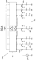
- the reference DCA designates a control device according to the invention.
- This control device comprises a capacitive structure SCA having an input node ND 0 and n output nodes ND 1 -ND n .
- n is an integer greater than or equal to 2.
- the capacitive structure also includes an integrated capacitor C connected in series between two neighboring nodes ND i and ND i + 1 .
- the capacitive structure also comprises a capacitive branch BR i connected between ground and each node ND i of the capacitive structure, including the first output node ND 1 and the n-1 th output node ND n-1 .
- the capacitive structure CA comprises n-1 capacitive branches BR 1 -BR n-1 respectively connected to the nodes ND 1 -ND n-1 .
- Each capacitive branch BR i has two integrated capacitors C connected in series.
- All the capacitors C of the capacitive structure are theoretically identical. In practice, they are carried out in an integrated manner within a semiconductor substrate.
- the capacitors the capacitive structure and the capacitors of the integrated circuits are performed simultaneously according to the same manufacturing process.
- the DCA control device comprises, in addition to the capacitive structure SCA, charging means MCH able to charge each node of the capacitive structure.
- charging means MCH here comprise a reference voltage source STR delivering a reference voltage V to the input node ND 0 by means of a controllable switch Sv.
- the DCA device further comprises measurement means capable of measuring the load at each of the nodes of the capacitive structure.
- measurement means here comprise, for each node of the capacitive structure, a controllable measurement switch S i connected to the node ND i , as well as an ammeter Amp connected between the measurement switch S i and the ground.
- a controllable discharge switch S res connected between the node ND i and the ground.
- the reference C p designates capacitors representative of the parasitic capacitances of the system.
- the SCA capacitive structure according to the invention has remarkable properties, namely a node tension division at node and a constant capacitive value at each node.
- the voltage at each node of the SCA structure is divided by two compared to the voltage at the upstream node. If one refers to the voltage V of the reference voltage source STR, the voltage V i at each node ND i of the structure SCA is equal to V / 2 i .
- the capacitive value at each node ND i is constant and is equal to 3C / 2.
- the invention advantageously provides for measuring the charge Q i at each node ND i of the capacitive structure so as to obtain a value representative of the voltage V i without parasitic capacity in the measurement chain.
- a particularly simple and effective way of measuring this charge consists in measuring the current I i in each node using the ammeter Amp.
- FIG. 2 We now refer more particularly to FIG. 2, for describe in more detail such a mode of implementation.
- the charge Q i or even the current I i , will successively be calculated in each of the nodes ND i with i varying from 0 to n.
- step 23 all the nodes are discharged, and consequently the node considered, by closing and opening the switch S res successively.
- step 24 the switch S v is firstly closed for a predetermined duration, so as to load the nodes of the structure SCA.
- the switch S v can be left closed for 100 ns.
- the switch S v is then opened so as to allow subsequent reading.
- the switch S i is closed in step 25 then, after a predetermined measurement time, this switch S i is opened again in step 26.
- step 27 After incrementing the counter j by one unit (step 27), we repeats the cycle of steps 23 to 27 until the counter j reaches a predetermined final value J corresponding to a duration predetermined measurement.
- the duration of a charge and measurement discharge cycle (steps 23 to 26) is of the order of 1 ms corresponding to a frequency f of 1 MHz.
- the number J is chosen so as to have an integration of the measurement over a duration of the order of a second, for example of the order of 3 seconds.
- the frequency f must be high enough to allow an accurate reading of the current with a sufficiently large current value, for example of the order of 1 mA, but not too high to avoid the appearance of parasitic phenomena. due in particular to the injection of charges into the switches.
- a capacitor C having a capacitive value of 1 pF, a frequency between 100 KHz and 10 MHz.
- step 29 the counter i is incremented by one unit (step 29), and the discharge, charge and measurement algorithm is re-executed until all the nodes of the capacitive structure have been considered (step 31).
- the ratio of real currents I i and I 0 is defined by formula (3) and can be analyzed as the sum of a theoretical value TH i ⁇ a tolerance TL i, x .
- step (30) of each measured nodal load value with a theoretical nodal load value results here in the comparison of a current ratio with respect to a theoretical value TH i , taking into account a predetermined tolerance TL i, x .
- This quality coefficient CQx is in fact the index i of the last node ND i whose current I i satisfies formula (3), that is to say whose current I i is within the fixed tolerance range.
- a capacitive structure having the quality coefficient 4 will have less linearity defect and better matching than a capacitive structure having obtained the quality coefficient 2.
- the integer x in formula (3) can take values greater than or equal to 1.
- the tolerance criterion defined by formula (3) is more sensitive to faults in linearity than to faults in pairing.
- an equal sensitivity for the linearity defects and for the mismatches is obtained with the cumulative criterion defined by the formula (4) below: in which i denotes the index of the node considered.
- the integer x in formula (4) increases the sensitivity of a SCA capacitive structure for a value of "n" fixed and given.
- n the quality coefficient CQ1 obtained for x equal to 1
- the fact of using a value of x equal to 2 for example would virtually expand the characterization limit of the SCA structure, and to obtain a CQ2 quality criterion of less than 20 corresponding to a greater constraint.
- the SCA capacitive structure can be used for different applications. It can be used to test, for example, processes different manufacturing of capacitors, so as to use the process which will minimize the linearity and matching defects in the capacitors.
- the SCA structure also makes it possible to characterize very simply the actual maximum resolution of an analog-to-digital converter with switched capacities.
- the quality coefficient that we mentioned above i.e. the number corresponding to the index of last node of the structure having satisfied the criterion defined by the formula (3) in particular or by the formula (4) for example, in fact corresponds to a number of bits representative of the maximum resolution of the converter analog-digital with switched capacities.
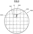
- the invention also makes it possible to control the fault of matching and linearity of integrated circuit capacitors or else the actual maximum resolution of analog-to-digital converters with switched capacities, by realizing this capacitive structure in cutting paths of a PQS semiconductor wafer such as that illustrated in figure 3.
- the PQS plate has on its surface of the CHD cutting paths which delimit pellets of silicon PST generally supporting an integrated circuit CI.
- the PQS wafer is cut with a saw according to the cutting paths, so as to obtain the different pellets supporting integrated circuits.
- control and measurement microprocessor as well as the ammeter are connected to the studs of the SCA structure and are arranged on the outside of the plate.
- the invention also advantageously makes it possible to use a SCA capacitive structure according to the invention as a voltage generator reference (or "Qi" reference loads) for a converter analog-to-digital CAN with switched capacities, such as the one illustrated very schematically in Figure 4.
- the input node of the SCA structure is connected to the reference voltage V delivered by the source of reference voltage STR.
- the different nodes of the SCA structure provide different reference voltages which are delivered to a LCN coding logic, of conventional structure and known per se. This control logic also receives analog voltage Ve at convert.
- the output of the analog-digital converter provides a digital word on n bits corresponding to the voltage analog input Ve.
- Such an SCA structure is particularly interesting for use within an analog-to-digital converter due to its very insensitive (robust) character to matching faults.
- this defect of random nature will be successively divided by two and compensated on average as the knots progress following.
- the invention is not limited to the embodiments and implementation described above, but embraces all of them variants.
Landscapes
- Engineering & Computer Science (AREA)
- Theoretical Computer Science (AREA)
- Semiconductor Integrated Circuits (AREA)
- Measurement Of Resistance Or Impedance (AREA)
- Analogue/Digital Conversion (AREA)
Abstract
Description
- des moyens de charge aptes à charger chaque noeud de la structure capacitive,
- des moyens de mesure aptes à mesurer la charge dans chacun des noeuds de la structure, et
- des moyens de comparaison aptes à comparer chaque valeur nodale de charge mesurée avec une valeur nodale de charge théorique, compte tenu d'une tolérance nodale prédéterminée.
- on réalise une structure capacitive possédant un noeud d'entrée et n noeuds de sortie, n est un entier supérieur ou égal à 2, r condensateurs intégrés connectés en série entre deux noeuds voisins, r étant un entier supérieur ou égal à 1, un condensateur intégré connecté entre le noeud d'entrée et la masse, un condensateur intégré connecté entre le nème noeud de sortie et la masse, r branches capacitives connectées en parallèle entre la masse et chaque noeud de la stucture capacitive incluant le premier noeud de sortie et le n-1ème noeud de sortie, chaque branche comportant r+1 condensateurs intégrés connectés en série, tous les condensateurs de la structure capacitive étant théoriquement identiques,
- on charge chaque noeud de la structure capacitive par le noeud d'entrée,
- on mesure la charge en chacun des noeuds de la structure, et
- on compare chaque valeur nodale de charge mesurée avec une valeur nodale de charge théorique compte tenu d'une tolérance nodale prédéterminée.
- décharge de tous les noeuds,
- charge de tous les noeuds,
- connexion d'un ampèremètre entre le noeud à mesurer et la masse,
- déconnexion de l'ampèremètre.
- la figure 1 illustre de façon très schématique un mode de réalisation d'un dispositif selon l'invention;
- la figure 2 illustre également très schématiquement un organigramme de fonctionnement du dispositif de la figure 1, permettant une mise en oeuvre du procédé selon l'invention;
- la figure 3 illustre toujours très schématiquement l'application du dispositif et du procédé selon l'invention au contrôle du défaut d'appariement et de non linéarité de condensateurs de circuits intégrés réalisés sur une plaquette semi-conductrice; et
- la figure 4 illustre toujours très schématiquement l'utilisation de la structure capacitive selon l'invention dans un convertisseur analogique-numérique à capacités commutées.


Claims (10)
- Dispositif de contrôle de condensateurs intégrés théoriquement identiques, comprenantune structure capacitive (SCA) possédant un noeud d'entrée (ND0) et n noeuds de sortie (NDi), n étant un entier supérieur ou égal à 2, r condensateurs intégrés (C) connectés en série entre deux noeuds voisins, r étant un entier supérieur ou égal à 1, un condensateur intégré (C) connecté entre le noeud d'entrée (ND0) et la masse, un condensateur intégré connecté (C) entre le nème noeud de sortie (ND1) et la masse, r branches capacitives (BRi) connectées en parallèle entre la masse et chaque noeud de la structure capacitive incluant le premier noeud de sortie (ND1) et le n-1ème noeud de sortie (NDn-1), chaque branche (BRi) comportant r+1 condensateurs intégrés (C) connectés en série, tous les condensateurs (C) de la structure capacitive étant théoriquement identiques,des moyens de charge (MCH) aptes à charger chaque noeud de la structure capacitive,des moyens de mesure (Si, Amp) aptes à mesurer la charge en chacun des noeuds de la structure, etdes moyens de comparaison aptes à comparer chaque valeur nodale de charge mesurée avec une valeur nodale de charge théorique compte tenu d'une tolérance nodale prédéterminée.
- Dispositif selon la revendication 1, caractérisé par le fait que r est égal à 1.
- Dispositif selon la revendication 1 ou 2, caractérisé par le fait que les moyens de charge (MCH) comportent une source de tension de référence (STR), et un interrupteur commandable (Sv) connecté entre la source de tension et le noeud d'entrée.
- Dispositif selon l'une des revendications précédentes, caractérisé par le fait que les moyens de mesure comportent pour chaque noeud de la structure capacitive, un interrupteur commandable de mesure (Si) connecté audit noeud, et un ampèremètre (Amp) apte à être connecté entre l'interrupteur de mesure et la masse.
- Dispositif selon l'une des revendications précédentes, caractérisé par le fait qu'il comprend, pour chaque noeud de la structure capacitive, un interrupteur commandable de décharge (Sres) connecté entre ledit noeud et la masse.
- Dispositif selon l'une des revendications précédentes, utilisé pour le contrôle de condensateurs intégrés appartenant à un circuit intégré (CI) situé sur une pastille (PSI) d'une plaquette semi-conductrice (PQS) et délimitée par des chemins de découpe (CHD) ménagés dans ladite plaquette, caractérisé par le fait que la structure capacitive (SCA) est insérée dans l'un des chemins de découpe délimitant ladite pastille, la surface d'armature des condensateurs (C) de la structure capacitive étant au plus égale à la surface minimale d'armature des condensateurs du circuit intégré.
- Convertisseur analogique-numérique, comportant un générateur de tensions ou de charges de référence aptes à être comparées à une tension ou charge analogique à convertir, caractérisé par le fait que le générateur de tensions ou de charges de référence comporte une structure capacitive (SCA) selon la revendication 1 ou 2, et une source de tension (STR) connectée au noeud d'entrée (ND0), le noeud de sortie (NDn) étant connecté à la masse, les différentes tensions ou charges de référence étant respectivement disponibles au niveau des différents noeuds (NDi) de la structure capacitive.
- Procédé de contrôle de condensateurs intégrés théoriquement identiques, dans lequelon réalise une structure capacitive (SCA) possédant un noeud d'entrée et n noeuds de sortie, n étant un entier supérieur ou égal à 2, r condensateurs intégrés connectés en série entre deux noeuds voisins, r étant un entier supérieur ou égal à 1, un condensateur intégré connecté entre le noeud d'entrée et la masse, un condensateur intégré connecté entre le nème noeud de sortie et la masse, r branches capacitives connectées en parallèle entre la masse et chaque noeud de la structure capacitive incluant le premier noeud de sortie et le n-1ème noeud de sortie, chaque branche comportant r+1 condensateurs intégrés connectés en série, tous les condensateurs de la structure capacitive étant théoriquement identiques,on charge chaque noeud (NDi) de la structure capacitive,on mesure la charge en chacun des noeuds (NDi) de la structure, eton compare chaque valeur nodale de charge mesurée avec une valeur nodale de charge théorique compte tenu d'une tolérance nodale prédéterminée.
- Procédé selon la revendication 8, caractérisé par le fait que la charge d'un noeud (NDi) et la mesure de la charge en ce noeud (NDi) comporte la succession des étapes suivantes, effectuées à une fréquence prédéterminée pendant une durée prédéterminée:décharge de tous les noeuds,charge de tous les noeuds,connexion d'un ampèremètre (Amp) entre le noeud à mesurer (NDi) et la masse,déconnexion de l'ampèremètre (Amp).
- Utilisation du procédé selon l'une des revendications 8 ou 9, pour le contrôle de condensateurs ou de la résolution maximale de convertisseurs analogiques-numériques à capacités commutées réalisés sur une plaquette semi-conductrice.
Applications Claiming Priority (2)
| Application Number | Priority Date | Filing Date | Title |
|---|---|---|---|
| FR0007227A FR2809887B1 (fr) | 2000-06-06 | 2000-06-06 | Dispositif et procede de controle de condensateurs integres |
| FR0007227 | 2000-06-06 |
Publications (2)
| Publication Number | Publication Date |
|---|---|
| EP1162748A1 true EP1162748A1 (fr) | 2001-12-12 |
| EP1162748B1 EP1162748B1 (fr) | 2004-11-17 |
Family
ID=8851008
Family Applications (1)
| Application Number | Title | Priority Date | Filing Date |
|---|---|---|---|
| EP01401421A Expired - Lifetime EP1162748B1 (fr) | 2000-06-06 | 2001-05-31 | Dispositif et procédé de contrôle de condensateurs intégrés |
Country Status (4)
| Country | Link |
|---|---|
| US (1) | US6504380B2 (fr) |
| EP (1) | EP1162748B1 (fr) |
| DE (1) | DE60107147T2 (fr) |
| FR (1) | FR2809887B1 (fr) |
Families Citing this family (2)
| Publication number | Priority date | Publication date | Assignee | Title |
|---|---|---|---|---|
| US7126322B1 (en) * | 2005-10-19 | 2006-10-24 | United Microelectronics Corp. | Circuit to characterize matching of energy-storage components |
| WO2018228706A1 (fr) * | 2017-06-16 | 2018-12-20 | Telefonaktiebolaget Lm Ericsson (Publ) | Convertisseur numérique-analogique |
-
2000
- 2000-06-06 FR FR0007227A patent/FR2809887B1/fr not_active Expired - Fee Related
-
2001
- 2001-05-31 EP EP01401421A patent/EP1162748B1/fr not_active Expired - Lifetime
- 2001-05-31 DE DE60107147T patent/DE60107147T2/de not_active Expired - Fee Related
- 2001-06-05 US US09/874,896 patent/US6504380B2/en not_active Expired - Lifetime
Non-Patent Citations (3)
| Title |
|---|
| FROMENT B ET AL: "Ultra low capacitance measurements in multilevel metallisation CMOS by using a built-in electron-meter", INTERNATIONAL ELECTRON DEVICES MEETING 1999. TECHNICAL DIGEST (CAT. NO.99CH36318), WASHINGTON, DC, USA, 5-8 DEC. 1999, 1999, PISCATAWAY, NJ, USA, IEEE, USA, pages 897 - 900, XP002164650, ISBN: 0-7803-5410-9 * |
| MILLER R W ET AL: "AN ACOUSTIC CHARGE TRANSPORT DIGITALLY PROGRAMMABLE TRANSVERSAL FILTER", IEEE JOURNAL OF SOLID-STATE CIRCUITS,US,IEEE INC. NEW YORK, vol. 24, no. 6, December 1989 (1989-12-01), pages 1675 - 1682, XP001189742, ISSN: 0018-9200 * |
| SINGH S P ET AL: "DESIGN METHODOLOGIES FOR C-2C LADDER-BASED D/A CONVERTORS FOR PCM CODECS", IEE PROCEEDINGS G. ELECTRONIC CIRCUITS & SYSTEMS,GB,INSTITUTION OF ELECTRICAL ENGINEERS. STEVENAGE, vol. 135, no. 4, PART G, August 1988 (1988-08-01), pages 133 - 140, XP000006255, ISSN: 0622-0039 * |
Also Published As
| Publication number | Publication date |
|---|---|
| DE60107147T2 (de) | 2005-10-27 |
| US20020057092A1 (en) | 2002-05-16 |
| FR2809887B1 (fr) | 2002-08-23 |
| US6504380B2 (en) | 2003-01-07 |
| EP1162748B1 (fr) | 2004-11-17 |
| DE60107147D1 (de) | 2004-12-23 |
| FR2809887A1 (fr) | 2001-12-07 |
Similar Documents
| Publication | Publication Date | Title |
|---|---|---|
| FR3019303B1 (fr) | Dispositif de mesure d'au moins une grandeur physique d'une installation electrique | |
| FR2869999A1 (fr) | Dispositif a auto-etalonnage pour la mesure de tension, et procede pour cela | |
| FR2820506A1 (fr) | Procede de mesure d'une capacite de condensateur | |
| FR2728689A1 (fr) | Circuit d'etalonnage de resistances | |
| EP2600125B1 (fr) | Dispositif de détection de rayonnement à étendue d'illumination améliorée | |
| EP1042679A1 (fr) | Circuit electronique de surveillance de tension electrique | |
| FR2805613A1 (fr) | Procede et dispositif d'etalonnage d'appareils de test | |
| FR2458816A1 (fr) | Procede et installation de conversion analogique/numerique | |
| EP1162748B1 (fr) | Dispositif et procédé de contrôle de condensateurs intégrés | |
| EP0463964B1 (fr) | Système d'émission-réception d'ultrasons | |
| EP4445375A1 (fr) | Système et procédé de test d'une mémoire à résistance variable | |
| EP1067392B1 (fr) | Procédé de tests de composants électroniques | |
| EP0458678A1 (fr) | Dispositif automatique pour la mesure du niveau de bruit de composants électroniques | |
| EP4216564B1 (fr) | Calibration d'un pixel numérique iwr d'imageur | |
| FR2620879A1 (fr) | Amplificateur differentiel de courant a fonctionnement sequentiel | |
| EP2327160A1 (fr) | Compteur analogique et imageur incorporant un tel compteur | |
| EP1961115A1 (fr) | Circuit electronique a compensation de decalage intrinseque de paires differentielles | |
| EP2451082B1 (fr) | Procédé et dispositif de configuration de circuits électriques et/ou électroniques | |
| EP3907514B1 (fr) | Mesure de temps au claquage d'isolants électriques | |
| EP0038762B1 (fr) | Codeur analogique-numérique comportant un générateur de tension codée à transfert de charges | |
| EP1296446A1 (fr) | Circuit de conversion linéaire de puissance | |
| EP4184183B1 (fr) | Detection de l'etat ouvert ou ferme d'un disjoncteur | |
| EP4057514B1 (fr) | Dispositif de conversion numerique analogique a fort rapport signal/bruit | |
| EP2360838A1 (fr) | Procédé de conversion analogique/numérique du type logarithmique d'un signal analogique d'entrée, et dispositif correspondant | |
| FR2679719A1 (fr) | Procede de reglage d'un declencheur electronique. |
Legal Events
| Date | Code | Title | Description |
|---|---|---|---|
| PUAI | Public reference made under article 153(3) epc to a published international application that has entered the european phase |
Free format text: ORIGINAL CODE: 0009012 |
|
| AK | Designated contracting states |
Kind code of ref document: A1 Designated state(s): AT BE CH CY DE DK ES FI FR GB GR IE IT LI LU MC NL PT SE TR Kind code of ref document: A1 Designated state(s): DE FR |
|
| AX | Request for extension of the european patent |
Free format text: AL;LT;LV;MK;RO;SI |
|
| 17P | Request for examination filed |
Effective date: 20020508 |
|
| AKX | Designation fees paid |
Free format text: DE FR |
|
| GRAP | Despatch of communication of intention to grant a patent |
Free format text: ORIGINAL CODE: EPIDOSNIGR1 |
|
| 16A | New documents despatched to applicant after publication of the search report |
Effective date: 20040420 |
|
| GRAS | Grant fee paid |
Free format text: ORIGINAL CODE: EPIDOSNIGR3 |
|
| GRAA | (expected) grant |
Free format text: ORIGINAL CODE: 0009210 |
|
| AK | Designated contracting states |
Kind code of ref document: B1 Designated state(s): DE FR |
|
| RIC2 | Information provided on ipc code assigned after grant |
Ipc: 7H 03M 1/42 B Ipc: 7H 03M 1/10 A |
|
| REG | Reference to a national code |
Ref country code: IE Ref legal event code: FG4D Free format text: FRENCH |
|
| REF | Corresponds to: |
Ref document number: 60107147 Country of ref document: DE Date of ref document: 20041223 Kind code of ref document: P |
|
| REG | Reference to a national code |
Ref country code: IE Ref legal event code: FD4D |
|
| PLBE | No opposition filed within time limit |
Free format text: ORIGINAL CODE: 0009261 |
|
| STAA | Information on the status of an ep patent application or granted ep patent |
Free format text: STATUS: NO OPPOSITION FILED WITHIN TIME LIMIT |
|
| 26N | No opposition filed |
Effective date: 20050818 |
|
| PGFP | Annual fee paid to national office [announced via postgrant information from national office to epo] |
Ref country code: FR Payment date: 20060515 Year of fee payment: 6 |
|
| PGFP | Annual fee paid to national office [announced via postgrant information from national office to epo] |
Ref country code: DE Payment date: 20060525 Year of fee payment: 6 |
|
| REG | Reference to a national code |
Ref country code: FR Ref legal event code: ST Effective date: 20080131 |
|
| PG25 | Lapsed in a contracting state [announced via postgrant information from national office to epo] |
Ref country code: DE Free format text: LAPSE BECAUSE OF NON-PAYMENT OF DUE FEES Effective date: 20071201 |
|
| PG25 | Lapsed in a contracting state [announced via postgrant information from national office to epo] |
Ref country code: FR Free format text: LAPSE BECAUSE OF NON-PAYMENT OF DUE FEES Effective date: 20070531 |