EP1162672A2 - Magnetoresistive element and magnetic memory element and magnetic head using the same - Google Patents
Magnetoresistive element and magnetic memory element and magnetic head using the same Download PDFInfo
- Publication number
- EP1162672A2 EP1162672A2 EP01304546A EP01304546A EP1162672A2 EP 1162672 A2 EP1162672 A2 EP 1162672A2 EP 01304546 A EP01304546 A EP 01304546A EP 01304546 A EP01304546 A EP 01304546A EP 1162672 A2 EP1162672 A2 EP 1162672A2
- Authority
- EP
- European Patent Office
- Prior art keywords
- ferromagnetic
- magnetoresistive element
- oxide
- magnetoresistive
- layer
- Prior art date
- Legal status (The legal status is an assumption and is not a legal conclusion. Google has not performed a legal analysis and makes no representation as to the accuracy of the status listed.)
- Withdrawn
Links
Images


Classifications
-
- G—PHYSICS
- G11—INFORMATION STORAGE
- G11B—INFORMATION STORAGE BASED ON RELATIVE MOVEMENT BETWEEN RECORD CARRIER AND TRANSDUCER
- G11B5/00—Recording by magnetisation or demagnetisation of a record carrier; Reproducing by magnetic means; Record carriers therefor
- G11B5/127—Structure or manufacture of heads, e.g. inductive
- G11B5/33—Structure or manufacture of flux-sensitive heads, i.e. for reproduction only; Combination of such heads with means for recording or erasing only
- G11B5/39—Structure or manufacture of flux-sensitive heads, i.e. for reproduction only; Combination of such heads with means for recording or erasing only using magneto-resistive devices or effects
-
- B—PERFORMING OPERATIONS; TRANSPORTING
- B82—NANOTECHNOLOGY
- B82Y—SPECIFIC USES OR APPLICATIONS OF NANOSTRUCTURES; MEASUREMENT OR ANALYSIS OF NANOSTRUCTURES; MANUFACTURE OR TREATMENT OF NANOSTRUCTURES
- B82Y10/00—Nanotechnology for information processing, storage or transmission, e.g. quantum computing or single electron logic
-
- H—ELECTRICITY
- H10—SEMICONDUCTOR DEVICES; ELECTRIC SOLID-STATE DEVICES NOT OTHERWISE PROVIDED FOR
- H10B—ELECTRONIC MEMORY DEVICES
- H10B61/00—Magnetic memory devices, e.g. magnetoresistive RAM [MRAM] devices
-
- H—ELECTRICITY
- H10—SEMICONDUCTOR DEVICES; ELECTRIC SOLID-STATE DEVICES NOT OTHERWISE PROVIDED FOR
- H10N—ELECTRIC SOLID-STATE DEVICES NOT OTHERWISE PROVIDED FOR
- H10N50/00—Galvanomagnetic devices
- H10N50/80—Constructional details
- H10N50/85—Materials of the active region
-
- Y—GENERAL TAGGING OF NEW TECHNOLOGICAL DEVELOPMENTS; GENERAL TAGGING OF CROSS-SECTIONAL TECHNOLOGIES SPANNING OVER SEVERAL SECTIONS OF THE IPC; TECHNICAL SUBJECTS COVERED BY FORMER USPC CROSS-REFERENCE ART COLLECTIONS [XRACs] AND DIGESTS
- Y10—TECHNICAL SUBJECTS COVERED BY FORMER USPC
- Y10S—TECHNICAL SUBJECTS COVERED BY FORMER USPC CROSS-REFERENCE ART COLLECTIONS [XRACs] AND DIGESTS
- Y10S428/00—Stock material or miscellaneous articles
- Y10S428/90—Magnetic feature
-
- Y—GENERAL TAGGING OF NEW TECHNOLOGICAL DEVELOPMENTS; GENERAL TAGGING OF CROSS-SECTIONAL TECHNOLOGIES SPANNING OVER SEVERAL SECTIONS OF THE IPC; TECHNICAL SUBJECTS COVERED BY FORMER USPC CROSS-REFERENCE ART COLLECTIONS [XRACs] AND DIGESTS
- Y10—TECHNICAL SUBJECTS COVERED BY FORMER USPC
- Y10T—TECHNICAL SUBJECTS COVERED BY FORMER US CLASSIFICATION
- Y10T428/00—Stock material or miscellaneous articles
- Y10T428/11—Magnetic recording head
- Y10T428/1107—Magnetoresistive
Definitions
- the present invention relates to a magnetoresistive element (magnetoresistance-effect element) providing a tunnel effect, which can be used as a component element of a magnetic device that is expected to have a high magnetic field sensitivity even for a low magnetic field, and also relates to a magnetic memory and a magnetic head, each of which uses the foregoing element.
- a magnetoresistive element magnetoresistance-effect element
- Magnetic sensors, memory elements, magnetic heads, etc. have been proposed as solid devices using magnetoresistive (MR) films.
- MR magnetoresistive
- Studies so far made have proven that the MR effect a giant-magnetoresistive (GMR) film exhibits in response to a current flow perpendicular to a plane of the film (CPPMR) is greater than the MR effect the film exhibits in response to in-plane current flow (CIPMR).
- CPPMR giant-magnetoresistive
- CPPMR current flow perpendicular to a plane of the film
- CPMR in-plane current flow
- TMR tunneling GMR
- Mn oxide having a perovskite structure has been reported as a material with a high magnetic polarizability (Y. Lu et al.: Phys. Rev. Lett. 54(1996)R8357).
- compatibility between materials laminated is particularly significant. This is because characteristics of a TMR film depend considerably on a degree of discontinuity at a barrier layer interface. In the case where a complex oxide such as a perovskite Mn oxide is used, particularly, it is difficult to secure the discontinuity at the barrier layer interface.
- a magnetoresistive element of the present invention includes a layered-perovskite oxide (an oxide having a layered perovskite structure) having a composition expressed by a formula L 2 (A 1-z R z ) 2 A n-1 M n O 3n+3+x and including a (L-O) 2 layer in its crystalline structure, and a pair of ferromagnetic bodies formed in contact with the perovskite oxide layer so as to sandwich the oxide.
- a magnetoresistive tunnel effect appears in response to bias application via the (L-O) 2 layer.
- A represents at least one alkaline earth element selected from the group consisting of calcium (Ca), strontium (Sr), and barium (Ba)
- L represents at least one element selected from the group consisting of bismuth (Bi), thallium (Tl), and lead (Pb)
- M represents at least one element selected from the group consisting of titanium (Ti), vanadium (V), copper (Cu), ruthenium (Ru), nickel (Ni), manganese (Mn), cobalt (Co), iron (Fe), and chromium (Cr)
- R represents a rare earth element (preferably at least one element selected from the group consisting of lanthanum (La), praseodymium (Pr), neodymium (Nd), and samarium (Sm)), n is 1, 2, or 3, and x and z are numerical values satisfying -1 ⁇ x ⁇ 1, and preferably 0 ⁇ z ⁇ 1, respectively.
- the above-described layered-perovskite oxide includes a (L-O) 2 barrier layer that per se includes a magnetoresistive tunnel junction array.
- a ferromagnetic body is further provided in contact with the foregoing oxide, so as to make the element more practical with view to application to various devices.
- At least one of the ferromagnetic bodies is made of a perovskite oxide, and an oxide electrode is attached to this complex oxide ferromagnetic body.
- an oxide electrode is attached to this complex oxide ferromagnetic body.
- the foregoing layered-perovskite oxide is utilized, thereby allowing discontinuity to be obtained at the barrier layer interface.
- a ferromagnetic body, an antiferromagnetic body, an oxide electrode, etc., compatible with the foregoing oxide are arranged additionally as required.
- FIGS. 1A to 1A are cross-sectional views illustrating an example of a manufacturing process of a magnetoresistive element of the present invention.
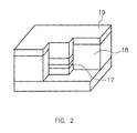
- FIG. 2 is a partly-cutaway perspective view illustrating an embodiment of a magnetoresistive element of the present invention.
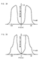
- FIGS. 3A and 3B are graphs showing MR characteristics of magnetoresistive elements according to an embodiment of the present invention.
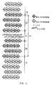
- FIG. 4 is a view illustrating a crystalline structure in the vicinity of a junction section of a magnetoresistive element according to an embodiment of the present invention.
- FIG. 5 is a view illustrating a crystalline structure in the vicinity of a junction section of a magnetoresistive element according to another embodiment of the present invention.
- FIG. 6A is a cross-sectional view of a magnetoresistive element according to an embodiment of the present invention
- FIG. 6B is a plan view of the foregoing element
- FIG. 6C is a cross-sectional view of a modification of the foregoing element.
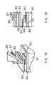
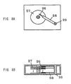
- FIG. 7A is a perspective view illustrating a schematic configuration of a magnetic head that is formed utilizing an element of the present invention
- FIG. 7B is a cross-sectional view of the foregoing head.
- FIG. 8A is a plan view illustrating an example of a magnetic disk device that is formed utilizing the magnetic heads shown in FIGS. 7A and 7B
- FIG. 8B is a cross-sectional view of the foregoing device.
- FIG. 9 is a cross-sectional view of a magnetic memory element that is formed utilizing magnetoresistive elements of the present invention.
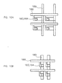
- FIGS. 10A and 10B are plan views each showing a wire layout in a magnetic memory element that is formed utilizing magnetoresistive elements of the present invention.
- FIG. 11A is a view illustrating a wire layout in a magnetic memory element of the present invention
- FIG. 11B is a view illustrating an example of a configuration of a magnetic memory device in which the magnetic memory elements are used.
- a ferromagnetic body obtains good contact with a layered perovskite structure oxide in the film thickness direction, and has an excellent conductivity.
- materials thereof desirably have good compatibility and are easily manufactured. Therefore, at least one of the ferromagnetic bodies desirably is made of a perovskite oxide, and more specifically, a complex oxide expressed by the formula: ((R 1-p L p ) 1-y A y ) m MO m+2-d where: A, R, M, and L represent the aforementioned elements, respectively; m represents 1 or 2; and d, p, and y represent numerical values satisfying 0 ⁇ d ⁇ 1, 0 ⁇ p ⁇ 1, and 0 ⁇ y ⁇ 1, respectively.
- This perovskite oxide ferromagnetic body exhibits improved compatibility with a layered-perovskite oxide at their junction interface when it is formed in contact with at least either an upper surface or a lower surface, or both, of the layered-perovskite oxide.
- the ferromagnetic body on the lower side (substrate side) preferably is selected so as to be made of a perovskite oxide.
- a combination of ferromagnetic bodes is a combination of a ferromagnetic body made of a perovskite oxide and a metallic ferromagnetic body. This pair is inferior in compatibility at the junction interface as compared with the case where both the ferromagnetic bodies are made of perovskite complex oxides, respectively.
- various excellent soft magnetic materials are available to form the metallic ferromagnetic body, and magnetic materials can be selected from a variety of soft and hard magnetic materials according to characteristics required of the element, thereby facilitating the control of the characteristics.
- a multilayer film formed on a substrate includes the aforementioned layered-perovskite oxide, and a pair of ferromagnetic bodies formed in contact with the layered-perovskite oxide so as to sandwich the layered-perovskite oxide, wherein, among the pair of the ferromagnetic bodies, the ferromagnetic body on the substrate side is made of a perovskite oxide, while the other ferromagnetic body (ferromagnetic body on a side opposite to the substrate) is made of a metallic ferromagnetic material.
- the pair of ferromagnetic bodies may be provided so that they have different coercive forces, and that they have different thicknesses. Further, an antiferromagnetic body may be provided so as to be in contact with either one of the ferromagnetic bodies.
- the antiferromagnetic body preferably is made of a perovskite oxide.
- a multilayer film formed on a substrate includes the aforementioned layered-perovskite oxide, and a pair of ferromagnetic bodies formed in contact with the layered-perovskite oxide so as to sandwich the layered-perovskite oxide, wherein one of the ferromagnetic bodies (preferably the ferromagnetic body on the substrate side) is made of a perovskite oxide, an antiferromagnetic body is provided in contact with the foregoing perovskite oxide ferromagnetic body, and further, an oxide electrode that will be described later is provided in contact with the antiferromagnetic body.
- p preferably is in the range of 0 ⁇ p ⁇ 0.3. From the same viewpoint, at least one of the ferromagnetic bodies and the layered-perovskite oxide more preferably contain the same element as the element L.
- the perovskite ferromagnetic oxide and the layered-perovskite oxide preferably satisfy 0.05 ⁇ y ⁇ 0.55 and 0.05 ⁇ 1-z ⁇ 0.55, respectively, in the aforementioned formulae.
- 0.8(1-z) ⁇ y ⁇ 1.2(1-z) preferably is satisfied.
- an oxide electrode preferably is provided in contact with a ferromagnetic body made of a perovskite oxide. More preferably the foregoing oxide electrode is made of a perovskite oxide.
- the oxide electrode preferably is a perovskite oxide having a higher electric conductivity than that of the ferromagnetic body made of a perovskite oxide.
- the oxide electrode made of a perovskite oxide preferably has a composition expressed by the following formula: (A 1-v R v ) j (X 1-r T r )O j+2-q where: A and R represent the aforementioned elements, respectively; T represents the same element as the element M contained in the ferromagnetic body in contact with the foregoing electrode (common element); X is at least one element (except the element T) selected from titanium (Ti), vanadium (V), copper (Cu), ruthenium (Ru), Nickel (Ni), and Chromium (Cr); j represents 1 or 2; and q, r, and v represent numerical values satisfying 0 ⁇ q ⁇ 1, 0 ⁇ r ⁇ 1, and 0 ⁇ v ⁇ 1, respectively.
- junction between the foregoing two can be maintained easily in a good state. From the same viewpoint, it is more preferable to satisfy 0.8y ⁇ 1-v ⁇ 1.2y.
- an element selected from the group consisting of Mn, Co, and Fe is suitable as the element M contained in the ferromagnetic body.
- an element contained as the elements T and M is preferably an element selected from the group essentially consisting of Ru, Ti, V, and Cu.
- a magnetoresistive element was formed in one vacuum chamber by sputtering, using Bi 2.4 (La 0.65 Sr 0.35 ) 2 Mn 1.2 O 6.9 , La 0.65 Sr 0.35 Mn 1.1 O 3.1 , and (La 0.65 Sr 0.35 )RuO 3 as target materials.
- the sputtering was conducted in a 0.5Pa argon atmosphere containing 20vol% of oxygen, with a discharge power of 50W, so as to form a film on a substrate heated to approximately 600°C.
- FIGS. 1A to 1C The process of forming the element is shown in FIGS. 1A to 1C: (La 0.65 Sr 0.35 )MnO 3 and (La 0.65 Sr 0.35 )RuO 3 were deposited in the stated order on a SrTiO 3 (100)-surface substrate 11 to thicknesses of 20nm and 50nm, respectively, to form a buffer layer 12 and a thin film 13 as a lower oxide electrode, respectively; then, a magnetoresistive tunnel junction layer 14 in which a Bi 2 (La 0.65 Sr 0.35 ) 2 MnO 6 thin film 21 was sandwiched between (La 0.65 Sr 0.35 )MnO 3 thin films 20 and 22 from above and below was formed thereon; further, (La 0.65 Sr 0.35 )RuO 3 was deposited thereon to a thickness of 20nm to form a thin film 15 as an upper oxide electrode (FIG.
- a thickness of the Bi 2 (La 0.65 Sr 0.35 )MnO 6 layer 21 was varied in a range of 0.4nm to 100nm in terms of a volume velocity. It was confirmed by X-ray diffraction and cross-section structure analysis that these thin films were grown with the c axis being oriented perpendicularly to the substrate surface. Subsequently, annealing was carried out in an oxygen-nitrogen mixture atmosphere at approximately 500°C to approximately 800°C.
- a photoresist 16 was formed, which was patterned so as to have an aspect ratio of 1:2.5, and an element width of 0.2 ⁇ m to 10 ⁇ m. It is preferable that the aspect ratio is 1.5/1 (1:1.5) or more since the anisotropy of magnetization of the ferromagnetic layer increases. In memory devices, the aspect ratio 5/1 (1:5) or less is appropriate for integration density.
- the element preferably has a round corner since it makes the rotation of the magnetization direction.
- FIG. 1B is a partly-cutaway perspective view of a portion of the junction thus formed.
- FIG. 3A illustrates a MR characteristic when (La 0.65 Sr 0.35 )MnO 3 , Bi 2 (La 0.65 Sr 0.35 ) 2 MnO 6 , and (La 0.65 Sr 0.35 )MnO 3 were 20nm, 1.5nm, and 15nm in thickness, respectively.
- Such a MR characteristic was obtained with good reproducibility when the Bi 2 (La 0.65 Sr 0.35 ) 2 MnO 6 in the junction layer had a thickness ranging from 1nm to 10nm.
- a preferable substitution rate of Ru to Mn was approximately 0.01% to 5%.
- (La,Sr)(Ru,Mn)O 3 , (La,Sr)MnO 3 , Bi 2 (La 0.65 Sr 0.35 ) 2 MnO 6 , (La,Sr)MnO 3 , and (La,Sr)(Ru,Mn)O 3 were deposited on (La,Sr)(Ru,Mn)O 3 .
- the alkaline earth element (A) and the rare earth element (R) were the same as the elements A and R of the ferromagnetic layers, respectively. These elements also were contained in the buffer layer.
- the barrier layer was present in crystal itself; that the manganese oxide and the barrier layer had good compatibility with each other; and that the magnetoresistive tunnel junction layer and the oxide electrode layers had good compatibility with each other. Since the foregoing element was particularly configured so that the magnetoresistive tunnel junction layer was provided on the substrate, with the buffer layer and the oxide electrode layer being interposed therebetween, a MR characteristic with further improved sensitivity was obtained as compared with an element without such layers.
- FIG. 4 schematically illustrates a crystalline structure in the vicinity of the junction interface of the oxide electrode layer to the magnetoresistive tunnel junction layer.
- FIG. 5 schematically illustrates, as another example, a crystalline structure in the vicinity of a junction interface in the case of a combination of a Bi 2 (La,Sr) 2 MnO 6 thin film (barrier layer: 21), (La,Sr) 2 MnO 4 thin films (ferromagnetic layers: 20, 22), and (La,Sr) 2 RuO 4 thin films (oxide electrodes: 13, 15).
- crystalline structures of the magnetoresistive tunnel junction layer and the oxide electrode layer in the vicinity of the interface therebetween have good compatibility, and so do those of the ferromagnetic layer and the barrier layer in the vicinity of the interface therebetween. It is considered that with such excellent junction, it was possible to provide a magnetoresistive tunnel junction element with high sensitivity.
- a MR characteristic was obtained at a further lower magnetic field as compared with the characteristic results of the (La 0.67 Sr 0.33 )MnO 3 / SrTiO 3 (6nm) / (La 0.67 Sr 0.33 )MnO 3 junction proposed by Y. Lu et al. (Y. Lu et al. : Phys. Rev. Lett. 54(1996)R8357 supra ). This seems to have resulted from smooth continuity of structures as shown in FIGS. 4 and 5 that in turn realized a junction interface having good continuity.
- substitution of a part of Sr (A) with a rare earth element (0 ⁇ y ⁇ 1) is preferable, from the viewpoint of the stability of the element structure.
- an oxide electrode layer may be provided directly on the substrate, considering compatibility with a junction layer including ferromagnetic layers.
- a magnetoresistive element was formed in one vacuum chamber by sputtering, using (La 0.65 Sr 0.35 )Mn 1.2 O 3.1 , Bi 2.4 (La 0.65 Sr 0.35 ) 2 CaCu 2.4 O 8 , and (La 0.85 Sr 0.15 ) 2 CuO 4 as target materials.
- the sputtering was conducted in a 0.5Pa argon atmosphere containing 20vol% of oxygen with discharge power of 50W, so as to form a film on a substrate heated to approximately 600°C.
- (La 0.85 Sr 0.15 ) 2 CuO 4 was deposited to a thickness of 50nm on a SrTiO 3 (100)-surface substrate. Thereon, a 50nm-thick (La 0.65 Sr 0.35 )MnO 3 thin film, a Bi 2 (La 0.65 Sr 0.35 ) 2 CaCu 2 O 8 thin film, a 50nm-thick La 0.65 Sr 0.35 MnO 3 thin film, and a 20nm-thick (La 0.85 Sr 0.15 ) 2 CuO 4 thin film were formed in the stated order.
- the thickness of the Bi 2 (La 0.65 Sr 0.35 ) 2 CaCu 2 O 8 thin film was varied in a range of 0.4nm to 50nm in terms of volume velocity. It was confirmed that these thin films were grown with the c axis being oriented perpendicularly to the substrate surface.
- a photoresist was formed, which was patterned so as to have an aspect ratio of 1:2.5, and an element width of 0.2 ⁇ m to 10 ⁇ m. Thereafter, etching was carried out with argon ions, so that a junction section was carved out. Thereafter, an Al 2 O 3 thin film was formed as an interlayer insulating-separating layer, and then a lead electrode was formed by using Cu and Pt. Thus, the element was finished.
- the junction thus formed was in an identical shape to that shown in FIGS. 1 and 2.
- FIG. 3B illustrates a MR characteristic when the Bi 2 (La 0.65 Sr 0.35 ) 2 CaCu 2 O 8 film was 3nm thick. Such a MR characteristic was obtained with good reproducibility when the Bi 2 (La 0.65 Sr 0.35 ) 2 CaCu 2 O 8 thin film had a thickness ranging from 1.5nm to 10nm.
- Bi 2 (La 0.65 Sr 0.35 ) 2 CaCu 2 O 8 is a substance that as a bulk exhibits superconductivity at not higher than approximately 70K. Additionally, also the oxide electrode (La 0.85 Sr 0.15 ) 2 CuO 4 , which also functions as a buffer layer, as a bulk exhibits superconductivity at not higher than approximately 30K. Therefore, no electrode resistance appeared in the TMR characteristic evaluated at not higher than 4.2K in a four-electrode configuration, and hence a characteristic of the junction per se could be evaluated. To obtain superconductivity, the oxide electrode is preferably made of a material expressed as (La 1-x Sr x ) 2 CuO 4 where x satisfies 0.05 ⁇ x ⁇ 0.3. Further, to obtain superconductivity with the layered-perovskite complex oxide, the oxide preferably is expressed as Bi 2 (Sr,Ca) 3-x La x Cu 2 O 8 where x satisfies 0 ⁇ x ⁇ 0.5.
- a magnetoresistive element was formed in one vacuum chamber by laser ablation, using (La 0.85 Sr 0.15 ) 2 Cu 1.2 O 4.2 , Tl 2 Ba 2 Ca 2 Mn 3 O 12 , and Tl 2 Mn 2 O 7 as target materials.
- the target ablation was conducted in an oxygen atmosphere at 5Pa to 70Pa with laser power of approximately 1 to 5 J/cm 2 , so as to form a film on a substrate heated to approximately 600°C to 700°C.
- LaCuO 3 and (La 0.85 Sr 0.15 ) 2 CuO 4 were deposited, on a SrTiO 3 (100)-surface substrate to thicknesses of 20nm and 50nm, respectively, to form a buffer layer and a thin film as a lower oxide electrode, respectively.
- a junction layer composed of a (La 0.8 Sr 0.2 )MnO 3 thin film, a Tl 2 Ba 2 Ca 2 Mn 3 O 12 thin film, and a Tl 2 Mn 2 O 7 thin film were formed, on which (La 0.85 Sr 0.15 ) 2 CuO 4 was deposited to a thickness of 20nm to form a thin film as an upper oxide electrode.
- the junction layer was configured so that the thin films of (La 0.8 Sr 0.2 )MnO 3 , Tl 2 Ba 2 Ca 2 Mn 3 O 12 , and Tl 2 Mn 2 O 7 were 20nm, 4.5nm, and 25nm in thickness, respectively. It was confirmed that these thin films were grown with the c axis being oriented perpendicularly to the substrate surface.
- Tl 2 Mn 2 O 7 is a pyrochlore-type oxide.
- a photoresist was formed, which was patterned so as to have an aspect ratio of 1:2.5 and an element width of 0.2 ⁇ m to 10 ⁇ m. Thereafter, etching was carried out with argon ions, so that a junction section was carved out. Thereafter, a CaF 2 thin film was formed as an insulating-separating layer, and then a lead electrode was formed with gold. Thus, the element was finished.
- the junction thus formed was in an identical shape to that shown in FIGS. 1 and 2.
- MR magnetoresistive
- the same MR characteristic was recognized when another rare earth element (R) was used, and excellent reproducibility was obtained particularly when any one of La, Pr, Nd, and Sm was used.
- a 50nm-thick SrRuO 3 thin film and a 50nm-thick LaFeO 3 thin film were formed in the stated order on a SrTiO 3 (100)-surface substrate by sputtering as described above. Thereon, a junction layer composed of a 5nm-thick (La 0.6 Bi 0.05 Sr 0.35 )MnO 3 thin film, a 3nm-thick Bi 2 (La 0.65 Sr 0.35 ) 2 MnO 6 thin film, and a 10nm-thick (La 0.6 Bi 0.05 Sr 0.35 )MnO 3 film were formed.
- the sputtering was conducted also under the conditions of a 0.5Pa argon atmosphere containing 20% of oxygen and discharge power of 50W, but the substrate temperature was set to approximately 650°C.
- the thickness of the Bi 2 (La 0.65 Sr 0.35 ) 2 MnO 6 thin film was varied in a range of 0.4nm to 10nm in terms of a volume velocity. It was confirmed that these thin films were grown with the c axis being oriented perpendicularly to the substrate surface. Subsequently, annealing was carried out in an oxygen-nitrogen mixture atmosphere at approximately 500°C to approximately 800°C.
- the substrate was cooled to room temperature, and Ni-Co-Fe, Ni 0.8 Fe 0.2 , and Ta were deposited to form thin films of approximately 50nm, 10nm, and 10nm in thickness, respectively.
- a photoresist was formed, which was patterned in an element area of 0.35 ⁇ m ⁇ 7 ⁇ m, and thereafter, etching was carried out with argon ion, so that a junction section was carved out. Thereafter, a SiO 2 thin film was formed as an insulating-separating layer, and then a lead electrode was formed. Thus, the element was finished.
- the SrRuO 3 thin film was a lower oxide electrode that also functions as a buffer layer
- the LaFeO 3 thin film was an antiferromagnetic body, which caused the (La 0.6 Bi 0.05 Sr 0.35 )MnO 3 thin film in contact therewith to be a pinned ferromagnetic layer.
- the LaFeO 3 thin film was a perovskite oxide as well.
- the Ta thin film was a base film on which a wire electrode material (herein, mainly Cu) was to be provided.
- MR magnetoresistive
- LaFeO 3 as a bulk exhibits antiferromagnetism at the measurement temperature.
- SrTiO 3 (100) which is a cubic substance, was used to form the substrate, but a cubic substance such as LaSrGaO 4 (001), an orthorhombic substance such as LaAlO 3 (001), YAlO 3 (001), Nd:YAlO 3 (001), or LaGaO 3 (001), or another cubic substance (for instance, MgO) may be used. Further, Nd:SrTiO 3 (100), for instance, may be used so that an electrode body can be used as the substrate.
- an in-plane-type magnetoresistive element was formed utilizing an oblique substrate as shown in FIG. 6.
- a SrTiO 3 (001)-surface substrate having a tilt of approximately 1° in the [100] direction was used as a substrate 43.
- the surface of the substrate included terrace surfaces.
- a 1nm to 20nm-thick (La 0.65 Sr 0.35 )MnO 3 thin film, a 1.5nm to 10nm-thick Bi 2 (La 0.6 Sr 0.4 )CaMnO 6 thin film, a 1nm to 20nm-thick (La 0.65 Sr 0.35 )MnO 3 thin film, and a 5nm to 100nm-thick SrRuO 3 thin film were formed in the stated order on the substrate, so as to form a laminated body 41 including a junction layer.
- the film formation was carried out by sputtering, in an 0.5Pa argon atmosphere containing 20% of oxygen, with discharge power of 50W, onto a substrate heated to approximately 650°C.
- FIGS. 6A and 6B An element structure as shown in FIGS. 6A and 6B was obtained by submicron processing by exposure utilizing a stepper or an electron beam.
- a laminated body 41 was formed on an oblique substrate surface 47 of the foregoing substrate by growing while forming steps. This is because crystal growth of the base materials was reflected. On portions 44 unconformable with the steps, hetero-phase substances were provided.
- FIG. 6A shows steps of the laminated body 41 that are provided at a cycle three times a cycle of the steps of the substrate, but the configuration is not limited to this. There are many patterns, and it was confirmed that elements are formed where steps are provided at a cycle of three to ten times.
- an Al 2 O 3 thin film was formed as a cover layer 45, so as to cover the element.
- An area processed to be an element was approximately 50nm (W) ⁇ approximately 100nm (L) (FIG. 6B). It was confirmed that a MR effect was obtained from the element thus formed, at a low magnetic field of several tens G.
- the substrate material also is not particularly limited to the SrTiO 3 (001)-surface substrate.
- Table 1 Materials of the foregoing element that were confirmed to provide a MR effect are shown in Table 1.
- the film A is equivalent to the SrRuO 3 film in the foregoing example, while the film B is equivalent to the La 0.65 Sr 0.35 MnO 3 thin film in the foregoing example.
- the other thin films were configured as described above.
- the size of the junction section is that shown in FIG. 6B (L ⁇ W).
- FILM A FILM B MR VALUE JUNCTION SECTION (nm) Bi 2 (La 0.65 Sr 0.35 ) 2 CuO 6 (La 0.65 Sr 0.35 ) 2 MnO 4 68% (20K) 50 ⁇ 30 Bi 2 (La 0.65 Sr 0.35 ) 2 RuO 6 (La 0.65 Sr 0.35 ) 2 MnO 4 34% (room temp.) 80 ⁇ 40 Bi 2 (La 0.65 Sr 0.35 ) 2 RuO 6 NiMnSb 28% (room temp.) 70 ⁇ 40
- a processed substrate in a stepped shape as shown in FIG. 6C may be used. It was confirmed that an element using the stepped substrate through the process described above (the junction section was 50nm ⁇ 50nm in size) provided an identical MR effect. It was recognized that the resistance of the element tended to increase when the stepped substrate was used, as compared with the case where the oblique substrate was used.
- the two types of substrates may be selected according to the element characteristics needed.
- the step angle is not limited to the right angle and is preferably about 70° to about 90°.
- a magnetic head was produced using a magnetoresistive element.
- FIGS. 7A and 7B A configuration of the magnetoresistive head produced is shown in FIGS. 7A and 7B. Incidentally, sputtering was carried out for film formation.
- single crystal SrTiO 3 was used to form a substrate 81
- a (La 0.65 Sr 0.35 )RuO 3 thin film was used to form a lower shield layer 82
- NiFe alloy thin films were used to form an upper shield layer 83 and recording magnetic poles 85 and 86 disposed above and below a coil 87.
- Each of the shield layers was 100nm thick, while each of the recording magnetic poles was 3 ⁇ m thick.
- Each gap layer between the foregoing layers was formed with a SrTiO 3 thin film.
- Each of the gap layers between the shield layers and the magnetoresistive element 84 had a thickness of 0.1 ⁇ m, and each of those between the shield layers and the recording magnetic poles had a thickness of 0.2 ⁇ m.
- a gap between a reproducing head and a recording head was set to approximately 4 ⁇ m, and a gap layer for the gap was formed with an Al 2 O 3 thin film.
- An insulator section 95 separates the magnetoresistive element 84 from a head surface 88, so as not to be exposed directly on the head surface 88.
- a lead electrode 89 was formed mainly with Cu, and a lead electrode 91 was formed with (La 0.65 Sr 0.35 )RuO 3 .
- a coil was formed with a 3 ⁇ m-thick Cu thin film. SrTiO 3 was used to form the insulator section 95.
- the magnetoresistive element 84 was configured by laminating the following thin films in the stated order: a (La 0.65 Sr 0.35 ) 2 MnO 4 thin film or a (La 0.65 Sr 0.35 )MnO 3 thin film, 20nm thick, as a lower ferromagnetic layer; a Bi 2 (La 0.65 Sr 0.35 ) 2 MnO 6 thin film, 3nm thick, as a junction layer; and a Ni-Fe-Co- thin film, 50nm thick, as an upper ferromagnetic layer.
- a composition of the Ni-Fe-Co is preferably Ni-rich, or Co-rich, as described above.
- a 50nm-thick thin film either made of Ni 81 Fe 19 or having the same composition as that of the upper ferromagnetic layer was used to form a magnetic layer 90 that was in contact with the upper ferromagnetic layer.
- the two ferromagnetic layers in the foregoing magnetoresistive element 84 were formed so that magnetization directions crossed each other at right angles.
- a bias current across the electrodes 89 and 91 Upon application of a bias current across the electrodes 89 and 91, a shift of the magnetization direction of the upper ferromagnetic layer according to a magnetic field applied thereto via the magnetic layer 90 was read as a change in the magnetic resistance, based on which a signal was reproduced.
- FIGS. 8A and 8B illustrate an example of a magnetic disk device using a magnetic head.
- the magnetic head 96 was attached at an end of a magnetic head supporting section 98, and was driven by a magnetic head driving section 99 provided at the other end of the supporting section 98.
- a plurality of the magnetic heads 96 and magnetic disks were used in a state of being stratified in a disk thickness direction.
- a width of a track may be, for instance, set to 5 ⁇ m.
- the magnetoresistive element 84 exhibited a higher resistance change, and hence a higher reproducing power, than a conventional GMR element of the CIPMR type did; therefore the magnetoresistive element 84 excelled as a reproduction-use magnetic head.
- a magnetic disk device produced using the element 84 thus formed was capable of detecting voltage changes according to signals recorded in a magnetic recording medium with good sensitivity.
- the magnetic head discussed in the present embodiment is configured so that magnetoresistive tunnel current flows upon application of a current bias, by providing a pair of ferromagnetic bodies sandwiching the foregoing layered-perovskite oxide therebetween, one of the ferromagnetic layers being a free ferromagnetic layer, the other being a pinned ferromagnetic layer in contact with an antiferromagnetic layer.
- the pinned ferromagnetic layer and the free ferromagnetic layer are magnetized beforehand in directions crossing each other at right angles.
- a MRAM device as a magnetic recording element was produced by providing magnetoresistive elements as recording cells in a matrix form. Herein also the sputtering method was applied.
- Techniques for recording and reading information to and from a magnetic memory element include a technique utilizing a difference between coercive forces and a technique utilizing a combination of a free layer and a pinned layer.
- memory information is read out in the following manner: magnetization directions are recorded in a layer having a relatively greater coercive force, and a magnetization of a layer having a relatively smaller coercive force is inverted by applying an external magnetic field having a smaller force than that of the magnetic field applied previously; a change occurs in the resistance of the element according to parallel and antiparallel alignments of magnetization in the two layers, and memory information is read out according to the change.
- one of ferromagnetic layers is provided adjacent to an antiferromagnetic body so that magnetization directions thereof are pinned, while the other ferromagnetic layer is used as a free layer whose magnetization is easily inverted by an external magnetic field, so that memory information is recorded and read out according to changes in the resistance of the element according to parallel and antiparallel alignments of magnetizations in the pinned layer and the free layer.
- the magnetoresistive element according the present invention can be applied to a memory element using a pinned layer and a free layer, but herein a demonstration was carried out using a configuration utilizing the coercive force difference.
- (La 0.65 Sr 0.35 )RuO 3 was deposited to a thickness of 50nm on a substrate 181 formed with single crystal SrTiO 3 , to form a thin film serving as a buffer layer and a lower oxide electrode 182.
- the buffer layer-lower oxide electrode 182 there was provided either a multilayer film formed with (La 0.85 Sr 0.15 )MnO 3 (50nm), SrTiO 3 (100nm), and (La 0.95 Sr 0.05 )TiO 3 (50nm), or a multilayer film formed with (Li 0.01 Ni 0.99 )O (50nm), SrTiO 3 (100nm), and (La 0.95 Sr 0.05 )TiO 3 (50nm). Both of the multilayer films 183 had remarkable asymmetry as to electric properties, and exhibited characteristics like a diode.
- a magnetoresistive element 184 a La 1.4 Ca 1.6 Mn 2 O 7 thin film (20nm) as a lower ferromagnetic layer, a (Bi 0.95 Pb 0.05 ) 2 (Sr 0.75 Ca 0.25 )CaMn 2 O 9 thin film (2nm), and a (La 0.7 Ca 0.3 )MnO 3 thin film (20nm) as an upper ferromagnetic layer were laminated thereon in the stated order. Further, (La 0.65 Sr 0.35 )RuO 3 was deposited thereon to a thickness of 20nm so as to form a thin film serving as an oxide electrode, and a lead electrode 185 was formed using Au.
- La 1.4 Ca 1.6 Mn 2 O 7 is expressed as (La,Ca) 3 Mn 2 O 7 , and is an analogous compound having a structure in which (La,Ca)MnO 3 and (La,Ca) 2 MnO 4 are cyclically laminated.
- Al 2 O 3 , CaF 2 , and SiO 2 were used to form interlayer insulating films 186.
- the lead electrode 185 was connected to an electrode that constitutes a bit line 188, and the buffer layer 182 was connected to an electrode that constitutes a sensing line 189.
- Current-voltage characteristics were examined as to a single piece of a magnetoresistive element of the coercive force difference type thus formed, and it was confirmed that the element exhibited remarkable asymmetry and excellent magnetoresistance effect characteristics.
- Magnetoresistive elements formed as above were arrayed in a matrix form as shown in FIG. 10A, with interlayer insulating films being provided to isolate each of the elements, and upper electrodes were provided in a direction crossing lower electrodes at right angles.
- the upper and lower electrodes were used as bit lines 188 and sense lines 189 of the MRAM, respectively.
- the magnetoresistive elements 184 may be formed on the lower electrodes (sense line 189), so that the sense lines also can be used as wires for generation of a magnetic field.
- word lines 187 were provided so as to cross the sense lines at right angles.
- a basic structure of the MRAM was formed.
- AuCr or Cu was used to form conductive films used as sense lines
- Au or Cu was used to form conductive films used as word lines
- Al 2 O 3 was used for insulation between the memory elements and the word lines.
- a 256 ⁇ 256 matrix-form memory was configured.
- the matrix-form memory was provided with sense lines 111, bit lines 112, and word lines 113 and 114 as illustrated in FIG. 11A.
- Magnetoresistive elements 116 each constituting a memory cell, were provided between the sense lines and the bit lines.
- word lines were used for each, in order to improve writing selectivity.
- Nodes of the lines are illustrated with dots 115, respectively, for convenience.
- the MRAM device was provided with switching sections (118 for the sense lines, 119 for the bit lines, 117 and 120 for word lines) for addressing, signal path transistor sections 123 that, in response to the addressing, determine availability of the address for writing or reading by turning on/off, a signal resistance detecting section 121, and a word-line-use signal detecting section 122, with which information recording and reproduction was carried out.
- the storing was carried out as follows: current pulses are sent through the word lines as row elements and column elements, and a magnetic field thereby generated causes a magnetization of a specific element to change.
- a memory element at a specific address is selected by a first addressing switch section, and a current pulse selected by a second addressing switch section that generates a magnetic field to affect only the foregoing selected memory element at the specific address so as to invert the magnetization direction of the ferromagnetic film thereof having the smaller coercive force is applied to the foregoing selected memory element through either the word line as the row element or the word line as the column element, while a resistance of the selected memory element is monitored using the sense line.
- the magnetic recording element discussed in the description of the present embodiment is provided with a pair of ferromagnetic bodies sandwiching a layered-perovskite oxide that exhibits a magnetoresistive tunnel effect upon the application of a bias, and at least one non-magnetic conductive layer for generating an external magnetic field, electrically out of contact with the foregoing ferromagnetic bodies, wherein one of the ferromagnetic bodies is a free ferromagnetic layer, while the other is a pinned ferromagnetic layer.
- the foregoing magnetic recording element operates through:
- Film formation was carried out by sputtering so that a multilayer film as described below was formed in one vacuum chamber.
- the multilayer film was formed onto a substrate heated to approximately 600°C to 800°C.
- SrVO 3 was deposited to 50nm in thickness on a SrTiO 3 (100)-surface substrate, to form a layer to function both as a buffer layer and an oxide electrode layer.
- (Sr,Ca) 2 FeMO 6 used herein is a material composed of two kinds of perovskite materials having a perovskite structure of AB(1)O 3 -AB(2)O 3 that is called double perovskite.
- A Sr,Ca
- B(1) Fe
- B(2) Mo,Re.
- La 1.4 Sr 1.6 Mn 2 O 7 is a material composed of two perovskite analogous compounds expressed as (La,Sr) 2 MnO 4 -(La,Sr)MnO 3 .
- a photoresist was formed, which was patterned so as to have an aspect ratio of 1:2.5, and an element width of 0.2 ⁇ m to 10 ⁇ m.
- etching was carried out with argon ions, so that a junction section was carved out. Thereafter, an insulating-separating layer was formed with a CaF 2 thin film, and a lead electrode made of gold was provided, whereby the element was finished.
- the outcome of measurement at approximately 20K proved that a MR characteristic was observed with any composition.
- x in (Sr 1-x Ca x ) 2 FeMO 6 preferably is less than 1, since Ca 2 FeMO 6 has an electric conductivity in closer approximation to that of a semiconductor thereby having an excessively great resistance as a ferromagnetic electrode.
- a multilayer film as described below was formed in one vacuum chamber.
- the multilayer film was formed onto a substrate heated to approximately 600°C to 800°C.
- SrVO 3 was deposited to 50nm in thickness on a SrTiO 3 (100)-surface substrate, to form a layer to function both as a buffer layer and an oxide electrode layer.
- a photoresist was formed, which was patterned so as to have an aspect ratio of 1:2.5, and an element width of 0.2 ⁇ m to 10 ⁇ m. Then, etching was carried out with argon ions, so that a junction section was carved out. Thereafter, an insulating-separating layer was formed with a CaF 2 thin film, and a lead electrode made of gold was provided, whereby the element was finished. The outcome of measurement at room temperature proved that a MR characteristic was observed with any composition, therefore it was confirmed that the magnetoresistive element of the present invention was effective.
- the present invention used is an insulating layer involved in a layer perovskite oxide that is capable of functioning not only at a low temperature but also at room temperature in response to a low magnetic field, hence, it is possible to provide an element having a magnetoresistive tunnel junction characteristic with high sensitivity.
- the present invention is to provide basic element components of magnetic devices, and to make a great contribution in the development of magnetic devices.
Landscapes
- Engineering & Computer Science (AREA)
- Chemical & Material Sciences (AREA)
- Nanotechnology (AREA)
- Physics & Mathematics (AREA)
- Mathematical Physics (AREA)
- Theoretical Computer Science (AREA)
- Crystallography & Structural Chemistry (AREA)
- Manufacturing & Machinery (AREA)
- Hall/Mr Elements (AREA)
- Thin Magnetic Films (AREA)
- Compounds Of Iron (AREA)
Abstract
Description
| FILM A | FILM B | MR VALUE | JUNCTION SECTION (nm) |
| Bi2(La0.65Sr0.35)2CuO6 | (La0.65Sr0.35)2MnO4 | 68% (20K) | 50×30 |
| Bi2(La0.65Sr0.35)2RuO6 | (La0.65Sr0.35)2MnO4 | 34% (room temp.) | 80×40 |
| Bi2(La0.65Sr0.35)2RuO6 | NiMnSb | 28% (room temp.) | 70×40 |
Claims (20)
- A magnetoresistive element comprising:where:a layered-perovskite oxide having a composition expressed by a formula L2(A1-zRz)2An-1MnO3n+3+x and including a (L-O)2 layer in its crystalline structure;a pair of ferromagnetic bodies formed in contact with the layered-perovskite oxide so as to sandwich the oxide.A represents at least one alkaline earth element selected from the group consisting of Ca, Sr, and Ba;L represents at least one element selected from the group consisting of Bi, Tl, and Pb;M represents at least one element selected from the group consisting of Ti, V, Cu, Ru, Ni, Mn, Co, Fe, and Cr;R represents a rare earth element;n is 1, 2, or 3; andx and z are numerical values satisfying -1≤x≤1, and 0≤z<1, respectively.
- The magnetoresistive element as claimed in claim 1, the element further comprising an oxide electrode, wherein at least one of the pair of ferromagnetic bodies is made of a perovskite oxide, and the oxide electrode is provided in contact with the ferromagnetic body made of a perovskite oxide.
- The magnetoresistive element as claimed in claim 2, wherein the ferromagnetic body made of a perovskite oxide has a composition expressed by a formula ((R1-pLp)1-yAy)mMOm+2-d,
where:A, L, M, and R represent the same elements as those set forth in claim 1, respectively;m is 1 or 2; andd, p, and y are numerical values satisfying 0≤d≤1, 0≤p≤1, and 0≤y≤1, respectively. - The magnetoresistive element as claimed in claim 3, wherein p is a numerical value satisfying 0<p≤1.
- The magnetoresistive element as claimed in claim 4, wherein the ferromagnetic body made of a perovskite oxide and the layered-perovskite oxide layer contain the same element for the element L.
- The magnetoresistive element as claimed in any one of claims 3 to 5, wherein y and z satisfy 0.05≤y≤0.55 and 0.05≤1-z≤0.55, respectively.
- The magnetoresistive element as claimed in any one of claims 3 to 6, wherein relationship 0.8(1-z)≤y≤1.2(1-z) is satisfied.
- The magnetoresistive element as claimed in any one of claims 2 to 7, wherein the oxide electrode is made of a perovskite oxide.
- The magnetoresistive element as claimed in claim 8, wherein the oxide electrode made of a perovskite oxide has a composition expressed by a formula (A1-vRv)j(X1-rTr)Oj+2-q,
where:A and R represent the same elements as those set forth in claim 1, respectively;T represents the same element as the element M contained in the ferromagnetic body in contact with the oxide electrode;X represents at least one element selected from the group consisting of Ti, V, Cu, Ru, Ni, and Cr (except the element T);j is 1 or 2; andq, r, and v are numerical values satisfying 0≤q≤1, 0≤r≤1, and 0≤v≤1, respectively. - The magnetoresistive element as claimed in claim 9, wherein r satisfies 0<r≤1.
- The magnetoresistive element as claimed any one of claims 1 to 10, wherein one of the pair of ferromagnetic bodies is made of a perovskite oxide, and the other is made of a metallic ferromagnetic material.
- The magnetoresistive element as claimed in claim 11, wherein the metallic ferromagnetic material contains a ferromagnetic material expressed by a formula NixCoyFez, where x, y, and z are numerical values satisfying x+y+z=1 and one of the following (i) and (ii):(i) 0.6≤x≤0.9, 0≤y≤0.4, and 0≤z≤0.3(ii) 0≤x≤0.4, 0.2≤y≤0.95, and 0≤z≤0.5
- The magnetoresistive element as claimed in claim 11, wherein the metallic ferromagnetic material contains a ZMnSb alloy ferromagnetic material, where Z represents at least one element selected from the group consisting of Ni, Pt, and Pd.
- The magnetoresistive element as claimed in any one of claims 1 to 13, wherein the ferromagnetic bodies in the pair have different coercive forces.
- The magnetoresistive element as claimed in any one of claims 1 to 14, wherein the ferromagnetic bodies in the pair have different thicknesses.
- The magnetoresistive element as claimed in any one of claims 1 to 15, wherein the rare earth element R is at least one selected from the group consisting of La, Pr, Nd, and Sm.
- The magnetoresistive element as claimed in claim 16, wherein both the antiferromagnetic body and the ferromagnetic body in contact with the antiferromagnetic body are made of a perovskite oxide, respectively.
- The magnetoresistive element as claimed in any one of claims 1 to 17, wherein the rare earth element R is at least one selected from the group consisting of La, Pr, Nd, and Sm.
- A magnetic memory element comprising the magnetoresistive element as claimed in any one of claims 1 to 18.
- A magnetic head comprising the magnetoresistive element as claimed in any one of claims 1 to 18.
Applications Claiming Priority (2)
| Application Number | Priority Date | Filing Date | Title |
|---|---|---|---|
| JP2000152380 | 2000-05-24 | ||
| JP2000152380 | 2000-05-24 |
Publications (2)
| Publication Number | Publication Date |
|---|---|
| EP1162672A2 true EP1162672A2 (en) | 2001-12-12 |
| EP1162672A3 EP1162672A3 (en) | 2003-11-26 |
Family
ID=18657810
Family Applications (1)
| Application Number | Title | Priority Date | Filing Date |
|---|---|---|---|
| EP01304546A Withdrawn EP1162672A3 (en) | 2000-05-24 | 2001-05-23 | Magnetoresistive element and magnetic memory element and magnetic head using the same |
Country Status (4)
| Country | Link |
|---|---|
| US (1) | US6594120B2 (en) |
| EP (1) | EP1162672A3 (en) |
| KR (1) | KR100451871B1 (en) |
| CN (1) | CN1190856C (en) |
Cited By (2)
| Publication number | Priority date | Publication date | Assignee | Title |
|---|---|---|---|---|
| EP1455363A1 (en) * | 2003-03-06 | 2004-09-08 | Sharp Kabushiki Kaisha | Non-volatile semiconductor memory device |
| CN110808331A (en) * | 2019-11-19 | 2020-02-18 | 郑州工程技术学院 | Giant magnetoresistance film and preparation method thereof |
Families Citing this family (17)
| Publication number | Priority date | Publication date | Assignee | Title |
|---|---|---|---|---|
| US7205056B2 (en) * | 2001-06-13 | 2007-04-17 | Seiko Epson Corporation | Ceramic film and method of manufacturing the same, ferroelectric capacitor, semiconductor device, and other element |
| US7211199B2 (en) * | 2002-03-15 | 2007-05-01 | The Trustees Of The University Of Pennsylvania | Magnetically-and electrically-induced variable resistance materials and method for preparing same |
| US7309903B2 (en) * | 2002-03-26 | 2007-12-18 | Japan Science And Technology Agency | Tunneling magnetoresistance device semiconductor junction device magnetic memory and semiconductor light-emitting device |
| CN100369117C (en) * | 2002-12-31 | 2008-02-13 | 有研稀土新材料股份有限公司 | Oxide giant magnet resistor spin valve, preparing process and its use |
| JP4120589B2 (en) * | 2004-01-13 | 2008-07-16 | セイコーエプソン株式会社 | Magnetoresistive element and magnetic memory device |
| US7183893B2 (en) * | 2004-02-04 | 2007-02-27 | Seagate Technology Llc | TMR sensor with oxidized alloy barrier layer and method for forming the same |
| ATE446581T1 (en) * | 2004-03-12 | 2009-11-15 | Trinity College Dublin | MAGNETORRESISTIVE MEDIUM |
| US8107194B2 (en) | 2008-09-24 | 2012-01-31 | International Business Machines Corporation | Writing and reading multi-layer continuous magnetic recording media |
| US7911739B2 (en) * | 2008-09-25 | 2011-03-22 | International Business Machines Corporation | Writing and reading multi-level patterned magnetic recording media |
| US8304754B2 (en) * | 2008-11-12 | 2012-11-06 | Sandisk 3D Llc | Metal oxide materials and electrodes for Re-RAM |
| FR2939955B1 (en) * | 2008-12-11 | 2011-03-11 | Commissariat Energie Atomique | METHOD FOR PRODUCING MAGNETIC TUNNEL JUNCTION AND MAGNETIC TUNNEL JUNCTION THUS OBTAINED |
| US8031425B2 (en) * | 2009-11-10 | 2011-10-04 | International Business Machines Corporation | Writing and reading multi-layer continuous magnetic recording media, with more than two recording layers |
| US8085502B2 (en) * | 2009-11-10 | 2011-12-27 | International Business Machines Corporation | Writing and reading multi-level patterned magnetic recording media, with more than two recording levels |
| TWI482155B (en) * | 2010-07-05 | 2015-04-21 | Macronix Int Co Ltd | Nonvolatile memory device having trasistor connected in parallel with resistance switching device |
| WO2012140971A1 (en) | 2011-04-14 | 2012-10-18 | 富士電機株式会社 | Perovskite-type manganese oxide thin film |
| JP2019054054A (en) * | 2017-09-13 | 2019-04-04 | 東芝メモリ株式会社 | Magnetic device |
| US10559412B2 (en) * | 2017-12-07 | 2020-02-11 | Tdk Corporation | Magnetoresistance effect device |
Family Cites Families (9)
| Publication number | Priority date | Publication date | Assignee | Title |
|---|---|---|---|---|
| JP2956299B2 (en) * | 1991-08-30 | 1999-10-04 | 株式会社日立製作所 | Magnetic detecting element, energy detecting element, and energy detecting method |
| DE4425356C2 (en) * | 1993-09-29 | 1998-07-02 | Siemens Ag | Magnetoresistive sensor using a sensor material with a perovskite-like crystal structure |
| JP2734422B2 (en) * | 1995-07-20 | 1998-03-30 | 日本電気株式会社 | Compound magnetoresistive material and method for producing the same |
| JP3593761B2 (en) * | 1995-10-26 | 2004-11-24 | 富士通株式会社 | Oxide magnetic body and method of manufacturing the same |
| US5792569A (en) * | 1996-03-19 | 1998-08-11 | International Business Machines Corporation | Magnetic devices and sensors based on perovskite manganese oxide materials |
| JP3325478B2 (en) * | 1996-12-27 | 2002-09-17 | ワイケイケイ株式会社 | Magnetoresistive element, magnetic detector and method of using the same |
| JPH1186236A (en) * | 1997-09-05 | 1999-03-30 | Toshiba Corp | Magnetic element, magnetic memory and magneto-optical element |
| JP2000012920A (en) | 1998-06-24 | 2000-01-14 | Matsushita Electric Ind Co Ltd | Magnetoresistive tunnel junction device |
| JP2000012921A (en) | 1998-06-24 | 2000-01-14 | Matsushita Electric Ind Co Ltd | Magnetoresistive tunnel junction device |
-
2001
- 2001-05-23 US US09/864,564 patent/US6594120B2/en not_active Expired - Lifetime
- 2001-05-23 EP EP01304546A patent/EP1162672A3/en not_active Withdrawn
- 2001-05-23 KR KR10-2001-0028377A patent/KR100451871B1/en not_active Expired - Fee Related
- 2001-05-24 CN CNB011220627A patent/CN1190856C/en not_active Expired - Fee Related
Cited By (3)
| Publication number | Priority date | Publication date | Assignee | Title |
|---|---|---|---|---|
| EP1455363A1 (en) * | 2003-03-06 | 2004-09-08 | Sharp Kabushiki Kaisha | Non-volatile semiconductor memory device |
| US7002837B2 (en) | 2003-03-06 | 2006-02-21 | Sharp Kabushiki Kaisha | Non-volatile semiconductor memory device |
| CN110808331A (en) * | 2019-11-19 | 2020-02-18 | 郑州工程技术学院 | Giant magnetoresistance film and preparation method thereof |
Also Published As
| Publication number | Publication date |
|---|---|
| KR100451871B1 (en) | 2004-10-08 |
| CN1190856C (en) | 2005-02-23 |
| US20020030945A1 (en) | 2002-03-14 |
| EP1162672A3 (en) | 2003-11-26 |
| KR20010107678A (en) | 2001-12-07 |
| US6594120B2 (en) | 2003-07-15 |
| CN1337749A (en) | 2002-02-27 |
Similar Documents
| Publication | Publication Date | Title |
|---|---|---|
| US6594120B2 (en) | Magnetoresistive element and magnetic memory element and magnetic head using the same | |
| JP3583102B2 (en) | Magnetic switching element and magnetic memory | |
| JP4253225B2 (en) | Magnetoresistive element and magnetic memory | |
| JP4157707B2 (en) | Magnetic memory | |
| US8604569B2 (en) | Magnetoresistive element | |
| JP3863484B2 (en) | Magnetoresistive element and magnetic memory | |
| US7420786B2 (en) | Arrangement of a magneto-resistance effect element having a surface contacting a side face of an electrode and magnetic memory using this arrangement | |
| JP4504273B2 (en) | Magnetoresistive element and magnetic memory | |
| US6765821B2 (en) | Magnetic memory | |
| US6995962B2 (en) | Ferromagnetic double tunnel junction element with asymmetric energy band | |
| US20020001223A1 (en) | Solid-state magnetic memory | |
| KR20080054343A (en) | Memory and Memory | |
| KR20050039842A (en) | Magnetoresistant device and magnetic memory device further comme nts | |
| KR101053333B1 (en) | Magnetoresistive element and magnetic memory device | |
| JPWO2001024289A1 (en) | Magnetoresistive effect memory element and its manufacturing method | |
| JP3836779B2 (en) | Magnetoresistive element and magnetic memory | |
| JP3795346B2 (en) | Magnetoresistive element, magnetic memory element and magnetic head using the same | |
| US20020084453A1 (en) | Hybrid oxide heterostructures and devices | |
| JP2000357828A (en) | Ferromagnetic oxide and magnetoresistive element using the same | |
| RU2790040C2 (en) | Non-volatile memory cell | |
| JP2006148039A (en) | Magnetoresistive element and magnetic memory |
Legal Events
| Date | Code | Title | Description |
|---|---|---|---|
| PUAI | Public reference made under article 153(3) epc to a published international application that has entered the european phase |
Free format text: ORIGINAL CODE: 0009012 |
|
| AK | Designated contracting states |
Kind code of ref document: A2 Designated state(s): AT BE CH CY DE DK ES FI FR GB GR IE IT LI LU MC NL PT SE TR |
|
| AX | Request for extension of the european patent |
Free format text: AL;LT;LV;MK;RO;SI |
|
| PUAL | Search report despatched |
Free format text: ORIGINAL CODE: 0009013 |
|
| RIC1 | Information provided on ipc code assigned before grant |
Ipc: 7H 01L 43/10 B Ipc: 7H 01L 43/08 A |
|
| AK | Designated contracting states |
Kind code of ref document: A3 Designated state(s): AT BE CH CY DE DK ES FI FR GB GR IE IT LI LU MC NL PT SE TR |
|
| AX | Request for extension of the european patent |
Extension state: AL LT LV MK RO SI |
|
| 17P | Request for examination filed |
Effective date: 20040130 |
|
| AKX | Designation fees paid |
Designated state(s): DE NL |
|
| STAA | Information on the status of an ep patent application or granted ep patent |
Free format text: STATUS: THE APPLICATION HAS BEEN WITHDRAWN |
|
| 18W | Application withdrawn |
Effective date: 20060130 |