BACKGROUND OF THE INVENTION
Field of the Invention
This invention relates to a multi-layer information
medium which has at least two information-storing layers, the
information-storing layer being typically a recording layer.
There is a growing need for an optical disk having a higher
density and a higher capacity. DVD (Digital Versatile Disk)
is already commercially available, and the DVD has a storage
capacity of about 4.7 GB per single side which is about seven
times larger than the compact disk. Technologies enabling
further increase in the amount of information recorded are
under active development.
Technologies that have been used for increasing the
recording capacity of an optical disk include use of a
recording/reading beam having a reduced wavelength, use of an
objective lens having a higher NA (numerical aperture) in the
optical system irradiating the recording/reading beam,
increase in the number of recording layers, and multi-value
recording. Among these, three-dimensional recording by
increasing the number of recording layers enables remarkable
increase in the recording capacity at low cost compared to the
use of shorter wavelength or use of a lens with a higher NA.
The three dimensional recording medium is described, for
example, in Japanese Patent Application Kokai (JP-A)
198709/1997, and JP-A 255374/1996 discloses a medium wherein
a rewritable information storage layer and a read only
information storage layer are laminated.
In the reading of a multi-layer recording medium including
a plurality of recording layers by using an optical pickup which
emits a reading beam, the optical pickup receives the beam
reflected from the recording layer on which the reading beam
had focused, and in addition, the beam reflected from the
recording layer(s) other than the recording layer to which the
reading beam had focused. This results in the signal
interference between the plurality of recording layers, and
cross talk is induced. As a consequence, noise is introduced
in the read out signal. The influence of the beam reflected
from the recording layer other than the target recording layer
reduces inversely with the square of the distance between the
recording layers. Therefore, increase in the distance between
the adjacent recording layers is effective in reducing the
noise induced. For example, when the medium is used with an
optical pickup having the structure normally employed in DVD
and other conventional optical disks, the recording layers are
disposed at a mutual distance of at least 30 µm, and preferably
at least 70 µm to realize the signal quality of practically
acceptable level. This corresponds the Examples of the JP-A
198709/1997 wherein a transparent resin layer of 100 µm thick
is provided between the recording layers, and the JP-A
255374/1996 wherein two adjacent information storage layers
are disposed at a distance of 30 µm or more.
However, when the distance between the adjacent recording
layers is increased to as large as 30 µm or more, limitation
in the number of recording layers in the medium will be required
to avoid excessive increase in the disk thickness, and the total
storage capacity of the disk will also be limited.
The transparent resin layer provided between the
recording layers is also associated with a difficulty. To be
more specific, formation of a transparent resin layer with a
consistent thickness is difficult in spite of various attempts
in forming the transparent resin layer by spin coating, resin
sheet disposition and the like when the transparent resin layer
formed is as thick as, for example, 30 µm or more, and in
particular, 70 µm or more. The thick resin layer also suffers
from increased internal stress and the medium is subject to
warping. As a consequence, reliable provision with the
optical disk of the required mechanical precision has been
difficult.
In the case of the medium having a single recording layer
formed on a substrate, the shape of the grooves (guide grooves)
formed in the resin substrate will be transferred to the
recording layer. In contrast, in the case of a medium wherein
two or more recording layers are formed on the substrate with
an intervening relatively thick transparent layer between the
recording layers, it is quite difficult to transfer the shape
of the grooves formed in the substrate to all of the recording
layers since the groove depth is about 100 nm at most for optical
reasons while the distance between the recording layers is at
least 30 µm as described above. As a consequence, formation
of the grooves in the transparent resin layer by
photopolymerization (2P) process will be required as described,
for example, in the JP-A 198709/1997 and eminent increase in
the production cost is invited.
SUMMARY OF THE INVENTION
An object of the present invention is to reduce the
distance between adjacent information-storing layers in a
multi-layer information medium having a plurality of data
layers with no increase in the cross talk between the
information-storing layers. Another object of the invention
is to provide such multi-layer information medium at a low cost.
Such objects are attained by the present invention as
described in (1) to (5), below.
wherein
in the spectral absorption characteristics in the
wavelength range of 300 to 1000 nm of this filter layer, a
wavelength range exhibiting an absorption of 80% or higher and
a wavelength range exhibiting an absorption of 20% or lower
are present. (2) An optical information medium having at least two
information-storing layers each storing recorded information
and/or servo information, wherein at least one of the
information-storing layers is recorded or read by the recording
beam or the reading beam which has passed through other
information-storing layer(s), wherein the medium has a filter
layer between the adjacent information-storing layers, and
wherein the medium is used in a system wherein two or more
recording/reading beams each having different wavelength are
used, wherein
the filter layer exhibits a relatively high absorption
for the reading/recording beam used for its closest
information-storing layer on the side of the light incidence
and a relatively low absorption for the reading/recording beam
used for its closest information-storing layer on the side of
the light exit. (3) The optical information medium according to the above (2)
wherein said filters exhibits an absorption for the
reading/recording beam used for its closest information-storing
layer on the side of the light incidence of 80% or more
and an absorption for the reading/recording beam used for its
closest information-storing layer on the side of the light exit
of 20% or lower. (4) The optical information medium according to any one of
the above (1) to (3) wherein at least one of said filter layers
is a layer formed by UV curing a composition containing a
UV-curable composition and a photopolymerization initiator. (5) The optical information medium according to any one of
the above (1) to (4) wherein at least one of said filter layers
is a layer containing a dye.
BRIEF DESCRIPTION OF THE DRAWINGS
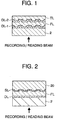
FIG. 1 is a partial cross-sectional view of the optical
information medium according to an embodiment of the present
invention.
FIG. 2 is a partial cross-sectional view of the optical
information medium according to an embodiment of the present
invention.
FIG. 3 is a partial cross-sectional view of the optical
information medium according to another embodiment of the
present invention.
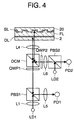
FIG. 4 is a view showing an embodiment of the optical
pickup used for recording and reading of the optical
information medium according to the present invention.
FIG. 5 is a view showing another embodiment of the optical
pickup used for recording and reading of the optical
information medium according to the present invention.
FIG. 6 is a cross-sectional view showing a step in the
formation of the transparent layer.
FIG. 7 is a cross-sectional view showing a step in the
formation of the transparent layer.
FIG. 8 is a cross-sectional view showing a step in the
formation of the transparent layer.
FIG. 9 is a cross-sectional view showing a step in the
formation of the transparent layer.
FIG. 10 is a cross-sectional view showing a step in the
formation of the transparent layer.
FIG. 11 is a cross-sectional view showing a step in the
formation of the transparent layer.
FIG. 12 is a cross-sectional view showing the medium near
the inner periphery of the substrate where the transparent
layers and the data layers have been formed.
FIG. 13 is a cross-sectional view showing a procedure for
forming the second transparent layer.
FIGS. 14A to 14D are cross-sectional views showing various
embodiments of the plug means.
The information medium to which the present invention is
applied has a structure comprising at least two
information-storing layers. The term "information-storing
layer" used herein includes both the data layer and the servo
layer. A "data layer" is the layer wherein record marks and
pits carrying the recorded information are present, and "a
servo layer" is the layer formed with a tracking servo pattern
comprising projections and depressions such as grooves and pits.
When the servo layer is not provided independently from the
data layer, tracking servo pattern may be formed on the data
layer.
In the present invention, the beam used in the reading
of the data layer and the recording of the data layer is
designated the "data beam" and the beam used in the reading
of the servo layer is designated the "servo beam". The
"recording/reading beam" of the present invention is a concept
including the data beam and the servo beam.
The "multi-layer information medium" of the present
invention is a medium comprising a plurality of
information-storing layers, and which includes an
information-storing layer whose recording and/or reading is
accomplished by the recording/reading beam which has passed
through other information-storing layer(s).
The "optical information medium" of the present invention
includes both an optical recording medium and a read only medium.
In the case of an optical recording medium, the data layer
includes a recording layer. In the case of a read only medium,
data-storing pits or record marks are preliminarily formed in
the data layer.
FIG. 1 shows an embodiment of the multi-layer medium of
the present invention in its cross section. The medium of FIG.
1 comprises a substrate 2 formed with tracking grooves, two
data layers DL-1 and DL-2 disposed on the substrate 2, a filter
layer FL between the two data layers, and a transparent layer
TL on the data layer DL-2. The transparent layer TL functions
as a protective layer. In this medium, the data layers DL-1
and DL-2 are respectively read by introducing two reading beams
each having different wavelength from the bottom side of the
medium in the drawing and detecting the reflected beam by the
optical pickup. When the medium is an optical recording medium,
the recording beam and the reading beam are generally emitted
from the same optical pickup, and the recording and the reading
beams generally have the same wavelength.
The filter layer FL of the medium of the present invention
shown in FIG. 1 exhibits an absorption for the data beam used
for reading the lower data layer DL-1 which is higher than the
absorption for the data beam used for reading the upper data
layer DL-2. As a consequence, in the reading of the data layer
DL-1, intensity of the reading beam reaching the data layer
DL-2 is reduced and the influence of the beam reflected from
the data layer DL-2 would be suppressed. In contrast, in the
reading of the data layer DL-2, the data beam is not so much
absorbed by the filter layer FL and the reading is not
obstructed. This enables provision of the data layer DL-1 and
data layer DL-2 in close proximity to each other with reduced
cross talk being induced between these data layers. In
contrast, if a transparent layer highly transparent to the
recording/reading beam were formed instead of the filter layer
FL, the optical pickup will pick the beam reflected from the
upper data layer DL-2 while the lower data layer DL-1 is read
by focusing at the lower data layer DL-1, and this will result
in a reading noise unless the thickness of the transparent layer
were fully increased.
As a matter of fact, in the reading of the upper data layer
DL-2, the influence of the beam reflected from the lower data
layer DL-1 is inescapable. The cross talk influence, however,
will be reduced when the recording density is low, and the
medium of the embodiment of FIG. 1 is preferably designed such
that the recording density of the DL-2 is lower than that of
the DL-1. In such a case, a beam with a longer wavelength is
generally used as the data beam for recording/reading of the
DL-2 compared to the data beam used for the recording/reading
of the DL-1.
FIG. 2 shows the medium according to another embodiment
of the present invention. The medium shown in FIG. 2 comprises
a substrate 2, one data layer DL on the substrate 2, a filter
layer FL on the data layer DL, and a servo substrate 20 on the
filter layer FL. The servo substrate 20 is formed with a
tracking servo pattern comprising grooves and/or pits, and on
the surface on the side of the recording/reading beam incidence
of this servo substrate 20 is formed a reflective layer which
functions as the servo layer SL.
In the reading of the medium shown in FIG. 2, a beam having
a wavelength different from the data beam used in reading the
data layer DL is used for the servo beam used in reading the
servo layer SL. The filter layer FL of this medium has an
absorption for the data beam higher than the absorption for
the servo beam, and in the reading of the data layer DL, there
is less likeliness for contamination of the reading noise
induced by the data beam reflected from the servo layer SL.
The reading of the servo information such as tracking
servo information is less likely to be influenced by the noise
compared to the reading of the data layer, and in the embodiment
shown in FIG. 2, reading of the data layer recorded at a high
recording density at low noise is realized simultaneously with
high precision servo. In addition, since the servo layer is
independently formed in the embodiment of FIG. 2, formation
of the data layer as a smooth layer is enabled. As a consequence,
the reflectivity of the data layer DL is increased, and no
interference is induced by the steps of the tracking servo
pattern. Generation of the noise due to irregularity such as
deformation of the tracking servo pattern such as winding of
the groove is also avoided. In the embodiment of FIG. 2, a
beam with a shorter wavelength is generally used for the data
beam compared to the servo beam.
FIG. 4 shows an embodiment of the optical pickup which
can be used in the recording and reading of the multi-layer
information medium of the present invention together with the
medium having the structure of FIG. 2.
In this optical pickup, the data beam is emitted from a
laser diode LD1. The data beam then goes through a lens L1
to become collimated, and after going through a polarizing beam
splitter PBS 1, the beam passes through quarter-wave plate QWP
1 and dichroic mirror DCM which is transparent to the data beam,
and the beam enters objective lens L4 to be focused at the data
layer DL of the multi-layer information medium. The data beam
reflected by the data layer DL goes back along the same pathway
as the incidence into the medium, and the beam is then reflected
by the polarizing beam splitter PBS 1 to be focused by a lens
L5 to a photodetector PD 1. The focus servo to the data layer
DL, or the focus servo and detection of the signal that has
been read is thereby accomplished.
In the medium of FIG. 4, a filter layer FL is present
between the data layer DL and the servo layer SL, and the data
beam returning to the optical pickup after being reflected at
the servo layer SL will have gone through the filter layer FL
and back to become significantly attenuated. Generation of
the noise in the reading of the data layer DL due to the
reflection at the servo layer is thereby suppressed to a
considerable degree.
In the meanwhile, the servo beam is emitted from a laser
diode LD2. The beam is then reflected by a polarizing beam
splitter PBS 2, and goes through a lens L6 and a quarter-wave
plate QWP 2 to be reflected by a dichroic mirror DCM. The beam
then enters the objective lens L4 to become focused on the servo
layer SL. The servo beam is then reflected by the servo layer
SL to go back along the same pathway as its incidence into the
medium, and the beam passes through the polarizing beam
splitter PBS 2 to be focused on a photodetector PD 2. The
tracking servo and the focus servo to the servo layer are
thereby accomplished.
Use of the optical pickup of such constitution, namely,
the optical pickup equipped with the dichroic mirror DCM which
has spectral characteristics of reflecting the servo beam while
allowing the data beam to pass therethrough is advantageous
when the data layer and the servo layer are separately provided
and the data beam and the servo beam are simultaneously
irradiated for the reading. In this way, introduction of the
reflected servo beam into the photodetector PD1 provided for
detection of the data beam as well as introduction of the
reflected data beam into the photodetector PD2 provided for
detection of the servo beam can be avoided.
The dichroic mirror DCM, however, is not capable of fully
passing the data beam therethrough, and the data beam is partly
reflected by the dichroic mirror DCM. If a transparent layer
were provided instead of the filter layer FL shown in FIG. 4,
the data beam would partly reach the photodetector PD 2 provided
for the servo purpose to adversely affect the tracking servo.
When the data beam has a high intensity as in the case of the
data beam used in the recording, such adverse effect is serious.
In contrast, when a filter layer FL is provided between the
data layer DL and the servo layer SL, the data beam is
considerably attenuated on the way and back through the filter
layer FL, and the adverse effects on the tracking servo caused
by the data beam is greatly suppressed.
FIG. 3 shows another embodiment of the multi-layer
information medium according to the present invention. The
medium of FIG. 3 comprises a substrate 2, five transparent
layers TL-1 to TL-5 on the substrate 2, and four data layers
DL-1 to DL-4 between the adjacent transparent layers. On the
transparent layer TL-5 is formed a filter layer FL, a servo
layer SL, and a servo substrate 20 in this order. The servo
substrate 20 is formed with a tracking servo pattern comprising
grooves and/or pits, and this pattern is transferred to the
servo layer SL.
The medium of FIG. 3 has a constitution similar to that
of FIG. 2 except for the larger number of data layers. When
two or more data layer are formed, and in particular, when three
or more data layers are formed, formation of the tracking servo
pattern of high precision in each of the data layer at a low
cost is difficult, and the structure wherein the data layers
and the servo layer are independently formed is effective.
In the medium of FIG. 3, the filter layer FL is provided
between the data layer DL-4 and the servo layer SL, and no filter
layer is provided between adjacent data layers. Therefore,
provision of the data layers at a close proximity invites
increase in the cross talk. When the cross talk is to be reduced
in the medium of such structure, use of an optical pickup having
a confocal optical system which utilizes the principle of a
confocal microscope is desirable. An optical pickup having
a confocal optical system has a very high resolution in the
thickness direction of the medium, and the cross talk between
the data layers can be greatly reduced by the use of such optical
pickup. Confocal optical systems which may be used in the
reading of a multi-layer information medium are described, for
example, in JP-A 222856/1998 and SOM '94 technical digest
(1994) 19.
An embodiment of the optical pickup which is equipped with
a confocal optical system and which can be used in the recording
and reading of a multi-layer information medium is shown in
FIG. 5 together with the medium. The medium shown in FIG. 5
has a structure comprising a substrate 2, and a data layer DL-1,
a transparent layer TL, a data layer DL-2, a filter layer FL,
a servo layer SL, and a servo substrate 20 disposed on the
substrate 2 in this order.
This optical pickup has a structure similar to the optical
pickup shown in FIG. 4 except that a lens L2, a pin-hole plate
PHP, and a lens L3 have been incorporated between the polarizing
beam splitter PBS 1 and the quarter-wave plate QWP1 in the light
path of the data beam.
In this optical pickup, the data beam which has passed
through the polarizing beam splitter PBS 1 is focused by the
lens L2. A pin-hole plate PHP formed with a pin hole is arranged
at the focal point, and the data beam which has passed through
the pin hole is collimated by the lens L3 and after passing
through the pathway similar to that of the optical pickup shown
in FIG. 4, the beam is focused at the data layer DL-1 on the
lower side of the multi-layer information medium. The data
beam reflected by the data layer DL-1 goes back along the same
pathway as the incidence into the medium. The data beam also
reaches the data layer DL-2 after passing through the data layer
DL-1 the data of which is to be read, and the beam is also
reflected from the data layer DL-2 back to the optical pickup.
This data beam, however, is out of focus at the data layer DL-2,
and the beam reflected from the data layer DL-2 is not focused
to the pinhole position of the pinhole plate PHP. The beam
which failed to be unfocused at the pinhole is substantially
blocked by the pinhole plate PHP. The cross talk between the
data layers is thereby suppressed by the optical pickup
equipped with the confocal optical system.
Next, constitution of various parts of the optical
recording medium of the present invention is described in
detail.
Filter layer
The filter layer shown in FIGS. 1 to 3 is a layer which
exhibits the absorption for one of the two recording/reading
beams (two data beams, or one data beam and one servo beam)
higher than the absorption for the other beam. To be more
specific, the absorption of the filter layer for one
recording/reading beam is preferably 80% or higher and more
preferably 90% or higher, and the advantage of the present
invention is not fully realized when this absorption is too
low. On the other hand, the absorption of the other
recording/reading beam is preferably 20% or lower and more
preferably 10% or lower, and when this absorption is too high,
reading of the information-storing layer by the
recording/reading beam which has gone through the filter layer
will be difficult, rendering the recording of the medium
difficult in the case of a recording medium.
The material used for the filter layer is not particularly
limited, and an adequate material may be selected from the
materials exhibiting the desired spectral absorption
characteristics, for example, from the dyes comprising an
organic material or an inorganic material. Use of an organic
dye is preferable, and use of an organic dye further comprising
a resin is more preferable. Exemplary preferable resins
include resins curable with UV or other active energy ray.
Formation of the filter layer is facilitated by such admixture
of the resin component compared to the use of the dye alone.
For example, a uniform, relatively thick filter layer can be
formed in a short period when a mixture of a UV-curable
composition an a dye is spin coated and UV cured.
The dye used for the filter layer is not particularly
limited, and an adequate dye may be selected from the dyes
exhibiting the spectral absorption characteristics required
for a filter layer, for example, from cyanine, phthalocyanine,
and azo organic dyes. The dye may be modified as desired, for
example, by introducing a substituent in the side chain of the
dye in consideration of the compatibility with the resin. The
filter layer may also comprise two or more dye layers each
having different spectral absorption characteristics for
facilitating the control of the spectral absorption
characteristics.
When the filter layer contains a dye and a resin, the dye
is not limited for its content, and the content may be
determined depending on the type of the resin employed and to
satisfy the required spectral absorption characteristics.
The content is typically 1 to 10 mass%. An excessively low
dye content is undesirable since increase in the thickness of
the filter layer is required. On the other hand, excessively
large content will result in the shortening of the pot life.
When the wavelength of the beam to be absorbed is
relatively short, and to be more specific, when steep
absorption is to be realized in the wavelength region of up
to 450 nm, the filter layer may be constituted from a UV-curable
resin layer free from the dye. The UV-curable resin layer may
be formed by coating a composition containing a UV-curable
composition and a photoinitiator, and UV curing the coated film.
The photoinitiator exhibits high absorption near the
wavelength of the light beam used for the curing, and the thus
cured film also exhibits high absorption near such wavelength.
This is believed to be due to the condition that the
photoinitiator is not completely decomposed in the course of
curing and a part of the photoinitiator remains in intact or
modified state after the curing. As a consequence, such layer
can be used as a filter layer which exhibits selectively high
absorption at the short wavelength region.
The photoinitiator used in the filter layer is not
particularly limited, and an adequate photoinitiator may be
selected from conventional photoinitiators such as benzoates,
benzophenone derivatives, benzoin derivatives, thioxanthone
derivatives, acetophenone derivatives, propiophenone
derivatives, and benzyls depending on the wavelength of beam
to be absorbed.
The thickness of the filter layer may be adequately
determined to satisfy the required spectral absorption
characteristics. However, the filter layer containing a resin
wherein a dye or a photoinitiator is used for the absorption
material is preferably formed to a thickness in the range of
1 to 30 µm. When the filter layer is too thin, sufficient
absorption characteristics is less likely to be obtained.
When the filter layer is too thick, number of the data layers
included in the medium will be limited in view of the total
thickness of the medium, and this is not preferable.
When the wavelength of the beam to be absorbed is
relatively short, for example, up to 450 nm, a metal layer
containing at least one metal (including semimetal) element
may be used for the filter layer. Some metals including gold
exhibit steep high absorption in the short wavelength region.
In view of such situation, the type of the metal included and
the thickness of the filter layer may be selected so that
sufficient absorption and sufficient transmittance are
reliably achieved at the target wavelength regions of
absorption and transmittance, respectively. Examples of the
metals which may be preferably used in the filter layer include
Au, Pt, Cu and the like. The filter layer may also comprise
two or more different metal layers each having different
spectral absorption characteristics.
The thickness of the metal layer used as the filter layer
may vary by the type of the metal used. However, the thickness
of such layer is preferably in the range of 10 to 200 nm, and
more preferably 20 to 100 nm. When the metal layer is too thin,
the layer will fail to exhibit sufficient absorption at the
target absorption wavelength region while excessively thick
metal layer results in an insufficient transmittance at the
target wavelength region.
The filter layer may also comprise an interference filter.
Exemplary interference filters which may be used include a
dielectric multi-layer film and a dielectric layer sandwiched
between two metal thin films comprising Ag or the like.
In the embodiment of FIG. 3, the filter layer is provided
only between the data layer and the servo layer, namely, only
at one of the locations between the adjacent information-storing
layers. The filter layer, however, may be also formed
at other locations between adjacent information-storing
layers as desired. To be more specific, two or more filter
layers may be formed with three or more beams each having
different wavelength being used for the recording or reading
beam. For example, data layers DL-1, DL-2, and DL-3 may be
formed in this order from the side of the light incidence with
filter layers FL-1 and FL-2 respectively formed between the
DL-1 and the DL-2 and between the DL-2 and the DL-3, and the
DL-1, the DL-2 and the DL-3 may be read with the beams having
a wavelength of 400 nm, 600 nm and 800 nm, respectively. In
this case, the filter layer FL-1 is preferably the one
exhibiting high absorption to the beam with a wavelength at
around 400 nm and low absorption to the beams at around 600
nm and 800 nm. The filter layer FL-2 is not limited for its
absorption for the beam with the wavelength at around 400 nm
while it should exhibit high absorption at around 600 nm and
low absorption at around 800 nm.
To be more specific, in the case of a medium wherein the
number of the filter layers is "n" and which is to be used in
a system wherein "n+1" recording/reading beams each having
different wavelengths are used, the filter layer should exhibit
a relatively high absorption for the reading/recording beam
used for its closest information-storing layer on the side of
the light incidence and a relatively low absorption for the
reading/recording beam used for its closest information-storing
layer on the side of the light exit. The "relatively
high absorption" used herein designates an absorption of
preferably 80% or higher, and more preferably 90% or higher,
and the "relatively low absorption" used herein designates an
absorption of preferably 20% or lower, and more preferably 10%
or lower.
When two or more filter layers are formed, all of the
filter layers may not necessarily comprise the same type of
optical absorbing material. The filter layers, for example,
may comprise a combination of a metal layer or an interference
filter and a dye-containing filter layer.
In the medium of FIG. 3, the reflective layer (the servo
layer SL) on the surface of the servo substrate 20 may be used
as the filter layer instead of forming a filter layer between
the data layer and the servo layer. In the case when the present
invention is used in a read only medium, the transparent layer
or the filter layer may be formed with pits, and a translucent
reflective layer may be formed on the surface formed with the
pits by sputtering or the like to thereby use the thus formed
reflective layer also as the data layer. In this case, the
reflective layer formed from a metal or a semi-metal may be
used as the filter layer. In such case, the filter layer which
also serves as the information-storing layer may preferably
exhibit a relatively high reflectivity for the
recording/reading beam used for the filter layer itself and
a relatively low reflectivity for the recording/reading beam
used for its closest information-storing layer on the side of
the light incidence. If an information-storing layer is also
present on the side of the light exit, the filter layer may
preferably exhibit a relatively high transmittance for the
recording/reading beam used for such information-storing
layer.
The recording/reading beams having different wavelengths
from each other are not particularly limited for their
wavelengths. However, difference in the wavelength between
these recording/reading beams is preferably in the range of
50 to 700 nm, and more preferably 100 to 400 nm. When the
wavelength difference is too small, the filter layer will be
required to have steep spectral absorption characteristics and
selection of the material used for the filter layer will be
difficult. When the wavelength difference is too large,
difficulty is encountered in increasing the recording density
of the entire medium or in obtaining sufficient servo accuracy.
The wavelength region wherein these recording/reading
beams are present is preferably the wavelength region of 300
to 1000 nm, and more preferably 400 to 800 nm. A semiconductor
laser oscillating a laser beam having a wavelength shorter than
such range is difficult to obtain while use of a laser beam
having a wavelength longer than such range is associated with
difficulty in high density recording as well as difficulty in
the reading of the information recorded at a high density.
Transparent layer
The transparent layer in FIG. 3 preferably comprises a
material which exhibits high transmittance to the
recording/reading beam. The material used for the transparent
layer is not limited. The transparent layer, however, is
preferably formed from a resin since the transparent layer
should be deposited to a considerable thickness. The process
used for the formation of the transparent layer is not limited.
In view of the ease of forming a uniform, transparent layer
in short time, the transparent layer is preferably formed from
a resin, and in particular, from a UV-curable resin or other
active energy beam-curable resin. It should be noted that the
transparent layer may be also formed from a resin sheet.
When the transparent layer is provided in contact with
the substrate 2, it should be noted that the difference between
the refractive index of the transparent layer and the
refractive index of the substrate is up to 0.1 at the wavelength
of the recording/reading beam in order to suppress the
reflection at the boundary between the transparent layer and
the substrate.
The transparent layer formed from a UV-curable resin will
exhibit a relatively steep absorption in the short wavelength
region due to the influence of the photoinitiator as described
above in the section of the "Filter layer". In order to
reliably impart the transparent layer with a sufficient
transparency to the recording/reading beam in the short
wavelength region, an adequate type of photoinitiator should
be selected depending on the wavelength of the
recording/reading beam used.
The transparent layer is not particularly limited for its
thickness, and the thickness may be adequately determined so
that the cross talk between the data layers is within acceptable
limits. Typically, the transparent layer has a thickness of
at least 30 µm when an optical pickup of conventional type is
used. An excessively thick transparent layer is likely to
result in an unduly increased inconsistency in the thickness
as well as increased internal stress, and such a thick
transparent layer is also likely to invite increase in the total
thickness of the medium. Accordingly, the transparent layer
preferably has a thickness of up to 100 µm.
On the other hand, when a confocal optical system is
adopted, the thickness of the transparent layer is determined
depending on the resolution of the confocal optical system in
the depth direction so that the cross talk between the data
layers is within acceptable limits. To be more specific, the
preferable thickness of the transparent layer is 5 µm or more
when the data beam has a wavelength of about 300 to about 1000
nm although such thickness may vary with the wavelength of the
data beam and the constitution of the confocal optical system.
Use of a confocal optical system enables provision of a
transparent layer with a reduced thickness of less than 30 µm,
and no problem is induced even when the thickness is reduced
to 20 µm or less.
When the medium has a disk shape and the transparent layer
comprises a resin, the transparent layer is preferably formed
by spin coating since the spin coating is a process which is
capable of forming a relatively uniform transparent layer. In
the transparent layer formed by spin coating, however, the
radially outer portion of the resin layer becomes thick in
relation to the radially inner portion of the layer, and the
transparent layer would suffer from an increased thickness
inconsistency in radial direction. The number of the
transparent layers increases with the number of the data layers,
and such thickness inconsistency is accumulated with the
increase in the number of the data layers. As a consequence,
even if the data beam entered the substrate 2 in the outer
peripheral region of the disk at normal direction, the data
beam reflected at the surface of the data layer will not be
normal to the substrate 2, and the quantity of the light
returning to the optical pickup will be reduced. The medium
will then exhibit different reading outputs in the inner
peripheral region and in the outer peripheral region.
In the case of an optical pickup equipped with a confocal
optical system, a pinhole is provided in the optical system
and the reading is accomplished by using the beam that had
passed thorough this pinhole. Accordingly, when an optical
pickup equipped with a confocal optical system is used, the
range of the focus servo will be narrower, and therefore, a
higher thickness consistency is required for the transparent
layer.
In view of such situation, difference between the maximum
thickness and minimum thickness of the transparent layer
between recorded information-storing areas (area where the
recording tracks are present) of two adjacent data layers or
between the recorded information-storing area of the data layer
and the servo information-storing areas of the servo layer is
preferably up to 3 µm, and more preferably up to 2 µm. When
the thickness inconsistency of the transparent layer is reduced
to such range, the fluctuation in the reading output can be
critically reduced. Although it may be preferable that the
difference between the maximum and minimum thickness of the
transparent layer is reduced to the lowest possible value,
reduction of such difference to zero is difficult as long as
the transparent layer is formed by spin coating, and the
fluctuation in the reading output is sufficiently reduced when
the thickness difference is within the above-specified range.
Therefore, the thickness difference need not be reduced to less
than 1 µm. In the disk-shaped medium, the recorded
information-storing area is typically an annular area having
a width of about 20 to about 50 mm.
It should be also noted that the resin layers other than
the transparent layer, for example, the filter layer comprising
a resin or a resin and a dye, a protective layer which is often
provided on the surface of the medium, an adhesive layer, and
the like may be formed by spin coating. These resin layers
are also required to have reduced thickness inconsistency as
in the case of the transparent layer.
In order to reduce the thickness inconsistency of the
transparent layer, the filter layer, and other resin layers,
the step of the spin coating is preferably accomplished by using
the apparatus as described below.
The step of the spin coating is explained in the following
by referring to an example wherein the transparent layer TL-1
is formed in the medium of FIG. 3. In this method, a substrate
2 formed with a center hole 101 is placed on a turntable 200
as shown in FIGS. 6 and 7. It should be noted that, when a
transparent layer other than the TL-1 is formed, the substrate
2 has an information-storing layer or an information-storing
layer and a resin layer already formed thereon. The substrate
2 is secured to the turntable 200 with its center hole 101 fitted
on an annular ridge 201 of the turntable 200. FIGS. 6 and 7
are cross-sectional views showing only the end faces appearing
at the section, and the views in depth direction are omitted.
This also applies to the following cross-sectional views.
Next, the center hole 101 is covered with a plug means
300. The plug means 300 has a disk member 301 for covering
the center hole 101, a support shaft 302 integrally formed with
the disk member 301 at its center, and a projection 303
integrally formed with the disk member 301 on the side facing
the center hole 101. By fitting the projection 303 inside the
ridge 201, the plug means 300 is secured to the turntable 200
and the substrate 2 can be positioned in relation to the plug
means 300. The method used in securing the substrate 2 and
the plug means 300 to the turntable 200 is not particularly
limited, and in an exemplary method, the substrate 2 is first
fitted with the plug means 300, and the plug means 300 is then
fitted in the turntable 200.
Next, a coating solution 500 comprising a resin or a resin
solution is poured as shown in FIG. 8 from a nozzle 400 which
is a discharging means to deliver the coating solution 500 to
the outer periphery of the support shaft 302. The turntable
200 is simultaneously rotated at a relatively low speed, and
preferably at a rotation speed of 20 to 100 rpm so that the
coating solution is uniformly distributed over the disk member
301.
Next, the turntable 200 is rotated at a relatively high
speed to spread the coating solution 500 on the substrate 2
as shown in FIG. 9 and to thereby form the transparent layer
TL-1 on the substrate 2.
The conditions used for the spreading of the coating
solution are not particularly limited. It is known that the
thickness of the coated film theoretically increases in
relation to the square root of the coating solution viscosity
if the spin coating is conducted such that the conditions other
than the coating solution viscosity are identical. On the
other hand, the coated film becomes thin with the increase in
the rotation speed and the rotation time. Therefore, the
rotation speed and the rotation time used in the spin coating
may be adequately determined depending on the thickness of the
transparent layer TL-1 to be formed and the coating solution
viscosity.
Next, the plug means 300 is separated from the substrate
2 as shown in FIG. 10. As the outer periphery of the disk member
301 leaves the substrate 2, the inner periphery of the
transparent layer TL-1 is lifted, and an annular raised rim
600 is formed as shown in FIG. 10. The annular raised rim 600
is the portion wherein the resin constituting the transparent
layer TL-1 is continuously uplifted.
When the coating solution used contains a UV-curable resin,
the transparent layer TL-1 is cured by UV irradiation as shown
in FIG. 11. Although the UV irradiation is conducted in FIG.
11 on the turntable 200, the curing may also be conducted on
a curing stage separately provided from the turntable. Also,
the separation of the plug means may be accomplished while the
substrate is rotated.
The annular raised rim 600 formed by such method has a
cross section of smooth curve (arc) as shown in the drawings.
On the contrary, if the plug means 300 is separated after the
curing of the transparent layer TL-1, a continuous annular
raised rim will not be formed, and even if some projections
were formed at the corresponding position, the projections
formed will be burrs and not an annular raised rim continuously
extending in peripheral direction. Such procedure also
involves the problem that debris of the cured resin are likely
to scatter over the substrate 2.
Height of the annular raised rim 600, namely, height of
the top of the annular raised rim measured from the lowest part
in the surface of the resin layer near the annular raised rim
is typically in the range of 1 to 100 µm. Width of the annular
raised rim 600, namely, distance between the lowest part in
the surface of the transparent layer near the annular raised
rim to the inner periphery of the transparent layer is typically
in the range of 0.5 to 3 mm. It should be noted that the height
and the width of the annular raised rim increases with the
increase in the thickness of the resin layer.
After completing the formation of the first transparent
layer TL-1, first data layer DL-1 is formed by means of
sputtering or the like. The data layer is formed such that
the inner periphery of the data layer is located at a position
radially outside the inner periphery of the underlying
transparent layer.
Next, a second transparent layer TL-2 is formed by using
the plug means 300 again. This time, the annular raised rim
600 is already present at the inner periphery of the first
transparent layer TL-1. If the plug means 300 used is the same
as the one used in the formation of the TL-1, spreading of the
resin will be inhibited by the annular raised rim 600 and
formation of the TL-2 is likely to be interfered. In addition,
the annular raised rim formed in TL-2 will be formed over the
annular raised rim of the TL-1 to result in great deviation
of the resin layer thickness near the disk inner periphery from
the designed value, and the distance between the data layers
will be increased in the region near the inner periphery.
In order to solve such problem, the resin layers are formed
in the present invention such that the annular raised rims of
the resin layers are located in mutually displaced relationship.
FIG. 12 is a cross-sectional view of the substrate 2 near its
inner periphery wherein the transparent layers TL-1 to TL-4
and the data layers DL-1 to DL-4 have been alternately
disposed. In FIG. 12, the transparent layer remote from the
substrate 2 has a larger inner diameter, and as a consequence,
the inner periphery of the transparent layer laminate after
the formation of the transparent layers has a step-like
configuration, and the annular raised rims 600 are left exposed
on the surface of the thus formed steps. As described above,
the problem as described above can be solved by disposing the
transparent layers in the form of steps so that the subsequently
formed transparent layer does not cover the annular raised rim
of the preceding transparent layer.
In order to form a transparent layer laminate having the
inner periphery of step-like configuration, the second
transparent layer TL-2 may be formed by using a plug means 300
as shown in FIG. 13. The procedure shown in FIG. 13 is
substantially the same as the procedure shown in FIG. 6 except
for the use of the substrate 2 which is already formed with
the transparent layer TL-1. The plug means 300 used, however,
is different. The disk member 301 of this plug means 300 has
a diameter larger than the one shown in FIG. 6 in order to form
a transparent layer having an inner diameter larger than the
transparent layer TL-1. The disk member 301 is also bored in
its lower surface so that the member will be in contact with
the flat area of the transparent layer TL-1 by bridging the
annular raised rim 600. The third and the following
transparent layers may be formed by using a plug means having
a disk member of similar configuration but of the size which
can cover the annular raised rim of the preceding transparent
layer.
The plug means used in the procedure as described above
is not limited for its constitution as long as its includes
a disk member for blocking the center hole of the disk substrate.
Spin coating methods using a plug means for blocking the center
hole of the disk substrate are described, for example, in JP-A
320850/1998, JP-A 249264/1998, JP-A 289489/1998, JP-A
195250/1999, and JP-A 195251/1999. These documents disclose
methods wherein the center hole of the disk is blocked with
a plug means such as a plate-shaped substrate, a disk member,
a plug member, or a cap, and the resin is supplied to a location
near the center of such plug means, namely, near the rotation
center to thereby reduce the thickness unevenness in radial
direction of the resin layer. However, these documents refer
neither to the multi-layer information medium nor to the
formation of annular raised rim at the inner periphery of the
resin layer in the spin coating. In addition, the plug means
described in these documents suffer from the problems as
described below.
Of these documents, JP-A 320850/1998, JP-A 249264/1998,
and JP-A 195250/1999 do not disclose removal of the plug means,
namely, the plate-shaped member or the cap after the spin
coating, and employment of such methods in an industrial
production is difficult. These documents are also silent
about the curing of the resin layer after the separation of
the plug means from the disk substrate.
JP-A 289489/1998 discloses curing of the resin layer while
rotating the disk substrate after the spin coating and removal
of the plate-shaped member, namely, the plug means by knocking
or electromagnetic suction. The removal of the plug means by
knocking or electromagnetic suction, however, applies a
considerable acceleration to the plug means, and this is likely
to cause turbulence in the resin coating film.
JP-A 195251/1999 discloses a plug means comprising a
spherical cap and a support member integrally formed with the
spherical cap at its center. JP-A 195251/1999 teaches that
this support member facilitates the attachment/detachment and
the positioning of the plug means. The support member of JP-A
195251/1999 comprises either a hollow cylinder provided with
at least one opening or a plurality of rods. The resin layer
is formed on the disk substrate by introducing the resin into
the interior of the hollow cylinder or into the area surrounded
by the plurality of rods, and rotating the disk substrate
together with the plug means. These plug means certainly
facilitate removal of the plug means. JP-A 195251/1999
discloses curing of the resin layer in stationary state after
separating the plug means from the disk substrate.
In JP-A 195251/1999, the spin coating is accomplished by
allowing the resin to flow from the openings provided on the
hollow cylinder of the plug means or from the intervals between
adjacent rods of the plug means. Therefore, the resin is once
stopped at the wall (i.e. area of the wall other than the
opening) or rods of the support member, and the stopped resin
may sweep onto the disk substrate at an unexpected timing to
result in an uneven coating. In addition, these plug means
are difficult to clean since the part that becomes in contact
with the resin is quite complicated in shape and a large area
is brought in contact with the resin. The resin remaining on
the plug means may become a cause of an uneven coating.
Furthermore, as shown from the results of Table 1 in JP-A
195251/1999 wherein variation of the coating thickness is shown
in relation to the outer diameter of the hollow cylinder of
from 4 to 16 mm, the unevenness of the thickness depends on
the outer diameter of the hollow cylinder, and the degree of
the coating unevenness increases with the increase in the outer
diameter of the hollow cylinder. To be more specific, even
when the resin is supplied to the interior of the hollow
cylinder, the starting point of the coating will be deviated
from the center of rotation, and the starting point of the
coating will be the position where the outer periphery of the
hollow cylinder is located. In consideration of the
relatively high viscosity of the resin, the outer diameter of
the hollow cylinder can not be reduced to below 4 mm. Therefore,
the thickness unevenness of the resin coating is difficult to
reduce by the method described in JP-A 195251/1999.
In contrast to such conventional plug means, the plug
means 300 shown in FIG. 6 comprises a disk member 301 and a
support shaft 302 provided thereon. Therefore, handling of
the plug means 300 in the production of the medium is easy,
and in particular, removal of the plug means 300 after spin
coating is facilitated.
JP-A 195251/1999 discloses a plug means constituted from
a cap and a support member comprising a hollow cylinder or a
plurality of rods integrally formed with the cap. The plug
means shown in FIG. 6 has various advantages over such plug
means as described below.
In JP-A 195251/1999, the resin is once blocked at the wall
or rods of the support member, and this may cause an uneven
coating as described above. In contrast, in the plug means
shown in FIG. 6, the spin coating is accomplished by supplying
the coating solution on the outer periphery of the support shaft
and the thickness evenness is unlikely to be induced. In
addition, in the case of the plug means shown in FIG. 6, the
part to which the resin attaches is the outer periphery of the
support shaft, and cleaning of the plug means is easy compared
to JP-A 195251/1999. Furthermore, the coating solution is
supplied in JP-A 195251/1999 to the interior of the hollow
cylinder and the outer diameter of the support member can not
be reduced below certain level if the mobility of the coating
solution with relatively high viscosity is to be ensured, and
accordingly, the starting point of the coating is relatively
remote from the center of rotation. In contrast, the outer
diameter of the support shaft of the plug means shown in FIG.
6 can be reduced to a value significantly smaller than that
of JP-A 195251/1999, and the thickness unevenness of the
coating can be markedly reduced compared to JP-A 195251/1999.
It should be noted that such advantages are realized not
only by the plug means constituted as shown in FIG. 6, and as
long as the plug means is constituted from a disk member and
a support shaft, the advantages may be realized. The plug means
300 shown in FIG. 6 comprises a frustoconical disk member 301
and a columnar support shaft 302. Other embodiments of the
plug means which may be adopted include those having the
structures as shown in FIGS. 14A to 14D.
The plug means shown in FIG. 14A comprises a frustoconical
disk member 301 having bored lower surface as in the case of
FIG. 13 and an inverted frustoconical support shaft 302. When
such plug means is used, the starting point for the coating
of the coating solution can be brought nearer to the center
of the disk member 301 to further reduce the thickness
unevenness of the coated layer. In addition, provision of such
support shaft 302 is not associated with decrease in its
mechanical strength in contrast to the case wherein the
diameter of the entire support shaft 302 is reduced.
Furthermore, the plug means of such configuration is
advantageous in attaching/detaching and carrying of the plug
means since gripping of the support shaft 302 with a chuck and
the like is facilitated to avoid dropping. It should be noted
that not the entire support shaft 302 needs to be inverted
frustoconical. To be more specific, at least a part of the
support shaft 302 should be frustoconical with its diameter
reducing toward the disk member 301 and the remaining portion
of the shaft on the side of the disk member may not necessarily
be tapered as long as the diameter does not increase toward
the disk member.
The plug means shown in FIG. 14B is different from the
one shown in FIG. 14A in its cross-sectional configuration of
the disk member 301. In order to facilitate consistent
spreading of the coating solution on the disk member 301, the
disk member 301 may preferably have a thickness gradually
decreasing toward its outer periphery. In such case, the upper
surface where the coating solution spreads may have a
rectilinear cross section as shown in FIG. 14A or a curved cross
section as shown in FIG. 14B. In addition, the disk member
301 may have a vertical outer periphery as shown in FIG. 14C,
and in such as case, the thickness t of the disk member 301
at its periphery is preferably up to 0.4 mm since even coating
of the resin layer is difficult at an excessively large
thickness t. The disk member 301 may also have an even
thickness as shown in FIG. 14D.
The plug means shown in FIGS. 14A to 14D are those wherein
lower surface of the disk member 301 has been bored to
correspond to the formation of the second or the following resin
layer.
In the plug means, the minimum diameter of the support
shaft 302 near the disk member 301 is preferably less than 4
mm, and more preferably 2 mm or less. When the diameter of
the support shaft 302 near the disk member 301 is too large,
the starting point of the coating will be remote from the center
of the disk member 301 to invite an increase in the thickness
unevenness in the radial direction of the resin layer. When
the diameter of the support shaft 302 near the disk member 301
is too small, the support shaft 302 will suffer from
insufficient mechanical strength. Therefore, the minimum
diameter is preferably at least 0.5 mm, and more preferably
at least 0.7 mm. The support shaft 302 is not limited for its
length, and an adequate length may be selected by taking ease
of supplying the coating solution to the outer periphery, ease
of the gripping and the like into consideration. The length
of the support shaft, however, is preferably in the range of
5 to 100 mm, and more preferably 10 to 30 mm. An excessively
short support shaft 302 is associated with difficulty in
supplying the coating solution to its outer periphery as well
as difficulty in the gripping. In contrast, an excessively
long support shaft 302 suffers from handling inconvenience.
The diameter of the disk member 301 is not limited as long
as it is larger than the diameter of the center hole 101 of
the disk substrate and smaller than the inner diameter of the
annular information recording area of the disk substrate. The
diameter of the disk member 301, however, is preferably at least
4 mm, and more preferably at least 8 mm larger than the diameter
of the center hole 101 in consideration of the risk of the
coating solution 500 going underneath the disk member 301 onto
the periphery of the center hole 101 (inner periphery of the
disk substrate). The diameter of the disk member 301 is
preferably at least 3 mm, and more preferably at least 5 mm
smaller than the inner diameter of the information recording
area since the configuration of the resin layer near the disk
member 301 may be affected by the removal of the disk member
301. Although the diameter of the disk member 301 employed
may vary according to the diameter of the center hole and the
inner diameter of the information recording area, the diameter
of the disk member 301 is typically in the range of 20 to 40
mm, and preferably 25 to 38 mm when the optical disk has a
diameter of about 60 to 130 mm.
The material used for constituting the plug means is not
particularly limited and the material may be a metal, a resin,
a ceramics, or a composite material containing two or more such
materials. The disk member 301 and the support shaft 302 may
also comprise different materials. In view of the mechanical
strength, durability, and dimensional precision, the plug
means preferably comprises a metal. Exemplary preferable
metals include stainless steel alloy, aluminum, and aluminum
alloy.
Surface tension of the surface of the plug means 300, and
in particular, the entire surface of the disk member 301 is
preferably lower than that of the coating solution. When the
surface of the plug means 300 is less wettable to the coating
solution, removal by washing of the coating solution that has
attached to the surface of the plug means will be facilitated.
The surface tension of the plug means can be controlled by
adequately selecting the material used for the plug means.
However, it is more preferable that the area where surface
tension is to be reduced is subjected to a water- and oil-repellent
treatment such as treatment with teflon.
Servo layer
The servo layer is a reflective layer formed on the servo
substrate 20, and the servo layer is formed with the projections
and depressions carrying the tracking servo information. The
servo layer carries tracking servo information corresponding
to the projections and depressions. Grooves and/or pits are
typically used for the projections and depressions.
The reflective layer constituting the servo layer is not
particularly limited for its constitution, and the reflective
layer formed may be similar to those formed in conventional
optical information media. The reflective layer may typically
comprise a metal or semimetal such as Al, Au, Ag, Pt, Cu, Ni,
Cr, Ti, or Si as a simple substance or as an alloy containing
at least one of such metals and semimetals. The reflective
layer is typically formed to a thickness of 10 to 300 nm. A
thickness below such range is likely to result in an
insufficient reflectivity while the thickness in excess of such
range is not advantageous in cost since increase in the
thickness does not result in significant increase of the
reflectivity. The reflective layer is preferably formed by
vapor deposition such as sputtering and evaporation.
Data layer
When the present invention is applied to an optical
recording medium, the data layer includes at least a recording
layer comprising a recording material. The optical recording
medium to which the present invention is applied is not limited
particular type, and applicable media include a rewritable
medium or a write once medium employing a phase change recording
material, a rewritable medium employing a magnetooptical
recording material, a write once medium employing an organic
dye. However, use of a phase change recording material is
preferable in view of high light transmittance compared to
other recording materials, and accordingly, capability of
increasing the number of recording layers.
The composition of the phase change recording material
is not particularly limited, and the material is preferably
the one containing at least Sb and Te. However,
crystallization temperature of the recording layer containing
Sb and Te as the only components is as low as about 130°C and
the storage reliability is insufficient, and therefore, the
recording layer may preferably comprise elements other than
Sb and Te. Such element is preferably element M (element M
is at least one element selected from In, Ag, Au, Bi, Se, Al,
P, Ge, H, Si, C, V, W, Ta, Zn, Ti, Ce, Tb, Sn, Pb, Pd, and Y),
and among these, the preferred is Ge in view of the high effect
in improving the storage reliability.
When the atomic ratio of the elements constituting the
recording layer is represented by the formula (I):
SbaTebMc
wherein a+b+c = 1, a, b, and c are preferably such that:
0.2 ≤ a ≤ 0.85,
0.1 ≤ b ≤ 0.6,
and
0 ≤ c ≤ 0.25,
and more preferably,
0.01 ≤ c ≤ 0.25.
When the content of Sb is too low, crystallization speed will
be insufficient and the overwriting will be difficult. On the
other hand, when the Sb content is too high, crystallization
speed will be excessively high and formation of amorphous
record marks will be difficult. When the content of M is too
low, the effect of M addition will be insufficient while
addition of M in an excessive amount will result in insufficient
alteration of the reflectivity with the phase change, and hence,
in an insufficient degree of modulation. When Te content is
too low, formation of record marks will be difficult due to
the difficulty in amorphization. On the other hand, when the
Te content is too high, crystallization speed will be
insufficient and overwriting will be difficult.
A phase change recording medium is generally used as a
rewritable medium. In the present invention, however, the
phase change recording medium may be used as a write once medium.
The "write once medium" used herein designates a medium which
is recordable but wherein erasure of the once recorded record
mark is not ensured, and in the case of a write once medium,
overwriting of the record marks recorded in the recording track
by erasing the record marks is not intended. Advantages
associated with the use of a phase change recording medium for
the write once medium are as described below.
In the case of a multi-layer recording medium, a plurality
of recording layers are disposed one on another, and this
structure is accompanied with an increased loss in the light
quantity of the recording/reading beam. Therefore, use of a
thinnest possible recording layer is desired. Decrease in the
thickness of the recording layer, however, invites an increase
in the cooling speed of the recording layer after the recording
beam irradiation. Crystallization is less likely to take
place at a higher cooling speed, and use of a composition which
easily undergo crystallization is required to ensure the
erasability. In other words, considerable increase in the
crystallization speed of the recording layer will be required.
A recording layer of high crystallization speed, however, is
associated with the problem of higher occurrence of the self
erase as described below. In the recording, heat dissipates
from the beam spot of the recording beam in the lateral
direction of the recording layer, and cooling of the record
marks is inhibited by this heat. When the recording layer has
a high crystallization speed, the record marks are partly
recrystallized due to such cooling inhibition, and the size
of the record mark formed will be reduced. To be more specific,
the phenomenon often encountered is erasure of the leading edge
of the record mark (the part first irradiated with the beam
spot) or the trailing edge of the record mark. Such phenomenon
is referred in the present invention as the "self erase". The
self erase is associated with decrease in the C/N or increase
in the jitter.
As described above, when the thickness of the recording
layer is reduced, it will be difficult to simultaneously ensure
sufficient erasability and suppress the self erase. In
contrast, when a medium having a phase change recording layer
is used as a write once medium, there will be no need to erase
the record marks, and hence, to consider the crystallization
speed of the recording layer. Accordingly, no problem will
be induced even if the crystallization speed of the recording
layer were reduced to the level where no substantial influence
on the self erase is induced. In addition, when overwriting
is conducted, increase in the crystallization speed of the
recording layer is required with the increase in the linear
velocity of the medium in the recording, and this also invites
increased likeliness of self erase. However, if the recording
is conducted only once with no overwriting operation, it will
be possible to conduct the recording at a high linear velocity,
for example, at a linear velocity of about 10 m/s in a recording
layer having a relatively slow crystallization speed with
reduced likeliness of self erase, and a high data transfer rate
is easily realized.
As described above, the medium of the present invention
has a plurality of recording layers disposed one on another
and loss of the light quantity of the recording/reading beam
is accordingly increased. Therefore, use of a thinnest
possible recording layer is preferable with the function of
the recording layer maintained. However, an excessively thin
recording layer can no longer function as a recording layer,
and the recording layer preferably has a thickness of 2 to 50
nm, and more preferably, 4 to 20 nm.
When a phase change recording layer is employed, the data
layer may preferably have the structure as shown for DL-1 in
FIG. 3. This data layer has a structure wherein the recording
layer 4 is sandwiched between the first dielectric layer 31
and the second dielectric layer 32. When such structure is
adopted, the recording layer and the dielectric layers are
preferably formed by sputtering. The dielectric material used
in the dielectric layers may be a compound containing at least
one metal component selected from Si, Ge, Zn, Al, and rare earth
metals, and the compound is preferably an oxide, a nitride,
a sulfide, or a fluoride. A mixture containing two or more
such compounds may be also used. Each dielectric layer may
preferably have a thickness of 10 to 500 nm.
In the structure shown in FIG. 1, the data layer DL-2 which
is the furthest data layer from the side of the
recording/reading beam incidence generally comprises a
laminate of the reflective layer, the dielectric layer, the
recording layer, and the dielectric layer disposed in this
order from the upper side of the drawing. On the other hand,
no reflective layer is formed in the case of the data layer
DL-1 of FIG. 1 to facilitate the transmittance of the
recording/reading beam therethrough. However, the data layer
DL-1 may optionally include a reflective layer which is
translucent to the recording/reading beam, and in such a case,
the data layer DL-1 will have a structure similar to that of
the data layer DL-2.
In the present invention, use of the recording layer with
a reduced thickness is preferable in order to reduce the loss
in the light quantity of the recording/reading beam. Decrease
in the thickness of the phase change recording layer, however,
is associated with a decrease in the degree of modulation,
namely, with a decrease in the difference in reflectivity
between the amorphous record mark and the crystalline region.
In order to increase the degree of modulation, the dielectric
layer is preferably formed as a laminate of two or more layers
each having different refractive index. Such multi-layer
structure also results in an increased flexibility of optical
design, and increase in the light transmittance of the entire
data layer can be realized. An exemplary dielectric layer of
multi-layer structure is a laminate of at least one layer
selected from magnesium fluoride layer, manganese fluoride
layer, germanium nitride oxide layer, and silicon oxide layer
with a ZnS-SiO2 layer.
When a plurality of recording layers are formed, intensity
of the recording beam reaching the particular recording layer
reduces with the increase in the distance of the recording layer
from the surface of the recording beam incidence into the medium.
Therefore, recording sensitivity of the recording layer is
preferably adjusted corresponding to the intensity of the
recording beam reaching to the particular recording layer. In
the case of recording materials wherein heat mode recording
is conducted as in the case of phase change recording materials,
increase in the thickness of the recording layer results in
an increase in heat storage, and hence, in an increase in the
recording sensitivity. In view of such situation, the
thickness of the recording layer remote from the surface of
the recording beam incidence may be increased as required
compared to the recording layer near the surface of the
recording beam incidence. However, adjacent two recording
layers may have an identical thickness. In addition, the
recording/reading beam used in the recording layer remote from
the surface of the recording beam incidence is the
recording/reading beam which has passed through other
recording layers, and for the purpose of leveling the reading
properties of the recording layers, a recording layer near the
surface of the recording beam incidence may preferably have
a higher light transmittance. In consideration of such light
transmittance, it is also preferable that the recording layer
remote from the surface of the recording beam incidence has
an increased thickness.
It should be noted that the adjustment of the recording
sensitivity and the transmittance can also be accomplished
through control of the composition of the recording layer. In
such case, all recording layers may be formed to an identical
thickness, or alternatively, control of the composition can
be combined with the control of the thickness.
The present invention is also applicable to a read only
medium. The data layers of such medium may comprise either
a layer formed with pits carrying the recorded information or
a layer of a write once medium carrying the preliminarily
recorded data. In the former case, the pits are generally
formed in the transparent layer or the filter layer, and a
translucent reflective layer is formed on the surface of the
layer formed with the pits. The reflective layer will then
serve as the data layer. Examples of such translucent
reflective layers are an extremely thin metal layer and a
silicon layer. In such read only medium, reflectivity of the
data layer may be controlled for the leveling of the readout
signal. To be more specific, the reflectivity may be
controlled such that the data layer with the smaller quantity
of light reached exhibits higher reflectivity. When the
reflectivity is controlled as described above, the data layer
near the surface of the beam incidence will exhibit higher light
transmittance and marked attenuation in the quantity of the
light reaching the data layer remote from the surface of the
beam incidence will be avoided.
In the present invention, number of the data layers
included in the medium is not limited as long as two or more
data layers are included. An excessive number of data layers,
however, results in unduly increased thickness of the medium
and the effect of the thickness inconsistency of the
transparent layer formed by spin coating will also surpass the
acceptable level. Accordingly, the number of the data layers
is preferably up to 10, and more preferably up to 6.
When a plurality of information-storing layers are
disposed one on another, quantity of the light reflected from
the information-storing layer will be reduced. However, it
has been found in the investigation of the inventors of the
present invention that sufficient C/N at the data layer and
sufficient servo signal at the servo layer are attained when
the maximum reflectivity of the information-storing layer is
5% or less. However, sufficient C/N and servo signal intensity
will not be ensured when the reflectivity is excessively low,
and the information-storing layer may preferably have a maximum
reflectivity of at least 0.1%.
Substrate 2 and servo substrate 20
The substrate 2 preferably comprises a material which is
substantially transparent to the recording/reading beam such
as a resin or glass since the recording/reading beam is
irradiated through the substrate 2. Among such materials, use
of a resin is preferable in view of the handling convenience
and the low price, and exemplary resins include acrylic resins,
polycarbonates, epoxy resins, and polyolefins. However, when
the recording/reading beam used has a wavelength as short as
about 450 nm or below, a polycarbonate substrate will exhibit
an excessively high absorption of the recording/reading beam,
and use of a material such as an amorphous polyolefin exhibiting
lower optical absorption to a short wavelength beam is
preferable.
The substrate 2 is not limited for its shape and dimension.
The substrate 2, however, is typically a disk having a thickness
of at least 5 µm and preferably about 30 µm to 3 mm and a diameter
of about 50 to 360 mm.
The servo substrate 20 shown in FIG. 3 may comprise a resin
or a glass as in the case of the substrate 2. Use of a resin,
however, is preferable in view of the ease of forming the servo
information-carrying projections and depressions by injection
molding. It should be noted that the servo substrate 20 is
not necessary transparent. The servo substrate 20 is also not
limited for its thickness, and an adequate thickness may be
selected, for example, from the range described for the
substrate 2. However, when the substrate 2 has a relatively
low rigidity, the rigidity of the entire medium is preferably
ensured by increasing the thickness of the servo substrate 20
to a considerable degree.
EXAMPLES
Example 1
A sample of optical recording disk having the structure
as shown in FIG. 3 was produced by the procedure as described
below.
4 transparent layers TL-1 to TL-4 and 4 data layers DL-1
to DL-4 were alternately disposed on one surface of a substrate
2 comprising a glass disk which had been toughened on both
surfaces (thickness, 1.2 mm; diameter 120 mm).
The transparent layers were formed by spin coating a
UV-curable resin (SK-5110 manufactured by Sony Chemicals
Corporation) at a rotation speed of 1500 rpm for 2 seconds and
UV curing the coated resin. The transparent layer after the
curing had a thickness of 15 µm. It should be noted that this
thickness is a value measured at the radially central position
of the area where recorded information is carried (the area
at a radial distance of 20 mm to 58 mm from the center of the
disk).
The recording layer 4 included in each data layer had a
composition (atomic ratio) of:
Sb22.1Te56.0Ge21.9
The recording layers 4 were formed to a thickness of 5 nm, 5
nm, 7 nm, and 13 nm, respectively, from the side of the data
beam incidence. The recording layer 4 was formed by magnetron
sputtering system and the thickness was adjusted by controlling
the power, pressure, and time of the sputtering.
The first dielectric layer 31 and the second dielectric
layer 32 included in each data layer was adjusted to the range
of 75 to 271 nm to thereby ensure absorption of the recording
layer and simultaneously increase the light transmittance of
the entire data layer. These dielectric layers were formed
by magnetron sputtering system and the composition of the
layers was ZnS (80 mole%)-SiO2 (20 mole%).
In the meanwhile, a servo substrate 20 comprising a disk
having a thickness of 1.2 mm and a diameter of 120 mm was prepared
by injection molding a polycarbonate. This disk had a groove
having a width of 0.76 µm and a depth of 183 nm formed therewith.
On the surface of the servo substrate 20 where the groove had
been formed, a gold layer was deposited as a servo layer SL
to a thickness of 100 nm by sputtering. On the surface of this
reflective layer was formed a filter layer FL, and the filter
layer FL was formed by spin coating a mixture (dye content,
3 mass%) of a phthalocyanine dye (Blue-N manufactured by Nippon
Kayaku Co., Ltd.) and a UV-curable resin (SK-5110 manufactured
by Sony Chemicals Corporation) at a rotation speed of 2500 rpm
for 5 seconds and UV curing the layer. The filter layer FL
after curing had a thickness of 11 µm. The filter layer FL
exhibited an absorption of 95% at a wavelength of 660 nm, and
8% at a wavelength of 780 nm. It should be noted that the
absorption is a value evaluated by forming the filter layer
alone on a transparent plate, and conducting the evaluation
for this sample.
Next, UV-curable resin (DVD-003 manufactured by Nippon
Kayaku Co., Ltd.) was dripped on the top surface of the laminate
including the substrate 2 (surface of the uppermost data layer
DL-4), and the laminate including the servo substrate 20 was
aligned on the laminate including the substrate 2. The
laminates were rotated at 5000 rpm for 2 seconds, and the
UV-curable resin was cured by UV irradiation through the
substrate 2 to thereby adhere the laminate including the
substrate 2 and the laminate including the servo substrate 20
by an intervening transparent layer TL-5 of 35 µm thick. A
sample of the optical recording disk having the structure shown
in FIG. 3 was thereby produced.
The recording layers of this sample were initialized
(crystallized) with a bulk eraser. The data layers and the
servo layer were evaluated for their maximum reflectivity at
a wavelength of 660 nm.
| DL-1 | 1.1%, |
| DL-2 | 0.7%, |
| DL-3 | 0.9%, |
| DL-4 | 0.5%, |
| SL | 0.05%. |
The recording layers of this sample were initialized
(crystallized) with a bulk eraser, and the sample was recorded
by irradiating the sample with a recording data beam having
a wavelength of 660 nm and a pulse width of 50 ns through the
substrate 2 with the sample in stationary state, and the bit
contrast of each layer was measure by irradiating the reading
data beam having the same wavelength. An optical pickup having
a confocal optical system was used for the irradiation of the
data beam and the detection of the reflected beam. The
objective lens of the optical pickup had a numerical aperture
of 0.52. The results are shown in Table 1. The bit contrast
shown in Table 1 is
(R0-R1)/R0
wherein R
0 is the reflectivity before recording and R
1 is a
reflectivity after recording. The minimum power P
min shown in
Table 1 is the minimum power of the recording data beam at which
the contrast was found.
| Data layer | Pmin (mW) | Bit Contrast (%) |
| DL-1 | 14 | 36 |
| DL-2 | 17 | 27 |
| DL-3 | 17 | 23 |
| DL-4 | 15 | 47 |
The results shown in Table 1 reveal that the bit contrast
produced was sufficient in all of the four data layers. It
was also revealed that the difference in the recording
sensitivity between the data layers was small.
C/N (carrier to noise ratio)
The sample was rotated, and single signal comprising
pulses of the same length continuing at a constant interval
was recorded in the data layers of the sample, and the recorded
signal was read to measure the C/N. The recorded pulses were
at a duty ratio of 50%. A data beam having a wavelength of
660 nm was used for the recording and the reading. In the
recording and the reading, tracking servo was also conducted
by reading the servo layer SL with a servo beam having a
wavelength of 780 nm.
The results are shown in Table 2. The recording density
shown in Table 2 is the value determined by converting the mark
length of the single signal as described above to the bit linear
density of the 1-7 modulation signal containing the signal of
the same mark length as its minimum signal. In the measurement,
the disk was rotated at a rotation speed of 2000 rpm (CAV),
and the recording density was changed by changing the frequency
of the single signal as described above. It should be noted
that the recording track measured was at a radial position
measured from the sample center of 42.5 mm, and the linear
velocity was about 8.9 m/s.
| Data layer | C/N at 53.3kBPI (dB) | C/N at 80.0kBPI (dB) |
| DL-1 | 45.7 | 42.6 |
| DL-2 | 42.5 | 39.2 |
| DL-3 | 50.8 | 44.0 |
| DL-4 | 45.8 | 43.1 |
The results shown in Table 2 reveal that the C/N was
sufficiently high in the high density recording at 80 kBPI.
The sample was recorded with a random signal of 1-7
modulation (mark length, 2T to 8T), and the signal was read
to measure the bit error rate (BER). The results are shown
in Table 3.
| Data layer | BER at 84.0kBPI |
| DL-1 | 2.0×10⁻⁵ |
| DL-2 | 3.5×10⁻⁵ |
| DL-3 | 1.0×10⁻⁷ |
| DL-4 | 1.0×10⁻⁷ |
The results shown in Table 3 reveal that the bit error
rate was sufficiently low in the high density recording at 84
kBPI.
Example 2
Samples of optical recording disk were produced by
repeating the procedure of Example 1 except that the filter
layer FL was formed by the procedure as described below.
The filter layer FL of this sample was formed by spin
coating a mixture (dye content, 3 mass%) of a yellow dye
(Yellow-2G manufactured by Nippon Kayaku Co., Ltd.) and a
UV-curable resin at a rotation speed of 2500 rpm for 5 seconds
and UV curing the resin. The filter layer FL after curing had
a thickness of 10 µm. The filter layer FL exhibited an
absorption of 95% at a wavelength of 405 nm, and 7% at a
wavelength of 650 nm. It should be noted that the absorption
was measured by repeating the procedure of Example 1.
The sample was evaluated for its recording/reading
properties by repeating the procedure of Example 1 except for
the wavelength of the data beam and the servo beam which were
405 nm and 650 nm, respectively. The properties were
sufficient as in the case of Example 1.
Example 3
Samples of optical recording disk were produced by
repeating the procedure of Example 1 except that the filter
layer FL was formed by the procedure as described below.
The filter layer FL of this sample was formed by spin
coating a UV-curable resin admixed with 3 mass% of Irgacure
819 (a photoinitiator, manufactured by Ciba Specialty
Chemicals Corporation) at a rotation speed of 2500 rpm for 5
seconds and UV curing the resin. The filter layer FL after
curing had a thickness of 10 µm. The filter layer FL exhibited
an absorption of 93% at a wavelength of 405 nm, and 5% at a
wavelength of 650 nm. It should be noted that the absorption
was measured by repeating the procedure of Example 1.
The sample was evaluated for its recording/reading
properties by repeating the procedure of Example 1 except for
the wavelength of the data beam and the servo beam which were
405 nm and 650 nm, respectively. The properties were
sufficient as in the case of Example 1.
Example 4
Sample of the present invention
A sample of the optical recording disk having the
structure as shown in FIG. 1 was produced by the procedure as
described below.
A polycarbonate disk having a diameter of 120 mm and a
thickness of 0.6 mm was produced by injection molding with
grooves having a width of 0.2 µm and a depth of 0.03 µm formed
on one surface of the disk at a pitch of 0.74 µm. This
polycarbonate disk corresponds to the substrate 2 in FIG. 1.
On the surface of this substrate 2 formed with the grooves were
formed a first dielectric layer, a phase-change recording layer,
and a second dielectric layer in this order by sputtering. The
first dielectric layer had the composition of ZnS (80
mole%)-SiO2 (20 mole%), and this layer was deposited to a
thickness of 140 nm. The recording layer had the composition:
Ag5Ge2In2Sb67Te24 (atomic ratio)
and this layer was formed to a thickness of 8 nm. The second
dielectric layer had the composition of ZnS (80 mole%)-SiO2
(20 mole%), and this layer was deposited to a thickness of 130
nm. The recording layer was then initialized (crystallized)
with a bulk eraser. This laminate of the substrate 2 and the
data layer DL-1 is referred to as "the first disk" in this
example.
Next, a polycarbonate disk having a diameter of 120 mm
and a thickness of 0.6 mm was produced by injection molding
with grooves having a width of 0.5 µm and a depth of 0.04 µm
formed on one surface at a pitch of 1.6 µm. This polycarbonate
disk corresponds to the transparent layer TL in FIG. 1. On
the surface of this transparent layer TL formed with the grooves
were formed a reflective layer, a first dielectric layer, a
phase-change recording layer, and a second dielectric layer
in this order by sputtering to thereby constitute the data layer
DL-2. The reflective layer was formed from aluminum and this
layer was deposited to a thickness of 100 nm. The first
dielectric layer had the composition of ZnS (80 mole%)-SiO2
(20 mole%), and this layer was deposited to a thickness of 70
nm. The recording layer had the same composition as the
recording layer of the first disk, and this layer was formed
to a thickness of 12 nm. The second dielectric layer had the
composition of ZnS (80 mole%) -SiO2 (20 mole%), and this layer
was deposited to a thickness of 140 nm. The recording layer
was then initialized (crystallized) with a bulk eraser. This
laminate of the transparent layer TL and the data layer DL-2
is referred to as "the second disk" in this example.
Next, on the data layer DL-2 of the second disk was spin
coated a mixture (dye content, 3 mass%) of a phthalocyanine
dye (Blue-N manufactured by Nippon Kayaku Co., Ltd.) and a
UV-curable resin (SK-5110 manufactured by Sony Chemicals
Corporation) at a rotation speed of 2000 rpm for 2 seconds.
The first disk was then placed on the second disk so that the
data layer DL-1 is in contact with the spin-coated layer, and
the spin coated layer was UV-cured. A sample wherein the first
disk and the second disk are adhered by the intervening filter
layer FL was thereby obtained.
The cured filter layer FL was measured with a laser
interferometer, and the thickness was 30 µm. The filter layer
FL exhibited an absorption of 96% at a wavelength of 660 nm,
and 15% at a wavelength of 780 nm. It should be noted that
the absorption is a value evaluated by forming the filter layer
alone on a transparent plate, and evaluating the sample.
The data layer DL-1 and the data layer DL-2 of this sample
were irradiated with laser beam through the
substrate 2 to
measure the reflectivity. The reflectivity at the wavelength
of 660 nm was:
The sample was also evaluated for recording/reading properties
of the data layer DL-1 by an optical disk evaluator according
to the specification (DVD-RW ver. 1.0). The clock jitter was
then measured to be 7% indicating the favorable properties of
the sample.
Comparative Sample
A comparative sample was prepared as in the case of the
sample of the invention except that a transparent layer of the
UV-curable resin free from the dye was formed instead of the
filter layer. The transparent layer of this comparative layer
was the one formed by spin coating a UV-curable resin (SK-5110
manufactured by Sony Chemicals Corporation) at a rotation
speed of 1200 rpm for 1 second and curing the coated layer.
The layer had a thickness of 30 µm, which is the same as the
filter layer FL. No absorption was observed for this
transparent layer at the wavelength of 660 nm and 780 nm.
The data layer DL-1 and the data layer DL-2 of this
comparative sample were irradiated with laser beam through the
substrate 2 to measure the reflectivity. The reflectivity at
the wavelength of 660 nm was:
The sample was also evaluated for recording/reading properties
of the data layer DL-1 by an optical disk evaluator according
to the specification (DVD-RW ver. 1.0). The clock jitter was
then measured to be 13%, and some noise was observed. This
noise was estimated to be due to the leakage of the beam
reflected from the data layer DL-2.
MERITS OF THE INVENTION
In the present invention, two or more recording/reading
beams each having different wavelength are used for the
multi-layer recording medium having a plurality of
information-storing layers, and a filter layer exhibiting
selective absorption for the recording/reading beams is formed
between the adjacent information-storing layers. As a
consequence, signal interference between the adjacent
information-storing layers sandwiching the filter layer is
reduced.