EP1162484A2 - Optical add/drop switch utilizing a minimal number of switching crosspoints - Google Patents
Optical add/drop switch utilizing a minimal number of switching crosspoints Download PDFInfo
- Publication number
- EP1162484A2 EP1162484A2 EP01106914A EP01106914A EP1162484A2 EP 1162484 A2 EP1162484 A2 EP 1162484A2 EP 01106914 A EP01106914 A EP 01106914A EP 01106914 A EP01106914 A EP 01106914A EP 1162484 A2 EP1162484 A2 EP 1162484A2
- Authority
- EP
- European Patent Office
- Prior art keywords
- optical
- ports
- trench
- port
- switching
- Prior art date
- Legal status (The legal status is an assumption and is not a legal conclusion. Google has not performed a legal analysis and makes no representation as to the accuracy of the status listed.)
- Withdrawn
Links
Images



Classifications
-
- G—PHYSICS
- G02—OPTICS
- G02B—OPTICAL ELEMENTS, SYSTEMS OR APPARATUS
- G02B6/00—Light guides; Structural details of arrangements comprising light guides and other optical elements, e.g. couplings
- G02B6/24—Coupling light guides
- G02B6/26—Optical coupling means
- G02B6/35—Optical coupling means having switching means
- G02B6/3538—Optical coupling means having switching means based on displacement or deformation of a liquid
-
- G—PHYSICS
- G02—OPTICS
- G02B—OPTICAL ELEMENTS, SYSTEMS OR APPARATUS
- G02B26/00—Optical devices or arrangements for the control of light using movable or deformable optical elements
- G02B26/004—Optical devices or arrangements for the control of light using movable or deformable optical elements based on a displacement or a deformation of a fluid
-
- G—PHYSICS
- G02—OPTICS
- G02B—OPTICAL ELEMENTS, SYSTEMS OR APPARATUS
- G02B6/00—Light guides; Structural details of arrangements comprising light guides and other optical elements, e.g. couplings
- G02B6/24—Coupling light guides
- G02B6/26—Optical coupling means
- G02B6/35—Optical coupling means having switching means
- G02B6/351—Optical coupling means having switching means involving stationary waveguides with moving interposed optical elements
- G02B6/3512—Optical coupling means having switching means involving stationary waveguides with moving interposed optical elements the optical element being reflective, e.g. mirror
-
- G—PHYSICS
- G02—OPTICS
- G02B—OPTICAL ELEMENTS, SYSTEMS OR APPARATUS
- G02B6/00—Light guides; Structural details of arrangements comprising light guides and other optical elements, e.g. couplings
- G02B6/24—Coupling light guides
- G02B6/26—Optical coupling means
- G02B6/35—Optical coupling means having switching means
- G02B6/354—Switching arrangements, i.e. number of input/output ports and interconnection types
- G02B6/3544—2D constellations, i.e. with switching elements and switched beams located in a plane
- G02B6/3546—NxM switch, i.e. a regular array of switches elements of matrix type constellation
-
- G—PHYSICS
- G02—OPTICS
- G02B—OPTICAL ELEMENTS, SYSTEMS OR APPARATUS
- G02B6/00—Light guides; Structural details of arrangements comprising light guides and other optical elements, e.g. couplings
- G02B6/24—Coupling light guides
- G02B6/26—Optical coupling means
- G02B6/35—Optical coupling means having switching means
- G02B6/3564—Mechanical details of the actuation mechanism associated with the moving element or mounting mechanism details
- G02B6/3568—Mechanical details of the actuation mechanism associated with the moving element or mounting mechanism details characterised by the actuating force
- G02B6/3576—Temperature or heat actuation
-
- G—PHYSICS
- G02—OPTICS
- G02B—OPTICAL ELEMENTS, SYSTEMS OR APPARATUS
- G02B6/00—Light guides; Structural details of arrangements comprising light guides and other optical elements, e.g. couplings
- G02B6/24—Coupling light guides
- G02B6/26—Optical coupling means
- G02B6/35—Optical coupling means having switching means
- G02B6/3596—With planar waveguide arrangement, i.e. in a substrate, regardless if actuating mechanism is outside the substrate
Definitions
- the switching unit 10 is then in the transmissive state. In the transmissive state, the optical signals along the first input waveguide 20 will propagate through the trench to the first output waveguide 26, while optical signals that are introduced via the second input waveguide 24 will propagate through the trench to the second output waveguide 22.
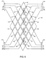
- Fig. 4 is an alternative embodiment of an optical add/drop switch 186 in accordance with the invention.
- the switch 186 includes four input ports 110-116, four output ports 118-124, four drop ports 126-132 and four add ports 134-140.
- the input ports are aligned with the output ports, rather than with the drop ports. It follows that the add ports are on the opposite side of the substrate 142 from the drop ports.
- the fourth switching arrangement 194 is in a transmissive state, the signals introduced at the fourth input port 116 will exit via the fourth output port 124. Signals that are introduced via the fourth add port 140 will enter the trench 210 and will be lost. By switching the two trenches 208 and 210 into their reflective states, the optical signals introduced via the input port 116 will exit via the drop port 132, while signals introduced via the fourth add port 140 will exit via the output port 124.
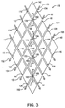
- the add/drop switch 100 of Fig. 3 is shown as being used in a wavelength-division multiplexed (WDM) arrangement.
- WDM wavelength-division multiplexed
- many data signals may be transmitted on a single optical fiber by using a different optical carrier wavelength for each signal.
- Wavelength demultiplexers 214 and 216 are used for feeding the input ports 110-116 and the add ports 134-140, respectively.
- the input 218 to the wavelength demultiplexer 214 may contain four optical signals having different carrier wavelengths, while the four outputs of the demultiplexer 214 will be dedicated to the different signals.
- the optical signal to the input 220 of the demultiplexer 216 will be divided into separate wavelength-based signals for introduction at the add ports 134-140.
- Two multiplexers 222 and 224 receive the separate signals from the output ports 118-124 and the drop ports 126-132, respectively. The separate signals are combined by the multiplexers for output via a single optical fiber 226 and 228.
- WDM has allowed telecommunications networks to greatly increase the transmission capabilities of optical fiber networks without installing new fiber.
- WDM in current networks is used for point-to-point transmission links, with optical transmitters at one node and optical receivers at the next node.
- only some of the traffic that arrives at a particular node has that node as its final destination.
- the remainder of the traffic is bound for downstream nodes. If local destination traffic can be concentrated or "groomed" into a relatively few number of incoming wavelength signals, the nodes with optical switching such as shown in Fig. 6 allow the express traffic to pass directly through the node, bypassing the local receivers and transmitters.
- Other applications of the invention are also contemplated.
Landscapes
- Physics & Mathematics (AREA)
- General Physics & Mathematics (AREA)
- Optics & Photonics (AREA)
- Mechanical Light Control Or Optical Switches (AREA)
- Use Of Switch Circuits For Exchanges And Methods Of Control Of Multiplex Exchanges (AREA)
- Optical Communication System (AREA)
Abstract
Description
Claims (10)
- An optical switch comprising:an array of side-by-side first optical paths (144, 146, 148 and 150);an array of side-by-side second optical paths (152, 154, 156 and 158), said first optical paths passing through said second optical paths at intersections;first ports (110, 112, 114 and 116) and second ports (126, 128, 130 and 132) at opposite sides of at least some of said first optical paths for propagating optical signals to and from said first optical paths;third ports (134, 136, 138 and 140) and fourth ports (118, 120, 122 and 124) at opposite sides of at least some of said second optical paths for propagating light to and from said second optical paths; anda plurality of two-state switching arrangements (102, 104, 106 and 108; and 188, 190, 192 and 194) located at selected said intersections such that each said first optical path includes and is uniquely associated with a single one of said two-state switching arrangements, each said two-state switching arrangement having a transmissive state in which said first and second ports of said uniquely associated first optical path are coupled, each said two-state switching arrangement having a reflective state in which said first port of said uniquely associated first optical path is coupled to a particular said fourth port of a specific second optical path.
- The optical switch of claim 1 wherein each said two-state switching arrangement (102, 104, 106 and 108) is an optical switching unit having a trench (168, 170, 172 and 174), said transmissive and reflective states of each said optical switching unit being dependent upon a presence of a selected fluid in said intersection at which said optical switching unit is located.
- The optical switch of claim 2 wherein there is a one-to-one correspondence between said optical switching units (102, 104, 106 and 108) and said first optical paths (144, 146, 148 and 150) and wherein:said first ports (110, 112, 114 and 116) are input ports;said second ports (126, 128, 130 and 132) are drop ports;said third ports (134, 136, 138 and 140) are add ports; andsaid fourth ports (118, 120, 122 and 124) are output ports.
- The optical switch of claim 3 wherein said two-state switching arrangements (102, 104, 106 and 108) are located at specific said intersections to provide an add-drop switch (100) in which each said add port (134, 136, 138 and 140) is uniquely associated with a different output port (118, 120, 122 and 124).
- The optical switch of claim 2, 3 or 4, wherein the number of first optical paths (144, 146, 148 and 150) is equal to the number of second optical paths (152, 154, 156 and 158).
- The optical switch of claim 1, wherein each said two-state switching arrangement (188, 190, 192 and 194) is comprised of a first trench (196, 200, 204 and 208) and a second trench (198, 202, 206 and 210), each said trench containing fluid responsive to manipulation such that by selectively manipulation of said fluid in said trench each said trench is capable of switching between a reflective state and a transmissive state, each said first trench and said second trench being operatively associated such that said first trench and said second trench are simultaneously in one of a reflective and a transmissive state.
- The optical switch of claim 6, wherein there is a one-to-one correspondence between said two-state switching arrangements (188, 190, 192 and 194) and said first optical paths and wherein:said first ports (110; 112, 114 and 116) are input ports;said second ports (118, 120, 122 and 124) are output ports;said third ports (134, 136, 138 and 140) are add ports; andsaid fourth ports (126, 128, 130 and 132) are drop ports.
- The optical switch of claim 6 or 7, wherein each said first trench (196, 200, 204 and 208) along a particular first optical path is located at said intersection of said particular first optical path with a corresponding one of said second optical paths.
- The optical switch of claim 8, wherein each said second trench (198, 202, 206 and 210) along a particular first optical path is located along said first optical path at said intersection that is adjacent to said intersection at which said first trench (196, 200, 204 and 208) of said two-state switching arrangements (188, 190, 192 and 194) is located.
- The optical switch of claim 9, wherein the number of first optical paths is equal to the number of second optical paths.
Applications Claiming Priority (2)
| Application Number | Priority Date | Filing Date | Title |
|---|---|---|---|
| US09/591,443 US6768830B1 (en) | 2000-06-09 | 2000-06-09 | Optical add/drop switch utilizing a minimal number of switching crosspoints |
| US591443 | 2000-06-09 |
Publications (2)
| Publication Number | Publication Date |
|---|---|
| EP1162484A2 true EP1162484A2 (en) | 2001-12-12 |
| EP1162484A3 EP1162484A3 (en) | 2004-07-14 |
Family
ID=24366507
Family Applications (1)
| Application Number | Title | Priority Date | Filing Date |
|---|---|---|---|
| EP01106914A Withdrawn EP1162484A3 (en) | 2000-06-09 | 2001-03-20 | Optical add/drop switch utilizing a minimal number of switching crosspoints |
Country Status (3)
| Country | Link |
|---|---|
| US (1) | US6768830B1 (en) |
| EP (1) | EP1162484A3 (en) |
| JP (1) | JP4819246B2 (en) |
Cited By (4)
| Publication number | Priority date | Publication date | Assignee | Title |
|---|---|---|---|---|
| EP1324084A3 (en) * | 2001-12-21 | 2004-10-13 | Agilent Technologies Inc. (a Delaware Corporation) | Method and apparatus for reducing optical insertion loss in integrated waveguide switches |
| US11256042B2 (en) * | 2018-04-03 | 2022-02-22 | Corning Research & Development Corporation | Waveguide substrates and waveguide substrate assemblies having waveguide routing schemes and methods for fabricating the same |
| US11372169B2 (en) | 2018-04-03 | 2022-06-28 | Corning Research & Development Corporation | Waveguide substrates and waveguide substrate connector assemblies having waveguides and alignment features and methods of fabricating the same |
| US11609395B2 (en) | 2021-01-11 | 2023-03-21 | Corning Research & Development Corporation | Waveguide substrates and assemblies including the same |
Families Citing this family (6)
| Publication number | Priority date | Publication date | Assignee | Title |
|---|---|---|---|---|
| WO2016064402A1 (en) | 2014-10-23 | 2016-04-28 | Hewlett Packard Enterprise Development Lp | Optical fiber interface for optical device package |
| WO2016064399A1 (en) * | 2014-10-23 | 2016-04-28 | Hewlett Packard Enterprise Development Lp | Optical port-shuffling module |
| US10534148B2 (en) | 2014-10-24 | 2020-01-14 | Hewlett Packard Enterprise Development Lp | Optical interconnect device |
| US10261256B2 (en) | 2015-01-28 | 2019-04-16 | Hewlett Packard Enterprise Development Lp | Laser-written optical routing systems and method |
| US10247969B1 (en) * | 2018-06-21 | 2019-04-02 | PsiQuantum Corp. | Photon sources with multiple cavities for generation of individual photons |
| US11199665B2 (en) * | 2020-01-28 | 2021-12-14 | Hewlett Packard Enterprise Development Lp | Optical device for redirecting optical signals |
Family Cites Families (11)
| Publication number | Priority date | Publication date | Assignee | Title |
|---|---|---|---|---|
| JP2539681B2 (en) * | 1989-03-17 | 1996-10-02 | アンリツ株式会社 | Optical path switching device |
| US4932745A (en) * | 1989-07-25 | 1990-06-12 | At&T Bell Laboratories | Radiation switching arrangement with moving deflecting element |
| US4988157A (en) | 1990-03-08 | 1991-01-29 | Bell Communications Research, Inc. | Optical switch using bubbles |
| JP3068415B2 (en) * | 1994-08-19 | 2000-07-24 | 日本電信電話株式会社 | Surface tension thermal control type waveguide optical switch and matrix type optical switch |
| US5699462A (en) | 1996-06-14 | 1997-12-16 | Hewlett-Packard Company | Total internal reflection optical switches employing thermal activation |
| JPH11202373A (en) * | 1998-01-13 | 1999-07-30 | Nippon Telegr & Teleph Corp <Ntt> | Light switch |
| US5960131A (en) | 1998-02-04 | 1999-09-28 | Hewlett-Packard Company | Switching element having an expanding waveguide core |
| US6055344A (en) | 1998-02-18 | 2000-04-25 | Hewlett-Packard Company | Fabrication of a total internal reflection optical switch with vertical fluid fill-holes |
| JP3566086B2 (en) * | 1998-07-08 | 2004-09-15 | 日本電信電話株式会社 | Optical switch array and optical add / drop multiplexer using the same |
| US6208778B1 (en) * | 1998-11-20 | 2001-03-27 | Agilent Technologies, Inc. | Non-perpendicular optical paths for a crosstalk-inhibiting switching arrangement |
| US6396972B1 (en) * | 2000-02-09 | 2002-05-28 | Agilent Technologies, Inc. | Thermally actuated optical add/drop switch |
-
2000
- 2000-06-09 US US09/591,443 patent/US6768830B1/en not_active Expired - Fee Related
-
2001
- 2001-03-20 EP EP01106914A patent/EP1162484A3/en not_active Withdrawn
- 2001-05-29 JP JP2001160732A patent/JP4819246B2/en not_active Expired - Fee Related
Cited By (4)
| Publication number | Priority date | Publication date | Assignee | Title |
|---|---|---|---|---|
| EP1324084A3 (en) * | 2001-12-21 | 2004-10-13 | Agilent Technologies Inc. (a Delaware Corporation) | Method and apparatus for reducing optical insertion loss in integrated waveguide switches |
| US11256042B2 (en) * | 2018-04-03 | 2022-02-22 | Corning Research & Development Corporation | Waveguide substrates and waveguide substrate assemblies having waveguide routing schemes and methods for fabricating the same |
| US11372169B2 (en) | 2018-04-03 | 2022-06-28 | Corning Research & Development Corporation | Waveguide substrates and waveguide substrate connector assemblies having waveguides and alignment features and methods of fabricating the same |
| US11609395B2 (en) | 2021-01-11 | 2023-03-21 | Corning Research & Development Corporation | Waveguide substrates and assemblies including the same |
Also Published As
| Publication number | Publication date |
|---|---|
| JP4819246B2 (en) | 2011-11-24 |
| US6768830B1 (en) | 2004-07-27 |
| JP2002058050A (en) | 2002-02-22 |
| EP1162484A3 (en) | 2004-07-14 |
Similar Documents
| Publication | Publication Date | Title |
|---|---|---|
| EP1045277A1 (en) | Fault tolerant optical switch matrix | |
| KR20130112912A (en) | Core-selective optical switches | |
| JPH11289562A (en) | Add wavelength selectivity-drop device | |
| JP5913139B2 (en) | Waveguide type optical switch | |
| US6768830B1 (en) | Optical add/drop switch utilizing a minimal number of switching crosspoints | |
| US6396972B1 (en) | Thermally actuated optical add/drop switch | |
| US6956987B2 (en) | Planar lightwave wavelength blocker devices using micromachines | |
| US6320995B1 (en) | Loss equalization by means of port interconnectivity in a multistage optical switch | |
| US6819821B2 (en) | Optical switch with a geometry based on perpendicularly-oriented planar lightwave circuit switches | |
| CN114924357A (en) | A Wavelength Division Multiplexing Optical Delay Line Based on Cascaded Mach-Zehnder Interferometer Structure | |
| CN120826633A (en) | Polarization-diversity integrated photonic switch with multilayer waveguides | |
| JP2001156716A (en) | Add / drop optical multiplexer and method for adding channels | |
| CA2386352A1 (en) | Nxn optical matrix switch using modified cross-connect of 1xn switches | |
| JP6420715B2 (en) | Optical signal processor | |
| JP4766767B2 (en) | Low loss reconfigurable optical add / drop multiplexer switch | |
| US6891989B2 (en) | Optical switch systems using waveguide grating-based wavelength selective switch modules | |
| US6879754B2 (en) | Drop-before-add optical switching and routing system employing grating-based wavelength selective switches | |
| US6724952B2 (en) | Wavelength selective cross-connect (WSC) | |
| CN114236696A (en) | 1×N wavelength selective switch | |
| Doerr et al. | Silica-waveguide 1× 9 wavelength-selective cross connect | |
| JP3566086B2 (en) | Optical switch array and optical add / drop multiplexer using the same | |
| EP1371260B1 (en) | Polarization independent non-bloking all-optical switching device | |
| CN1751254A (en) | Optical switch systems using waveguide grating-based wavelength selective switch modules | |
| Fouquet | Progress in optical cross-connects for circuit-switched applications | |
| EP0916982A2 (en) | Optical switch |
Legal Events
| Date | Code | Title | Description |
|---|---|---|---|
| PUAI | Public reference made under article 153(3) epc to a published international application that has entered the european phase |
Free format text: ORIGINAL CODE: 0009012 |
|
| AK | Designated contracting states |
Kind code of ref document: A2 Designated state(s): AT BE CH CY DE DK ES FI FR GB GR IE IT LI LU MC NL PT SE TR |
|
| AX | Request for extension of the european patent |
Free format text: AL;LT;LV;MK;RO;SI |
|
| PUAL | Search report despatched |
Free format text: ORIGINAL CODE: 0009013 |
|
| AK | Designated contracting states |
Kind code of ref document: A3 Designated state(s): AT BE CH CY DE DK ES FI FR GB GR IE IT LI LU MC NL PT SE TR |
|
| AX | Request for extension of the european patent |
Extension state: AL LT LV MK RO SI |
|
| RIC1 | Information provided on ipc code assigned before grant |
Ipc: 7G 02B 6/35 B Ipc: 7G 02B 6/293 A |
|
| 17P | Request for examination filed |
Effective date: 20041216 |
|
| 17Q | First examination report despatched |
Effective date: 20040209 |
|
| AKX | Designation fees paid |
Designated state(s): DE FR GB |
|
| STAA | Information on the status of an ep patent application or granted ep patent |
Free format text: STATUS: THE APPLICATION IS DEEMED TO BE WITHDRAWN |
|
| 18D | Application deemed to be withdrawn |
Effective date: 20050621 |