EP1162483A2 - Optimization of optical waveguide positions and angles for efficient coupling of reflected waves - Google Patents
Optimization of optical waveguide positions and angles for efficient coupling of reflected waves Download PDFInfo
- Publication number
- EP1162483A2 EP1162483A2 EP01106813A EP01106813A EP1162483A2 EP 1162483 A2 EP1162483 A2 EP 1162483A2 EP 01106813 A EP01106813 A EP 01106813A EP 01106813 A EP01106813 A EP 01106813A EP 1162483 A2 EP1162483 A2 EP 1162483A2
- Authority
- EP
- European Patent Office
- Prior art keywords
- light
- interface
- waveguides
- waveguide
- optical
- Prior art date
- Legal status (The legal status is an assumption and is not a legal conclusion. Google has not performed a legal analysis and makes no representation as to the accuracy of the status listed.)
- Withdrawn
Links
- 230000003287 optical effect Effects 0.000 title claims abstract description 46
- 230000008878 coupling Effects 0.000 title claims abstract description 32
- 238000010168 coupling process Methods 0.000 title claims abstract description 32
- 238000005859 coupling reaction Methods 0.000 title claims abstract description 32
- 238000005457 optimization Methods 0.000 title 1
- 230000010287 polarization Effects 0.000 claims abstract description 56
- 230000000694 effects Effects 0.000 claims abstract description 10
- 239000012530 fluid Substances 0.000 claims description 20
- 238000000034 method Methods 0.000 claims description 8
- 230000001902 propagating effect Effects 0.000 claims description 5
- 230000001419 dependent effect Effects 0.000 abstract description 15
- 239000011162 core material Substances 0.000 description 12
- 238000005253 cladding Methods 0.000 description 9
- 239000000463 material Substances 0.000 description 7
- VYPSYNLAJGMNEJ-UHFFFAOYSA-N Silicium dioxide Chemical compound O=[Si]=O VYPSYNLAJGMNEJ-UHFFFAOYSA-N 0.000 description 6
- KFZMGEQAYNKOFK-UHFFFAOYSA-N Isopropanol Chemical compound CC(C)O KFZMGEQAYNKOFK-UHFFFAOYSA-N 0.000 description 3
- 238000005530 etching Methods 0.000 description 3
- 230000008569 process Effects 0.000 description 3
- 235000012239 silicon dioxide Nutrition 0.000 description 3
- 239000000377 silicon dioxide Substances 0.000 description 3
- 238000012546 transfer Methods 0.000 description 3
- 238000013459 approach Methods 0.000 description 2
- 238000004891 communication Methods 0.000 description 2
- 238000006073 displacement reaction Methods 0.000 description 2
- 238000012545 processing Methods 0.000 description 2
- 239000000758 substrate Substances 0.000 description 2
- 230000009471 action Effects 0.000 description 1
- 230000004913 activation Effects 0.000 description 1
- 230000002457 bidirectional effect Effects 0.000 description 1
- 230000005540 biological transmission Effects 0.000 description 1
- 230000015572 biosynthetic process Effects 0.000 description 1
- 238000006243 chemical reaction Methods 0.000 description 1
- 238000000059 patterning Methods 0.000 description 1
Images



Classifications
-
- G—PHYSICS
- G02—OPTICS
- G02B—OPTICAL ELEMENTS, SYSTEMS OR APPARATUS
- G02B6/00—Light guides; Structural details of arrangements comprising light guides and other optical elements, e.g. couplings
- G02B6/24—Coupling light guides
- G02B6/26—Optical coupling means
- G02B6/35—Optical coupling means having switching means
- G02B6/3596—With planar waveguide arrangement, i.e. in a substrate, regardless if actuating mechanism is outside the substrate
-
- G—PHYSICS
- G02—OPTICS
- G02B—OPTICAL ELEMENTS, SYSTEMS OR APPARATUS
- G02B26/00—Optical devices or arrangements for the control of light using movable or deformable optical elements
- G02B26/004—Optical devices or arrangements for the control of light using movable or deformable optical elements based on a displacement or a deformation of a fluid
-
- G—PHYSICS
- G02—OPTICS
- G02B—OPTICAL ELEMENTS, SYSTEMS OR APPARATUS
- G02B6/00—Light guides; Structural details of arrangements comprising light guides and other optical elements, e.g. couplings
- G02B6/24—Coupling light guides
- G02B6/26—Optical coupling means
- G02B6/35—Optical coupling means having switching means
- G02B6/3538—Optical coupling means having switching means based on displacement or deformation of a liquid
-
- G—PHYSICS
- G02—OPTICS
- G02B—OPTICAL ELEMENTS, SYSTEMS OR APPARATUS
- G02B6/00—Light guides; Structural details of arrangements comprising light guides and other optical elements, e.g. couplings
- G02B6/24—Coupling light guides
- G02B6/26—Optical coupling means
- G02B6/35—Optical coupling means having switching means
- G02B6/354—Switching arrangements, i.e. number of input/output ports and interconnection types
- G02B6/3544—2D constellations, i.e. with switching elements and switched beams located in a plane
- G02B6/3546—NxM switch, i.e. a regular array of switches elements of matrix type constellation
-
- G—PHYSICS
- G02—OPTICS
- G02B—OPTICAL ELEMENTS, SYSTEMS OR APPARATUS
- G02B6/00—Light guides; Structural details of arrangements comprising light guides and other optical elements, e.g. couplings
- G02B6/24—Coupling light guides
- G02B6/26—Optical coupling means
- G02B6/35—Optical coupling means having switching means
- G02B6/3564—Mechanical details of the actuation mechanism associated with the moving element or mounting mechanism details
- G02B6/3568—Mechanical details of the actuation mechanism associated with the moving element or mounting mechanism details characterised by the actuating force
- G02B6/3576—Temperature or heat actuation
Definitions
- the invention relates generally to efficiently coupling optical waveguides and more particularly to determining the positions and angles of waveguides relative to a plane of total internal reflection.
- the localized manipulation may be a steady-state signal transfer arrangement between two waveguides or may be a switching arrangement in which an optical signal along one waveguide can be transferred to any one of a number of output waveguides.
- TIR total internal reflection
- the switching unit includes planar waveguides that are formed by layers on a substrate.
- the waveguide layers include a lower cladding layer 14, an optical core 16, and an upper cladding layer, not shown.
- the optical core may be primarily silicon dioxide, but with doping materials that achieve a desired index of refraction.
- the cladding layers are formed of a material having a refractive index that is significantly different than that of the core material, so that the optical signals are guided along the core.
- the effective phase index of the waveguide is determined by the refractive indices of the core material and the material of the cladding layers, as is well known in the art.
- the layer of core material is patterned into waveguide segments that define a first input waveguide 20 and a first output waveguide 26 of a first optical path.
- the patterning also defines a second input waveguide 24 and a second output waveguide 22 of a second linear path.
- the upper cladding layer is then deposited over the patterned core material.
- a gap is formed by etching a trench 28 through the core material, the upper cladding layer, and at least a portion of the lower cladding layer 14.
- the first input waveguide 20 and the second output waveguide 22 have axes that intersect a sidewall of the trench 28 at an angle of incidence that results in TIR diverting light from the input waveguide 20 to the output waveguide 22 when the junction 30 of the waveguides is filled with vapor or gas.
- the junction 30 is filled with a fluid that has an index of refraction substantially matching that of the effective phase index of the waveguides, light from the input waveguide 20 will travel through the index-matching fluid to the linearly aligned first output waveguide 26.
- the patent to Fouquet et al. describes a number of alternative embodiments to switching the optical switching unit 10 between a transmitting state and reflecting state.
- the two input waveguides 20 and 24 are optically coupled to their linearly aligned output waveguides 26 and 22, respectively.
- the first input waveguide 20 is optically coupled to the second output waveguide 22, but the second input waveguide 24 is not in communication with either of the output waveguides 22 and 26.
- One approach to switching between the two states is illustrated in Fig. 1.
- the switching unit 10 includes a microheater 38 that controls formation of a bubble within the fluid-containing trench.
- the heater When the heater is brought to a temperature that is sufficiently high to form a bubble in the index-matching fluid, the bubble is positioned at the junction 30 of the four waveguides. Consequently, light propagating along the waveguide 20 encounters a refractive index mismatch upon reaching the sidewall of the trench 28, causing TIR, so that the waveguides 20 and 22 are optically coupled. However, when the heater 38 is deactivated, the index-matching fluid will again reside within the junction between the four waveguides.
- Fig. 1 The principles described with reference to Fig. 1 also apply to a steady-state reflecting arrangement. That is, if the index-matching fluid is removed from the trench 28, the waveguides 20 and 22 will be continuously coupled by TIR at the wall of the trench. In this steady-state embodiment, the waveguides 24 and 26 would not be included.
- TIR transverse electric
- TM transverse magnetic
- Optical efficiency in the coupling of two waveguides that intersect an interface between high and low refractive index regions is enhanced by determining compensation for the Goos-Hänchen effect along the interface.
- the lateral shift of reflected light along the interface is predicted in order to determine a distance at which the axes of the two waveguides should be spaced apart along the interface.
- the incidence angles of the two waveguides are selected so as to equalize the lateral shifts for the polarizations, since light collection by the second waveguide can be increased by selection of the proper angle, even if the spacing between the two waveguide axes remains fixed.
- both the distance between the axes and the incidence angles are selected to provide compensation for the Goos-Hänchen effect.
- TIR occurs when a ray of light impinges the interface between the high and low refractive index regions from the high index side.
- the Goos-Hänchen effect causes the reflected light to emerge from the interface a short distance away from the point at which the incident light intersects the interface.
- the optimal positioning is polarization dependent. That is, the lateral shift (z TM ) of light having a TM polarization is different than the lateral shift (z TE ) of light having a TE polarization. Reflection can be optimized for either the TM polarization or the TE polarization.
- the distance between the axes of the waveguides along the interface can be selected to equalize the loss for the two polarizations.
- a zero-polarization dependent loss (PDL) for the reflection can be approached. This provides an acceptable overall low loss arrangement.
- the z TM and z TE values can be converted using known trigonometric relations to a beam displacement from the position that the beam would be obtained if a geometrical reflection were to have occurred.
- the conversion can be used to determine the signal attenuation that would occur if two waveguides were at geometrical reflection positions.
- the loss can be eliminated by arranging the two waveguides to intersect the plane of total internal reflection such that the axes of the waveguides are spaced apart by the desired distance.
- This step of arranging the waveguides may be performed by fabricating the waveguides to end at a preselected plane that defines the interface.
- the waveguides can be fabricated to have intersecting axes, but then truncating along the plane that provides the desired spacing between the two axes.
- the spacing may be selected based solely upon the determination of z TM , or solely upon the determination of z TE , or upon the average between z TM and z TE .
- the incidence angles for a particular application of folding a beam path that includes propagation along two waveguides can be selected to minimize polarization dependent loss. Since the lateral shifts of Eq. 1 and Eq. 2 are dependent upon the incidence angle ( ⁇ ), the selection of the equal angles of incidence of the two waveguides relative to the normal of the interface is a function of the refractive index (n f ) of the waveguides (i.e., the effective phase index of the waveguides) and the refractive index (n s ) of the region on a side of the interface opposite to the waveguides. Solving Eq. 1 and Eq.
- the incidence angle can be optimized for one polarization or the other, but Eq. 4 is preferably used to determine the condition in which the polarization dependent loss is theoretically zero.
- n s is the refractive index of air and the waveguides are formed of materials that provide an effective phase index (n f ) in the range of 1.30 to 1.60
- the range of incidence angles determined using Eq. 4 will be 48° to 60°.
- total internal reflection occurs when input light 40 that is propagating along an optical path having a high refractive index impinges upon an interface 42 that is the boundary to a region having a low refractive index.
- the low refractive index region may be an air-filled region.
- the input light 40 randomly varies between having a transverse electric polarization and a transverse magnetic polarization.
- the two polarizations are represented by symbols 44 and 46 in Fig. 2.
- the reflected light emerges from the interface 42 at a short distance from the point at which the input light 40 impinges the interface. The distance will depend upon the current polarization of the input light.
- the output light 48 having a TM polarization is shown as emerging at a shorter distance (z TM ) from the point of impingement than the distance (z TE ) from which output light 50 having a TE polarization emerges.
- a designer of an optical coupling arrangement may elect to optimize coupling of light having a particular polarization by positioning an output waveguide at either the location of output beam 48 or the location of output beam 50.
- the distance between the axes of an input waveguide and an output waveguide would be either z TM or z TE .
- the designer may attempt to provide a zero polarization dependent loss by positioning the output waveguide at the distance shown as z AVE , which is the average of distances z TM and z TE .
- Forming a highly efficient optical coupling arrangement also requires consideration of the incidence angles of the waveguides.
- the incidence angle is one factor in determining the lateral shift from the beam axis of input light 40 to the beam axes of the two polarization-dependent output lights 48 and 50.
- the same shift of the two polarizations can be achieved, so that an output beam 52 has a theoretical polarization dependent loss of zero.
- the angle at which this occurs depends on the refractive indices of the waveguides and the region on the opposite side of the interface 42.
- a steady-state optical coupling arrangement 54 is shown as including an input waveguide 56 and an output waveguide 58 that intersect a trench 60.
- the waveguides are formed on a substrate 62.
- the structure of the waveguides may be identical to the structure described with reference to Fig. 1. That is, the waveguides may be formed of a patterned layer of silicon dioxide that is doped to provide a waveguide core having a desired refractive index, with cladding layers being formed around the core to trap propagating light within the core material.
- doped silicon dioxide to form waveguides is not critical to the invention.
- the trench 60 may be formed by etching the core material and the cladding layers to provide an air-filled region, so that the refractive index is significantly lower than the effective phase index of the waveguides.
- other techniques for achieving an interface between higher and lower refractive indices may be employed.
- the input waveguide 56 has an axis 64 that intersects the wall of the trench 60 at a point that is spaced apart from the point of intersection of an axis 66 of the output waveguide 58.
- Total internal reflection provides a folded beam path as light from the input waveguide 56 impinges upon the sidewall of the trench 60.
- the angles of incidence are equal, but are shown separately in Fig. 3 as being the angle ⁇ 1 between the input waveguide axis 64 and the normal of the sidewall of the trench 60 and the angle ⁇ 2 between the output waveguide axis 66 and the normal to the sidewall of the trench.
- the distance between the points at which the axes 64 and 66 intersect the sidewall of the trench 60 may be varied.
- the waveguides are formed but the position of the trench 60 is negotiable, so that any one of the three distances z TM , z TE or z AVE of Fig. 2 may be established by precisely etching the trench 60 in the appropriate location.
- the distance between the intersection points of the waveguide axes upon the trench is fixed, but the incidence angle is negotiable.
- the geometry of the waveguides and the interface is selected to provide efficient coupling from the input waveguide 56 to the output waveguide 58.
- waveguides 56 and 58 will be described as being input and output waveguides, bidirectional coupling is available in the geometry shown in Fig. 3. That is, a beam which is introduced to the waveguide 58 from an external source will reflect from the sidewall of the trench 60 to the waveguide 56 at an efficiency that equals the efficiency of propagation in the opposite direction.
- this equation may be used.
- the result is that there will be a high polarization dependent loss, since the optical coupling arrangement will be polarization preferential.
- the polarization selectivity may be desired in some applications.
- z TE 2(N 2 -n 2 s ) -1/2 tan ( ⁇ )/k
- the goal is to minimize the polarization dependent loss for the reflection from the input waveguide 56 to the output waveguide 58.
- this may be achieved by separating the two waveguide axes 64 and 66 by a distance that is the average of z TM and z TE .
- the transmission into the receiving waveguide 58 has a transfer coefficient that is approximately Gaussian with respect to the offset between the center of the beam of light and the axis 66 of the receiving waveguide. Therefore, the signal loss is predictable and within acceptable tolerances.
- the angle of incidence is selected in order to achieve an optically efficient coupling arrangement between the input waveguide 56 and the output waveguide 58.
- the two polarizations will experience the same lateral shift.
- the incidence angle can be readily calculated.
- n s is the refractive index of air and the waveguides are formed of materials that provide a refractive index (n f ) in the range of 1.30 to 1.60
- the range of incidence angles determined using Eq. 3 is indicated in Table 1. It should be noted that the refractive index referred to within Table 1 is the effective phase index of the waveguide, which means that a typical waveguide would require an incidence angle of approximately 53°.
- Fig. 4 illustrates a switching arrangement 68 in accordance with the invention.
- the switching arrangement includes two input waveguides 70 and 72 and two output waveguides 74 and 76.
- the switching arrangement is shown in a reflecting state in Fig. 4.
- a microheater 78 is activated to heat fluid 80 within a trench 82.
- the fluid has a refractive index that substantially matches the effective phase index of the waveguides.
- One acceptable fluid is isopropyl alcohol.
- the activation of the microheater 78 causes a gas bubble to be formed at the junction of the four waveguides, thereby creating a total internal reflection interface at the sidewall of the trench 82.
- the input waveguide 70 is optically coupled to the output waveguide 74.
- the axis of the waveguide 76 is sufficiently spaced apart from the axis of the input waveguide 72 to prevent optical coupling between the input and output waveguide 72 and 76.
- the fluid 80 within the trench 82 will occupy the portion of the trench 82 at the junction of the four waveguides 70, 72, 74 and 76. Because the fluid has a refractive index which substantially matches the effective phase index of the waveguides, the switching arrangement 68 will be in a transmitting state. Signals introduced via the input waveguide 70 will propagate through the index-matching fluid to the output waveguide 76. Similarly, optical signals introduced via the input waveguide 72 will propagate through the fluid to the output waveguide 74.
- Other approaches to manipulating fluid relative to the junction of the four waveguides may be substituted. For example, the techniques used in inkjet printheads may be used to fire the index-matching fluid from the junction of the waveguides, with capillary action being used to replenish the fluid.
- one embodiment for providing an efficient optical coupling of waveguides using a total internal reflection (TIR) interface includes a step 84 of determining a lateral shift for light having a TM polarization. This step may be carried out using Eq. 1.
- step 86 the lateral shift of light having a TE polarization is determined. The calculation may be based on Eq. 2.
- only one of the steps 84 and 86 is utilized, since there may be applications in which coupling of only one of the TM polarized light or the TE polarized light is preferred.
- step 88 the calculated relationship between the waveguides and a TIR interface is established.
- the waveguides are patterned relative to a fixed TIR interface.
- the waveguides are fabricated to have intersecting axes, but waveguide material is then etched to form the TIR interface at the desired location, with the axes being spaced apart at the TIR interface as described with reference to Figs. 3 and 4.
- step 90 of Fig. 6 includes determining the incidence angle that provides a generally equal lateral shift of beams having TM and TE polarizations. Eq. 4 may be used in implementing step 90. The determination of the incidence angle is then used at step 92 to establish a calculated relationship between each of the waveguides and a TIR interface. As a result, a polarization dependent loss of approximately zero is achieved simultaneously with a reflection loss of zero.
Landscapes
- Physics & Mathematics (AREA)
- General Physics & Mathematics (AREA)
- Optics & Photonics (AREA)
- Optical Integrated Circuits (AREA)
- Mechanical Light Control Or Optical Switches (AREA)
Abstract
Description
- The invention relates generally to efficiently coupling optical waveguides and more particularly to determining the positions and angles of waveguides relative to a plane of total internal reflection.
- Increasingly, signal transfers within a telecommunications or data communications environment are being carried out using optical networks. Information can be exchanged in the form of modulations of laser-produced light. The equipment for efficiently generating optical signals and the cables for transmitting the optical signals over extended distances are readily available. However, there are still some concerns with regard to enabling localized manipulation of signals without a significant sacrifice of signal strength. The localized manipulation may be a steady-state signal transfer arrangement between two waveguides or may be a switching arrangement in which an optical signal along one waveguide can be transferred to any one of a number of output waveguides.
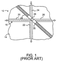
- One technique for redirecting an optical signal from one waveguide to another waveguide is to use a mirror. The mirror may be stationary or may be used in a switching arrangement by connecting the mirror to a micromachine device. An alternative to using the mirror is to provide a plane of total internal reflection (TIR). As is known in the art, TIR occurs when a ray of light travels toward an interface between a region having a high refractive index and a region of low refractive index, with the ray of light approaching from the high index side of the interface. A switching arrangement that utilizes the phenomenon of TIR is described in U.S. Pat. No. 5,699,462 to Fouquet et al., which is assigned to the assignee of the present invention. An isolated switching unit 10 is shown in Fig. 1. The switching unit includes planar waveguides that are formed by layers on a substrate. The waveguide layers include a lower cladding layer 14, an optical core 16, and an upper cladding layer, not shown. The optical core may be primarily silicon dioxide, but with doping materials that achieve a desired index of refraction. The cladding layers are formed of a material having a refractive index that is significantly different than that of the core material, so that the optical signals are guided along the core. The effective phase index of the waveguide is determined by the refractive indices of the core material and the material of the cladding layers, as is well known in the art. The layer of core material is patterned into waveguide segments that define a first input waveguide 20 and a first output waveguide 26 of a first optical path. The patterning also defines a second input waveguide 24 and a second output waveguide 22 of a second linear path. The upper cladding layer is then deposited over the patterned core material. A gap is formed by etching a trench 28 through the core material, the upper cladding layer, and at least a portion of the lower cladding layer 14.
- The first input waveguide 20 and the second output waveguide 22 have axes that intersect a sidewall of the trench 28 at an angle of incidence that results in TIR diverting light from the input waveguide 20 to the output waveguide 22 when the junction 30 of the waveguides is filled with vapor or gas. However, when the junction 30 is filled with a fluid that has an index of refraction substantially matching that of the effective phase index of the waveguides, light from the input waveguide 20 will travel through the index-matching fluid to the linearly aligned first output waveguide 26.
- The patent to Fouquet et al. describes a number of alternative embodiments to switching the optical switching unit 10 between a transmitting state and reflecting state. In the transmitting state, the two input waveguides 20 and 24 are optically coupled to their linearly aligned output waveguides 26 and 22, respectively. In the reflecting state, the first input waveguide 20 is optically coupled to the second output waveguide 22, but the second input waveguide 24 is not in communication with either of the output waveguides 22 and 26. One approach to switching between the two states is illustrated in Fig. 1. The switching unit 10 includes a microheater 38 that controls formation of a bubble within the fluid-containing trench. When the heater is brought to a temperature that is sufficiently high to form a bubble in the index-matching fluid, the bubble is positioned at the junction 30 of the four waveguides. Consequently, light propagating along the waveguide 20 encounters a refractive index mismatch upon reaching the sidewall of the trench 28, causing TIR, so that the waveguides 20 and 22 are optically coupled. However, when the heater 38 is deactivated, the index-matching fluid will again reside within the junction between the four waveguides.
- The principles described with reference to Fig. 1 also apply to a steady-state reflecting arrangement. That is, if the index-matching fluid is removed from the trench 28, the waveguides 20 and 22 will be continuously coupled by TIR at the wall of the trench. In this steady-state embodiment, the waveguides 24 and 26 would not be included.
- While the phenomenon of TIR has been used successfully in the redirection of optical signals from one waveguide to another waveguide, further improvements are desired. Light that impinges an interface between a high refractive index region and a low refractive index region will vary between having a transverse electric (TE) polarization and having a transverse magnetic (TM) polarization. The light will react differently at the interface, depending upon its polarization. Consequently, there are polarization dependent losses (PDLs) due to imperfect coupling to the waveguide modes. Since light impinging the interface will randomly vary between polarizations, the variations in PDL are random.
- What is needed is an optical coupling arrangement of waveguides in which polarization dependent losses are neutralized or rendered predictable. What is also needed is a method of determining efficient layouts for positioning waveguides relative to a TIR interface.
- Optical efficiency in the coupling of two waveguides that intersect an interface between high and low refractive index regions is enhanced by determining compensation for the Goos-Hänchen effect along the interface. In one embodiment, the lateral shift of reflected light along the interface is predicted in order to determine a distance at which the axes of the two waveguides should be spaced apart along the interface. In another embodiment, the incidence angles of the two waveguides are selected so as to equalize the lateral shifts for the polarizations, since light collection by the second waveguide can be increased by selection of the proper angle, even if the spacing between the two waveguide axes remains fixed. In the preferred embodiment, both the distance between the axes and the incidence angles are selected to provide compensation for the Goos-Hänchen effect.
- As previously noted, TIR occurs when a ray of light impinges the interface between the high and low refractive index regions from the high index side. However, the Goos-Hänchen effect causes the reflected light to emerge from the interface a short distance away from the point at which the incident light intersects the interface. By tailoring the positions and/or the angles of waveguides to maximize the collection of the reflected light, the reliability of signal processing can be improved. The optimal positioning is polarization dependent. That is, the lateral shift (zTM) of light having a TM polarization is different than the lateral shift (zTE) of light having a TE polarization. Reflection can be optimized for either the TM polarization or the TE polarization. Alternatively, the distance between the axes of the waveguides along the interface can be selected to equalize the loss for the two polarizations. By selecting the distance to be one-half of the difference between the two optimal points of the two polarizations, a zero-polarization dependent loss (PDL) for the reflection can be approached. This provides an acceptable overall low loss arrangement.
- The lateral shift of light having the TM polarization may be calculated on the basis of the following equation:
- The incidence angles for a particular application of folding a beam path that includes propagation along two waveguides can be selected to minimize polarization dependent loss. Since the lateral shifts of Eq. 1 and Eq. 2 are dependent upon the incidence angle (), the selection of the equal angles of incidence of the two waveguides relative to the normal of the interface is a function of the refractive index (nf) of the waveguides (i.e., the effective phase index of the waveguides) and the refractive index (ns) of the region on a side of the interface opposite to the waveguides. Solving Eq. 1 and Eq. 2 for the condition that provides a substantially equal shift for the two polarizations provides the alternative equations:
-
- Fig. 1 is a top view of an optical switching unit that utilizes total internal reflection in accordance with the prior art.
- Fig. 2 is a representation of total internal reflection as a result of the Goos-Hänchen effect.
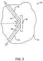
- Fig. 3 is a top view of a steady-state optical switching arrangement in accordance with the invention.
- Fig. 4 is a top view of a switching arrangement in accordance with the invention.
- Fig. 5 is a process flow of steps for implementing one embodiment of the invention.
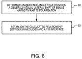
- Fig. 6 is a process flow of steps for implementing an alternative or additional embodiment of the invention.
-
- With reference to Fig. 2, total internal reflection occurs when input light 40 that is propagating along an optical path having a high refractive index impinges upon an interface 42 that is the boundary to a region having a low refractive index. For example, the low refractive index region may be an air-filled region. The input light 40 randomly varies between having a transverse electric polarization and a transverse magnetic polarization. The two polarizations are represented by symbols 44 and 46 in Fig. 2. As a result of the phenomenon known as the Goos-Hänchen effect, the reflected light emerges from the interface 42 at a short distance from the point at which the input light 40 impinges the interface. The distance will depend upon the current polarization of the input light. In Fig. 2, the output light 48 having a TM polarization is shown as emerging at a shorter distance (zTM) from the point of impingement than the distance (zTE) from which output light 50 having a TE polarization emerges.
- In view of the Goos-Hänchen effect, a designer of an optical coupling arrangement may elect to optimize coupling of light having a particular polarization by positioning an output waveguide at either the location of output beam 48 or the location of output beam 50. Thus, the distance between the axes of an input waveguide and an output waveguide would be either zTM or zTE. On the other hand, the designer may attempt to provide a zero polarization dependent loss by positioning the output waveguide at the distance shown as zAVE, which is the average of distances zTM and zTE.
- Forming a highly efficient optical coupling arrangement also requires consideration of the incidence angles of the waveguides. As will be explained more fully below, the incidence angle is one factor in determining the lateral shift from the beam axis of input light 40 to the beam axes of the two polarization-dependent output lights 48 and 50. By selecting the proper angles of the waveguides, the same shift of the two polarizations can be achieved, so that an output beam 52 has a theoretical polarization dependent loss of zero. The angle at which this occurs depends on the refractive indices of the waveguides and the region on the opposite side of the interface 42.
- Referring now to Fig. 3, a steady-state optical coupling arrangement 54 is shown as including an input waveguide 56 and an output waveguide 58 that intersect a trench 60. The waveguides are formed on a substrate 62. The structure of the waveguides may be identical to the structure described with reference to Fig. 1. That is, the waveguides may be formed of a patterned layer of silicon dioxide that is doped to provide a waveguide core having a desired refractive index, with cladding layers being formed around the core to trap propagating light within the core material. However, the use of doped silicon dioxide to form waveguides is not critical to the invention. The trench 60 may be formed by etching the core material and the cladding layers to provide an air-filled region, so that the refractive index is significantly lower than the effective phase index of the waveguides. However, other techniques for achieving an interface between higher and lower refractive indices may be employed.
- The input waveguide 56 has an axis 64 that intersects the wall of the trench 60 at a point that is spaced apart from the point of intersection of an axis 66 of the output waveguide 58. Total internal reflection provides a folded beam path as light from the input waveguide 56 impinges upon the sidewall of the trench 60. By tailoring the positions and/or the angles of the waveguides to maximize the collection of the reflected light, the reliability of signal processing can be enhanced. The angles of incidence are equal, but are shown separately in Fig. 3 as being the angle 1 between the input waveguide axis 64 and the normal of the sidewall of the trench 60 and the angle 2 between the output waveguide axis 66 and the normal to the sidewall of the trench. If the angles 1 and 2 are fixed, the distance between the points at which the axes 64 and 66 intersect the sidewall of the trench 60 may be varied. For example, there may be applications in which the waveguides are formed but the position of the trench 60 is negotiable, so that any one of the three distances zTM, zTE or zAVE of Fig. 2 may be established by precisely etching the trench 60 in the appropriate location. On the other hand, there may be applications in which the distance between the intersection points of the waveguide axes upon the trench is fixed, but the incidence angle is negotiable. Depending upon the application, the geometry of the waveguides and the interface is selected to provide efficient coupling from the input waveguide 56 to the output waveguide 58.
- While the waveguides 56 and 58 will be described as being input and output waveguides, bidirectional coupling is available in the geometry shown in Fig. 3. That is, a beam which is introduced to the waveguide 58 from an external source will reflect from the sidewall of the trench 60 to the waveguide 56 at an efficiency that equals the efficiency of propagation in the opposite direction.
- For a given incidence angle, the lateral shift of light having the TM polarization may be calculated on the basis of the following equation:
- In any applications in which selectivity of light having the TE polarization is desired, the following equation may be used:
- In a third application, the goal is to minimize the polarization dependent loss for the reflection from the input waveguide 56 to the output waveguide 58. For a given waveguide incidence angle, this may be achieved by separating the two waveguide axes 64 and 66 by a distance that is the average of zTM and zTE. As a result, the transmission into the receiving waveguide 58 has a transfer coefficient that is approximately Gaussian with respect to the offset between the center of the beam of light and the axis 66 of the receiving waveguide. Therefore, the signal loss is predictable and within acceptable tolerances.
- In another embodiment, the angle of incidence is selected in order to achieve an optically efficient coupling arrangement between the input waveguide 56 and the output waveguide 58. By selecting the proper incidence angle, the two polarizations will experience the same lateral shift. The condition that provides the same shift for the two polarizations is determined by the formula:
nf , degrees 1.30 59.59 1.32 58.66 1.34 57.77 1.36 56.92 1.38 56.10 1.40 55.30 1.42 54.53 1.44 53.78 1.46 53.06 1.48 52.36 1.50 51.68 1.52 51.02 1.54 50.38 1.56 49.76 1.58 49.15 1.60 48.56 - Fig. 4 illustrates a switching arrangement 68 in accordance with the invention. The switching arrangement includes two input waveguides 70 and 72 and two output waveguides 74 and 76. The switching arrangement is shown in a reflecting state in Fig. 4. In this state, a microheater 78 is activated to heat fluid 80 within a trench 82. The fluid has a refractive index that substantially matches the effective phase index of the waveguides. One acceptable fluid is isopropyl alcohol. The activation of the microheater 78 causes a gas bubble to be formed at the junction of the four waveguides, thereby creating a total internal reflection interface at the sidewall of the trench 82.
- When the switching arrangement 68 is in the reflecting state of Fig. 4, the input waveguide 70 is optically coupled to the output waveguide 74. Thus, light propagating along the input waveguide 70 is reflected at the sidewall of the trench 82 into the output waveguide 74. On the other hand, the axis of the waveguide 76 is sufficiently spaced apart from the axis of the input waveguide 72 to prevent optical coupling between the input and output waveguide 72 and 76. However, in some embodiments, it may be desirable to provide optical coupling between input waveguide 72 and output waveguide 76.
- When the microheater 78 is deactivated, the fluid 80 within the trench 82 will occupy the portion of the trench 82 at the junction of the four waveguides 70, 72, 74 and 76. Because the fluid has a refractive index which substantially matches the effective phase index of the waveguides, the switching arrangement 68 will be in a transmitting state. Signals introduced via the input waveguide 70 will propagate through the index-matching fluid to the output waveguide 76. Similarly, optical signals introduced via the input waveguide 72 will propagate through the fluid to the output waveguide 74. Other approaches to manipulating fluid relative to the junction of the four waveguides may be substituted. For example, the techniques used in inkjet printheads may be used to fire the index-matching fluid from the junction of the waveguides, with capillary action being used to replenish the fluid.
- Referring now to Fig. 5, one embodiment for providing an efficient optical coupling of waveguides using a total internal reflection (TIR) interface includes a step 84 of determining a lateral shift for light having a TM polarization. This step may be carried out using Eq. 1. In step 86, the lateral shift of light having a TE polarization is determined. The calculation may be based on Eq. 2. Optionally, only one of the steps 84 and 86 is utilized, since there may be applications in which coupling of only one of the TM polarized light or the TE polarized light is preferred.
- In step 88, the calculated relationship between the waveguides and a TIR interface is established. In one implementation of this step, the waveguides are patterned relative to a fixed TIR interface. In an alternative implementation, the waveguides are fabricated to have intersecting axes, but waveguide material is then etched to form the TIR interface at the desired location, with the axes being spaced apart at the TIR interface as described with reference to Figs. 3 and 4.
- As an alternative or additional process for providing an efficient optical coupling arrangement of waveguides, step 90 of Fig. 6 includes determining the incidence angle that provides a generally equal lateral shift of beams having TM and TE polarizations. Eq. 4 may be used in implementing step 90. The determination of the incidence angle is then used at step 92 to establish a calculated relationship between each of the waveguides and a TIR interface. As a result, a polarization dependent loss of approximately zero is achieved simultaneously with a reflection loss of zero.
Claims (9)
- An optical coupling arrangement (54; and 68) comprising:a first optical waveguide (56; and 70) having a first axis (64) and a first end; anda second optical waveguide (58; and 74) having a second axis (66) and a second end, said first and second ends being positioned along a common interface (60; and 82) such that a change in refractive index at said interface induces reflection of light from said first optical waveguide to said second optical waveguide, said first and second axes being spaced apart at said interface by a distance selected to compensate for Goos-Hänchen effect along said interface.
- The optical coupling arrangement of claim 1 wherein said interface (60; and 82) is a boundary of a change in refractive index from a relatively high refractive index of said first (56; and 70) and second optical waveguides (58; and 74) to a lower refractive index, said Goos-Hänchen effect being a lateral shift (zs) of light impinging said interface from said first optical waveguide.
- The optical coupling arrangement of claim 1 or 2 wherein said first and second axes (64 and 66) are spaced apart from each other along said interface by an offset that is between a lateral shift of light having a transverse magnetic (TM) polarization and a lateral shift of light having a transverse electric (TE) polarization.
- The optical coupling arrangement of claim 3 wherein said lateral shift (zTM) of said light having said TM polarization is
- The optical coupling arrangement of claim 1 or 2 wherein said first and second axes (64 and 66) are spaced apart along said interface by an offset that is based upon high efficiency coupling of one of light having a TM polarization and light having a TE polarization.
- The optical coupling arrangement of claim 1 wherein said first (56; and 70) and second optical waveguides (58; and 74) are at angles 1 and 2, respectively, to the normal of said interface, said angles being selected to compensate for Goos-Hänchen effect at said interface (82).
- The optical coupling arrangement of claim 6 wherein each said angle 1 and 2 is determined on a basis that said angle is generally equal to arcsine ((2/(n 2 / f/n 2 / s+1))1/2), where nf is a refractive index of said first (56; and 70) and second optical waveguides (58; and 74) and where ns is a refractive index at said interface, said angles being equal.
- The optical coupling arrangement of claim 1, 2, 3, 4, 5, 6 or 7 further comprising:a fluid (80) having an index of refraction substantially matching an effective phase index of said first (70) and second optical waveguides (74); anda mechanism (78) for manipulating said fluid relative to said first and second ends, thereby providing a reflecting state in which said fluid is absent from said first and second ends and a transmitting state in which said fluid is present at said first and second ends to accommodate propagation of light from said first and second optical waveguides through said interface.
- A method of optically coupling a first waveguide (56; and 70) to a second waveguide (58; and 74) comprising the steps of:determining a lateral shift of rays of light propagating from said first waveguide to impinge on a plane of total internal reflection, including basing said determination of said lateral shift on factors that include refractive indices of said first waveguide and a region (60; and 82) on a side of said plane opposite to said first waveguide; andarranging said first and second waveguides to intersect said plane of total internal reflection such that axes (64 and 66) of said first and second waveguides are spaced apart at said plane by a distance that is based upon said determination of lateral shift.
Applications Claiming Priority (2)
| Application Number | Priority Date | Filing Date | Title |
|---|---|---|---|
| US09/590,754 US6470109B1 (en) | 2000-06-08 | 2000-06-08 | Determining waveguide positions and angles for efficient reflective coupling |
| US590754 | 2000-06-08 |
Publications (2)
| Publication Number | Publication Date |
|---|---|
| EP1162483A2 true EP1162483A2 (en) | 2001-12-12 |
| EP1162483A3 EP1162483A3 (en) | 2004-06-09 |
Family
ID=24363560
Family Applications (1)
| Application Number | Title | Priority Date | Filing Date |
|---|---|---|---|
| EP01106813A Withdrawn EP1162483A3 (en) | 2000-06-08 | 2001-03-19 | Optimization of optical waveguide positions and angles for efficient coupling of reflected waves |
Country Status (3)
| Country | Link |
|---|---|
| US (1) | US6470109B1 (en) |
| EP (1) | EP1162483A3 (en) |
| JP (1) | JP5108180B2 (en) |
Cited By (2)
| Publication number | Priority date | Publication date | Assignee | Title |
|---|---|---|---|---|
| SG125101A1 (en) * | 2003-01-14 | 2006-09-29 | Asml Netherlands Bv | Level sensor for lithographic apparatus |
| EP1439428A3 (en) * | 2003-01-14 | 2009-05-13 | ASML Netherlands B.V. | Level sensor for lithographic apparatus |
Families Citing this family (9)
| Publication number | Priority date | Publication date | Assignee | Title |
|---|---|---|---|---|
| JP5622068B2 (en) | 2005-11-15 | 2014-11-12 | 株式会社ニコン | Surface position detection apparatus, exposure apparatus, and device manufacturing method |
| KR101165715B1 (en) | 2008-12-10 | 2012-07-18 | 한국전자통신연구원 | Optical communication device haiving digital optical switch |
| KR101108641B1 (en) | 2010-02-05 | 2012-01-31 | 중앙대학교 산학협력단 | Optical device using negative goose-hansen shift |
| CN102230986B (en) * | 2011-05-20 | 2013-10-09 | 北京航空航天大学 | Optical phase device as well as application method and system thereof |
| US20130287336A1 (en) * | 2012-04-26 | 2013-10-31 | Shih-Yuan Wang | Optical switch |
| US8842296B2 (en) * | 2012-05-02 | 2014-09-23 | Nikon Corporation | Methods and devices for reducing errors in Goos-Hänchen corrections of displacement data |
| US20140078505A1 (en) * | 2012-09-18 | 2014-03-20 | Agency For Science, Technology And Research | Optical device, method of forming an optical device, and method for determining a parameter of a fluid |
| CN105606032B (en) * | 2016-01-28 | 2018-04-20 | 南开大学 | Detect the method, apparatus and optics of evanescent field and Gu Sihanxin displacement relations |
| CN115112608B (en) * | 2022-07-05 | 2025-04-18 | 湖北科技学院 | A dielectric refractive index sensor based on angle Goos-Hansen shift and its preparation method |
Family Cites Families (11)
| Publication number | Priority date | Publication date | Assignee | Title |
|---|---|---|---|---|
| US3990059A (en) * | 1975-04-03 | 1976-11-02 | Texas Instruments Incorporated | Magnetic bubble detector |
| DE3122134A1 (en) * | 1981-06-04 | 1982-12-23 | Philips Kommunikations Industrie AG, 8500 Nürnberg | Dielectric line having a line bend with a reflector |
| US4988157A (en) | 1990-03-08 | 1991-01-29 | Bell Communications Research, Inc. | Optical switch using bubbles |
| US5436991A (en) * | 1992-01-11 | 1995-07-25 | Fuji Photo Film Co., Ltd. | Optical waveguide device |
| JP3036613B2 (en) * | 1992-10-06 | 2000-04-24 | 日本電信電話株式会社 | Matrix optical waveguide switch |
| US5699462A (en) | 1996-06-14 | 1997-12-16 | Hewlett-Packard Company | Total internal reflection optical switches employing thermal activation |
| US5960131A (en) | 1998-02-04 | 1999-09-28 | Hewlett-Packard Company | Switching element having an expanding waveguide core |
| US6055344A (en) | 1998-02-18 | 2000-04-25 | Hewlett-Packard Company | Fabrication of a total internal reflection optical switch with vertical fluid fill-holes |
| JP3061134B1 (en) * | 1999-05-20 | 2000-07-10 | 日本電信電話株式会社 | Light switch |
| JP3181268B2 (en) * | 1999-04-27 | 2001-07-03 | 日本電信電話株式会社 | Waveguide optical components with low polarization dependence |
| US6320994B1 (en) * | 1999-12-22 | 2001-11-20 | Agilent Technolgies, Inc. | Total internal reflection optical switch |
-
2000
- 2000-06-08 US US09/590,754 patent/US6470109B1/en not_active Expired - Lifetime
-
2001
- 2001-03-19 EP EP01106813A patent/EP1162483A3/en not_active Withdrawn
- 2001-05-24 JP JP2001155578A patent/JP5108180B2/en not_active Expired - Fee Related
Non-Patent Citations (1)
| Title |
|---|
| TOMOMI SAKATA ET AL.: "Relfection-type 2x2 optical waveguide switch using the Goos-Hänchen shift effect", APPLIED PHYSICS LETTERS, vol. 76, no. 20, 15 May 2000 (2000-05-15), pages 2841 - 2843, XP012025306 * |
Cited By (4)
| Publication number | Priority date | Publication date | Assignee | Title |
|---|---|---|---|---|
| SG125101A1 (en) * | 2003-01-14 | 2006-09-29 | Asml Netherlands Bv | Level sensor for lithographic apparatus |
| US7248337B2 (en) | 2003-01-14 | 2007-07-24 | Asml Netherlands B.V. | Lithographic apparatus, level sensor, method of inspection, device manufacturing method, and device manufactured thereby |
| EP1439428A3 (en) * | 2003-01-14 | 2009-05-13 | ASML Netherlands B.V. | Level sensor for lithographic apparatus |
| US7646471B2 (en) | 2003-01-14 | 2010-01-12 | Asml Netherlands B.V. | Lithographic apparatus, level sensor, method of inspection, device manufacturing method, and device manufactured thereby |
Also Published As
| Publication number | Publication date |
|---|---|
| US6470109B1 (en) | 2002-10-22 |
| EP1162483A3 (en) | 2004-06-09 |
| JP2002006244A (en) | 2002-01-09 |
| JP5108180B2 (en) | 2012-12-26 |
Similar Documents
| Publication | Publication Date | Title |
|---|---|---|
| EP0935149B1 (en) | Switching element having an expanding waveguide core | |
| EP3759532B1 (en) | Optical apparatus and methods of manufacture thereof | |
| US6195478B1 (en) | Planar lightwave circuit-based optical switches using micromirrors in trenches | |
| CN101248379B (en) | Light crossing region in thin silicon | |
| US5828800A (en) | Self-aligned mechanical M×N optical switch | |
| KR100235675B1 (en) | Rotary variable optical tap and manufacturing method thereof | |
| US8594503B2 (en) | Method and system for multiplexer waveguide coupling | |
| KR20030051717A (en) | Optical waveguides with trench structures | |
| US12541061B2 (en) | Diamond spot size converter for fiber edge coupling | |
| US6470109B1 (en) | Determining waveguide positions and angles for efficient reflective coupling | |
| US20040202429A1 (en) | Planar optical component for coupling light to a high index waveguide, and method of its manufacture | |
| US5661825A (en) | Integrated optical circuit comprising a polarization convertor | |
| EP0877284B1 (en) | Acousto-optic silica optical circuit switch | |
| US5822481A (en) | Waveguide grating optical demultiplexer | |
| US6614947B1 (en) | Digital optical switch using an integrated mach-zehnder interferometer having a movable phase shifter | |
| US6144780A (en) | Polymer waveguide switch and method | |
| US6516108B1 (en) | Optically controlled exchange switches within an optical signal network | |
| CN121596461A (en) | A two-dimensional grating coupler | |
| Ishida et al. | 180-Degree-bend structures using light reflection at double elliptic mirror in slab waveguide | |
| Pang et al. | Integrated silica-based optical switch for radar phase control |
Legal Events
| Date | Code | Title | Description |
|---|---|---|---|
| PUAI | Public reference made under article 153(3) epc to a published international application that has entered the european phase |
Free format text: ORIGINAL CODE: 0009012 |
|
| AK | Designated contracting states |
Kind code of ref document: A2 Designated state(s): AT BE CH CY DE DK ES FI FR GB GR IE IT LI LU MC NL PT SE TR |
|
| AX | Request for extension of the european patent |
Free format text: AL;LT;LV;MK;RO;SI |
|
| PUAL | Search report despatched |
Free format text: ORIGINAL CODE: 0009013 |
|
| AK | Designated contracting states |
Kind code of ref document: A3 Designated state(s): AT BE CH CY DE DK ES FI FR GB GR IE IT LI LU MC NL PT SE TR |
|
| AX | Request for extension of the european patent |
Extension state: AL LT LV MK RO SI |
|
| 17P | Request for examination filed |
Effective date: 20040916 |
|
| AKX | Designation fees paid |
Designated state(s): DE FR GB |
|
| RAP1 | Party data changed (applicant data changed or rights of an application transferred) |
Owner name: AVAGO TECHNOLOGIES GENERAL IP (SINGAPORE) PTE. LTD |
|
| STAA | Information on the status of an ep patent application or granted ep patent |
Free format text: STATUS: THE APPLICATION IS DEEMED TO BE WITHDRAWN |
|
| 18D | Application deemed to be withdrawn |
Effective date: 20091208 |