EP1162285A2 - Method and apparatus for forming diamond film - Google Patents
Method and apparatus for forming diamond film Download PDFInfo
- Publication number
- EP1162285A2 EP1162285A2 EP01304981A EP01304981A EP1162285A2 EP 1162285 A2 EP1162285 A2 EP 1162285A2 EP 01304981 A EP01304981 A EP 01304981A EP 01304981 A EP01304981 A EP 01304981A EP 1162285 A2 EP1162285 A2 EP 1162285A2
- Authority
- EP
- European Patent Office
- Prior art keywords
- diamond film
- plasma
- vibration
- reactor
- carbon molecule
- Prior art date
- Legal status (The legal status is an assumption and is not a legal conclusion. Google has not performed a legal analysis and makes no representation as to the accuracy of the status listed.)
- Granted
Links
- 239000010432 diamond Substances 0.000 title claims abstract description 83
- 229910003460 diamond Inorganic materials 0.000 title claims abstract description 83
- 238000000034 method Methods 0.000 title claims abstract description 43
- OKTJSMMVPCPJKN-UHFFFAOYSA-N Carbon Chemical compound [C] OKTJSMMVPCPJKN-UHFFFAOYSA-N 0.000 claims abstract description 32
- 229910052799 carbon Inorganic materials 0.000 claims abstract description 32
- 238000001228 spectrum Methods 0.000 claims abstract description 22
- 230000015572 biosynthetic process Effects 0.000 claims abstract description 17
- 239000007789 gas Substances 0.000 claims abstract description 15
- 239000000203 mixture Substances 0.000 claims abstract description 8
- 239000004215 Carbon black (E152) Substances 0.000 claims abstract description 3
- UFHFLCQGNIYNRP-UHFFFAOYSA-N Hydrogen Chemical compound [H][H] UFHFLCQGNIYNRP-UHFFFAOYSA-N 0.000 claims abstract description 3
- 229930195733 hydrocarbon Natural products 0.000 claims abstract description 3
- 150000002430 hydrocarbons Chemical class 0.000 claims abstract description 3
- 239000000758 substrate Substances 0.000 claims description 22
- 238000000295 emission spectrum Methods 0.000 claims description 11
- 239000012495 reaction gas Substances 0.000 claims description 10
- 238000005259 measurement Methods 0.000 abstract description 8
- 238000000151 deposition Methods 0.000 description 14
- 230000008021 deposition Effects 0.000 description 14
- 238000001069 Raman spectroscopy Methods 0.000 description 10
- VNWKTOKETHGBQD-UHFFFAOYSA-N methane Chemical compound C VNWKTOKETHGBQD-UHFFFAOYSA-N 0.000 description 8
- 238000000259 microwave plasma-assisted chemical vapour deposition Methods 0.000 description 8
- 230000007704 transition Effects 0.000 description 8
- 238000009826 distribution Methods 0.000 description 6
- 230000001276 controlling effect Effects 0.000 description 5
- 230000002093 peripheral effect Effects 0.000 description 5
- 238000001637 plasma atomic emission spectroscopy Methods 0.000 description 5
- IJGRMHOSHXDMSA-UHFFFAOYSA-N Atomic nitrogen Chemical compound N#N IJGRMHOSHXDMSA-UHFFFAOYSA-N 0.000 description 4
- 230000005855 radiation Effects 0.000 description 4
- UHOVQNZJYSORNB-UHFFFAOYSA-N Benzene Chemical compound C1=CC=CC=C1 UHOVQNZJYSORNB-UHFFFAOYSA-N 0.000 description 3
- LFQSCWFLJHTTHZ-UHFFFAOYSA-N Ethanol Chemical compound CCO LFQSCWFLJHTTHZ-UHFFFAOYSA-N 0.000 description 3
- 238000011109 contamination Methods 0.000 description 3
- 238000004050 hot filament vapor deposition Methods 0.000 description 3
- 230000003595 spectral effect Effects 0.000 description 3
- KRHYYFGTRYWZRS-UHFFFAOYSA-N Fluorane Chemical compound F KRHYYFGTRYWZRS-UHFFFAOYSA-N 0.000 description 2
- GRYLNZFGIOXLOG-UHFFFAOYSA-N Nitric acid Chemical compound O[N+]([O-])=O GRYLNZFGIOXLOG-UHFFFAOYSA-N 0.000 description 2
- 230000000593 degrading effect Effects 0.000 description 2
- 239000001257 hydrogen Substances 0.000 description 2
- 229910052739 hydrogen Inorganic materials 0.000 description 2
- 150000002431 hydrogen Chemical class 0.000 description 2
- 239000002184 metal Substances 0.000 description 2
- 229910017604 nitric acid Inorganic materials 0.000 description 2
- 229910052757 nitrogen Inorganic materials 0.000 description 2
- 238000002834 transmittance Methods 0.000 description 2
- 239000002253 acid Substances 0.000 description 1
- HSFWRNGVRCDJHI-UHFFFAOYSA-N alpha-acetylene Natural products C#C HSFWRNGVRCDJHI-UHFFFAOYSA-N 0.000 description 1
- 238000009529 body temperature measurement Methods 0.000 description 1
- 238000002485 combustion reaction Methods 0.000 description 1
- 238000001816 cooling Methods 0.000 description 1
- 230000002596 correlated effect Effects 0.000 description 1
- 238000011161 development Methods 0.000 description 1
- 230000018109 developmental process Effects 0.000 description 1
- 238000003745 diagnosis Methods 0.000 description 1
- 125000002534 ethynyl group Chemical group [H]C#C* 0.000 description 1
- 230000005284 excitation Effects 0.000 description 1
- 125000004435 hydrogen atom Chemical group [H]* 0.000 description 1
- 238000004519 manufacturing process Methods 0.000 description 1
- 238000012544 monitoring process Methods 0.000 description 1
- 230000007935 neutral effect Effects 0.000 description 1
- 239000010453 quartz Substances 0.000 description 1
- VYPSYNLAJGMNEJ-UHFFFAOYSA-N silicon dioxide Inorganic materials O=[Si]=O VYPSYNLAJGMNEJ-UHFFFAOYSA-N 0.000 description 1
- 238000010183 spectrum analysis Methods 0.000 description 1
- 239000012808 vapor phase Substances 0.000 description 1
- 238000001845 vibrational spectrum Methods 0.000 description 1
Images


Classifications
-
- C—CHEMISTRY; METALLURGY
- C23—COATING METALLIC MATERIAL; COATING MATERIAL WITH METALLIC MATERIAL; CHEMICAL SURFACE TREATMENT; DIFFUSION TREATMENT OF METALLIC MATERIAL; COATING BY VACUUM EVAPORATION, BY SPUTTERING, BY ION IMPLANTATION OR BY CHEMICAL VAPOUR DEPOSITION, IN GENERAL; INHIBITING CORROSION OF METALLIC MATERIAL OR INCRUSTATION IN GENERAL
- C23C—COATING METALLIC MATERIAL; COATING MATERIAL WITH METALLIC MATERIAL; SURFACE TREATMENT OF METALLIC MATERIAL BY DIFFUSION INTO THE SURFACE, BY CHEMICAL CONVERSION OR SUBSTITUTION; COATING BY VACUUM EVAPORATION, BY SPUTTERING, BY ION IMPLANTATION OR BY CHEMICAL VAPOUR DEPOSITION, IN GENERAL
- C23C16/00—Chemical coating by decomposition of gaseous compounds, without leaving reaction products of surface material in the coating, i.e. chemical vapour deposition [CVD] processes
- C23C16/22—Chemical coating by decomposition of gaseous compounds, without leaving reaction products of surface material in the coating, i.e. chemical vapour deposition [CVD] processes characterised by the deposition of inorganic material, other than metallic material
- C23C16/26—Deposition of carbon only
- C23C16/27—Diamond only
- C23C16/274—Diamond only using microwave discharges
-
- C—CHEMISTRY; METALLURGY
- C23—COATING METALLIC MATERIAL; COATING MATERIAL WITH METALLIC MATERIAL; CHEMICAL SURFACE TREATMENT; DIFFUSION TREATMENT OF METALLIC MATERIAL; COATING BY VACUUM EVAPORATION, BY SPUTTERING, BY ION IMPLANTATION OR BY CHEMICAL VAPOUR DEPOSITION, IN GENERAL; INHIBITING CORROSION OF METALLIC MATERIAL OR INCRUSTATION IN GENERAL
- C23C—COATING METALLIC MATERIAL; COATING MATERIAL WITH METALLIC MATERIAL; SURFACE TREATMENT OF METALLIC MATERIAL BY DIFFUSION INTO THE SURFACE, BY CHEMICAL CONVERSION OR SUBSTITUTION; COATING BY VACUUM EVAPORATION, BY SPUTTERING, BY ION IMPLANTATION OR BY CHEMICAL VAPOUR DEPOSITION, IN GENERAL
- C23C16/00—Chemical coating by decomposition of gaseous compounds, without leaving reaction products of surface material in the coating, i.e. chemical vapour deposition [CVD] processes
- C23C16/44—Chemical coating by decomposition of gaseous compounds, without leaving reaction products of surface material in the coating, i.e. chemical vapour deposition [CVD] processes characterised by the method of coating
- C23C16/52—Controlling or regulating the coating process
Definitions
- the present invention relates to a method of forming a diamond film and a film-forming apparatus, and particularly, to a method of forming a diamond film and a film-forming apparatus utilizing microwave plasma.
- the microwave plasma assisted CVD method is especially suitable, among others, for forming a high-purity polycrystalline diamond film and an epitaxial diamond film, whereby a high-quality diamond film can easily be obtained compared to the case with other methods.
- the other methods are associated with some problems that degrade the quality of the diamond film.
- the hot-filament CVD method involves metal contamination from filament
- a plasma jet method involves metal contamination from an electrode.
- nitrogen in the air is mixed into diamond, degrading the quality of the diamond film.
- the microwave plasma assisted CVD method has been widely used as a method of obtaining a high-quality diamond film, and recently, developments have been propelled for obtaining a large area of high-quality diamond film.
- the microwave plasma assisted CVD method has an advantage in that such a high-quality diamond film can easily be obtained, while having a drawback in that the resulting film are varied in its thickness and quality in a wide range of distribution, especially when compared to the case with the hot-filament CVD method. Thus, it is particularly difficult to obtain a large size of diamond film having uniform thickness and quality by the microwave plasma assisted CVD method.
- a guideline for adjusting the variation as described above there is not even a guideline for adjusting the variation as described above, and such guideline is still being searched for.
- a temperature of a substrate measured using a radiation thermometer and a thermocouple within a reactor are used, and further spectrum analysis by plasma emission spectroscopy or the like is used.
- the substrate temperature measured by the radiation thermometer is essentially associated with plasma emission, making it difficult to obtain an accurate temperature of the substrate.
- the thermocouple is used for a temperature measurement, the temperature cannot directly be obtained unless the substrate is in direct contact with the thermocouple. Even if the direct contact was possible, such contact would cause disturbance, which affects formation of the diamond film.
- the plasma emission spectroscopy is used for diagnosing a plasma state, observation on the spot is possible without any contact, causing no disturbance to the plasma state.
- the diagnosis using the plasma emission spectroscopy has been actively performed.
- the measurement using the plasma emission spectroscopy has been successful in certain ways, for instance, contamination by nitrogen, which significantly interferes with the formation of the diamond film, can be found instantly.
- the plasma emission spectroscopy has not yet reached the level where the quality and the deposition rate of the diamond film can be predicted.
- the present invention is directed to provide a method for forming a diamond film from reaction gas excited by microwave, and particularly for forming a large size of a high-quality diamond film by controlling a manufacturing condition based on information on spectroscopic measurement of plasma emission, and to provide a film-forming apparatus for forming such a diamond film.
- a gas mixture of hydrocarbon gas and hydrogen gas is introduced into a reactor where the gas mixture is excited by microwave which is also introduced into the reactor to generate plasma, in order to form a diamond film on a substrate.
- plasma emission is spectroscopically measured to control a formation condition of the diamond film such that the spectrum of a carbon molecule (C 2 : hereinafter referred to as "carbon molecule") falls within a predetermined range of requirement.
- the formation method of the diamond film from the microwave-excited plasma of this invention is based on a new idea in that the spectrum of the carbon molecule is strongly correlated with the quality of the diamond film and its distribution, and hence only an emission spectrum band of the carbon molecule is herein observed.
- a controlling method can be simplified, since the only requirement is to adjust the formation condition of the diamond film such that the spectrum of the carbon molecule is within the predetermined range, and therefore the formation condition of the diamond film can be precisely adjusted.
- the distribution of quality i.e. spatial variation of quality, is suppressed, so that a large area of homogeneous and high-quality diamond film can be obtained.
- Any apparatus may be employed for forming the diamond film described above, in which reaction gas is excited by microwave to attain a plasma state and the diamond film is formed on a substrate by the plasma.
- a microwave plasma assisted CVD apparatus or another apparatus may be used.
- the spectrum of a carbon molecule is a vibration spectrum of the carbon molecule, and a formation condition is controlled such that a vibration temperature obtained by such a spectrum falls within a predetermined range.
- the inventors of the present invention spectroscopically measured the emission of microwave plasma, and found that the vibration temperature of a carbon molecule can be derived from the emission spectrum band of the carbon molecule, i.e. one of activated molecule species constituting the plasma. They also came to a new idea in that the vibration temperature is closely related to the deposition rate and quality of the diamond, and the distribution thereof.
- the vibration temperature of the carbon molecule can be derived using the procedure described below.
- C is a constant
- f is the vibration number of the spectral lines
- q v' v'' is a Franck-Condon factor
- S J' J'' is a Hönl-London factor
- h is a Planck constant
- c is the speed of light
- k is a Boltzmann constant
- T ex , T vib and T rot indicate an excitation temperature, a vibration temperature and a rotation temperature, respectively
- T e , G(v') and F(J') indicate the term values in the electron state, in the vibration state and in the rotation state, respectively. Noting the transition between certain electron states, the equation (1) is separated by the term of the vibration temperature and that of the rotation temperature.
- the wavelength resolution required for the spectroscope may be at a relatively low level of 0.3 nm. Therefore, plasma can easily be estimated by an inexpensive apparatus.
- the vibration temperature of C 2 molecule obtained as described above is close to the equilibrium with gas temperature determined by the kinetic energy of other activated species gas or neutral gas in the reactor, so that it can be approximately estimated as plasma gas temperature.
- the gas temperature of plasma is closely related to the film deposition rate and quality of diamond, and the distribution thereof.
- the present invention is based on a new idea in that the film deposition rate or the quality of diamond can be estimated by the vibration temperature of the carbon molecule that can easily be obtained.
- the vibration temperature of the carbon molecule can readily be controlled by changing the power of inputting microwave, pressure, gas flow rate or the like.
- a formation condition is controlled such that the vibration temperature of the carbon molecule falls within the range between 2000 and 2800 K.
- a high-quality diamond film can rapidly be formed.
- the diamond film is formed with a vibration temperature within a range between 2400 and 2700 K, a diamond film transparent from ultraviolet to infrared regions can be obtained.
- a vibration temperature within a range between 2200 and 2800 K a diamond film with thermal conductivity of 1000 W/mK, which is applicable to a heat sink or the like, can be obtained.
- the vibration temperature is less than 2000 K, the film deposition rate is lowered, degrading crystallinity of a resulting diamond film.
- distribution of the quality such as crystallinity may be varied in certain locations.
- the vibration temperature exceeds 2800 K, the film deposition rate is increased, which now makes the crystallinity of the resulting diamond incomplete while increasing the positional variation in quality.
- At least one of microwave-inputting power, pressure in the reactor and flow rate of each reaction gas in the formation condition of the diamond film is controlled such that the spectrum falls within a predetermined range.
- the formation condition as described above can easily be controlled artificially, and control of at least one such condition allows the vibration temperature to be in the predetermined range, and hence a large area of high-quality diamond film can be obtained.
- the vibration temperature of the carbon molecule can be obtained from a spectrum band having a difference of +1 or - 1 between a high vibration level and a low vibration level.
- the vibration temperature can precisely be obtained from the transition with a difference of ⁇ 1 between the levels, because such transition occurs with a probability higher than transition with a difference of other value between levels.
- the level difference in vibration is not necessarily ⁇ 1, and the level difference of 0 may also be used.
- an emission spectrum band of a carbon molecule within a range between the wavelengths of 465 and 475 nm is used to obtain a vibration temperature.
- the emission spectrum band of the carbon molecule in this wavelength range has a vibration level difference of + 1 and has a particularly high probability of transition, so that the vibration temperature can be obtained with high precision. Furthermore, even when automatic control is employed, obvious peaks can be seen, and the ratio of the peak intensities in the above-described wavelength range may be obtained to simplify the automatic control.
- the film-forming apparatus of a diamond film according to the present invention includes a reactor in which reaction gas is excited to generate plasma; a microwave generating apparatus generating microwave; a spectroscope generating a spectrum of light emitted from the plasma; and an arithmetic unit obtaining a vibration temperature from an emission spectrum band of a carbon molecule obtained by the spectroscope.
- the arithmetic unit is preferably a microcomputer into which a software is installed, it may also be a wired logic circuit.
- the peaks in the emission spectrum band of the carbon molecule correspond to certain wavelengths, and thus the vibration temperature can rapidly be obtained by taking a ratio of the peak intensities in the vicinity of such wavelengths.
- the film-forming apparatus further includes a control unit for controlling at least one factor of microwave-inputting power, pressure within a reactor and flow rate of reaction gas, such that the vibration temperature falls within a predetermined range, based on the value of the vibration temperature obtained by the arithmetic unit.
- a large area of a high-quality diamond film can be obtained by automatically controlling a formation condition of the diamond film.
- the automatic control is desirably performed such that the diamond film is formed after the vibration temperature of a carbon molecule in plasma is brought to be within the predetermined temperature.
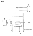
- the diamond film is deposited on an Si substrate using a microwave plasma assisted CVD apparatus, as shown in Fig. 1.
- reaction gas is introduced through a gas-feeding pipe 4 into a reactor 7.
- Microwave oscillated by a magnetron 1 is transmitted through a waveguide 2 and is introduced into reactor 7 from a quartz vacuum window 3.
- the microwave excites the reaction gas to generate microwave plasma 10 on Si substrate 11.
- the light emitted from microwave plasma 10 is transmitted through a monitoring window 8 and is spectroscopically measured by a spectroscope 9.
- a stage 12 on which substrate 11 is supported includes a water-cooling mechanism, and thus the temperature of the substrate can arbitrarily be controlled irrespective of the state of plasma. Formation conditions of the diamond film in the present example were as follows.
- the microwave-inputting power was set to be 1kW, 3kW and 5kW, to form a diamond film on a Si substrate having a diameter of 2 inches.
- the emitted light in a visible radiation range of microwave plasma was spectroscopically measured by a spectroscope, and the result thereof is shown in Fig. 2.
- the band spectrum of C 2 molecule was observed together with Balmer lines of an H atom.
- Fig. 3 shows an enlarged view of an emission band of C 2 molecule having a vibration level difference of +1, which is observed in the wavelength range between 465 and 475 nm.
- the vibration temperature may also be obtained using the spectrum shown in Fig. 4 where the difference in the vibration levels is zero.
- Fig. 4 is an enlarged view of the wavelength range between 470 and 530 nm of the spectrum shown in Fig. 2.
- A vibration temperature of the carbon molecule
- B film deposition rate of diamond
- C full width at half maximum of diamond peak (1333 cm -1 ) due to Raman spectroscopy, which is a baseline of the quality of diamond, were obtained.
- the obtained values are shown in Table 1 for the central and peripheral portions of the substrate.
- Microwave-inputting power (kW) Central portion of substrate Peripheral portion of substrate Vibration temp.
- the vibration temperature can be controlled by adjusting the microwave-inputting power. Moreover, it was proved that there is a close correlation between (a) vibration temperature, (b) film deposition rate of diamond and (c) Raman FWHM.
- a diamond film is deposited with the vibration temperature within a range between 2400 and 2700 K, a high quality diamond film with good crystallinity having Raman FWHM of 5.0 cm -1 or lower can be obtained.
- the Si substrate is dissolved by an acid mixture containing hydrofluoric acid and nitric acid (HNO 3 + HF) to obtain a diamond self-supported film.
- the diamond film is distributed from the central portion to the peripheral portion, showing transmittance of 71 %, which is close to the theoretical transmittance, from ultraviolet to infrared regions.
- example 1 described above used methane as a carbon source, acetylene, benzene, ethanol, or the mixture thereof may also be used to obtain a similar result.
- a diamond film was deposited with the conditions indicated below using the microwave plasma assisted CVD apparatus shown in Fig. 1 that was used in the example 1.
- a diamond film was formed using the conditions indicated below with constant microwave-inputting power of 3 kW and changing pressure in the reactor.
- the pressure in the reactor was set to be at 10.7 kPa, 13.3 kPa and 16.0 kPa, to form a diamond film on an Si substrate having a diameter of 2 inches.
- the vibration temperature of C 2 molecule was obtained for each pressure in the reactor.
- the pressure in the reactor, the film deposition rate (of diamond), and Raman FWHM were obtained for each of the central and peripheral portions of the substrate. The result is shown in Table 2.
- the vibration temperature can also be controlled by changing the pressure in the reactor. From the relation between the vibration temperature and the Raman FWHM, it is recognized that a high quality diamond film having the Raman FWHM of 5.0 cm -1 could be formed when the vibration temperature of C 2 molecule was set to be within the range between 2400 and 2700 K. This diamond film is transparent from ultraviolet to infrared regions. Furthermore, it was proved that a diamond film having a thermal conductivity of 1000 W/m ⁇ K or higher applicable to a heat sink or the like could be obtained if the diamond film was formed with a temperature within a range between 2200 and 2800 K. Pressure in reactor (kPa) Central portion of substrate Peripheral portion of substrate Vibration temp.
- the vibration temperature of a carbon molecule may be obtained in the following manner: an arithmetic unit is connected to spectroscope 9 shown in Fig. 1 and an integral of the intensity in a certain wavelength or of the intensity in the proximity including the certain wavelength is obtained. Subsequently, the arithmetic operation represented by the equation (3) is performed in the arithmetic unit, to obtain a vibration temperature of a carbon molecule.
Landscapes
- Chemical & Material Sciences (AREA)
- General Chemical & Material Sciences (AREA)
- Chemical Kinetics & Catalysis (AREA)
- Engineering & Computer Science (AREA)
- Materials Engineering (AREA)
- Mechanical Engineering (AREA)
- Metallurgy (AREA)
- Organic Chemistry (AREA)
- Inorganic Chemistry (AREA)
- Crystals, And After-Treatments Of Crystals (AREA)
- Chemical Vapour Deposition (AREA)
Abstract
Description
wherein sccm stands for standard cubic centimeter per minute.
| Microwave-inputting power (kW) | Central portion of substrate | Peripheral portion of substrate | ||||
| Vibration temp. (K) | Deposition rate (µm/hr) | Raman FWHM (cm-1) | Vibration temp. (K) | Deposition rate (µm/hr) | Raman FWHM (cm-1) | |
| 1 | 2200 | 1.0 | 5.5 | 1600 | 0.2 | 10.5 |
| 3 | 2700 | 1.5 | 4.5 | 2400 | 1.3 | 5.0 |
| 5 | 3000 | 1.7 | 8.5 | 2850 | 1.6 | 6.5 |
| Pressure in reactor (kPa) | Central portion of substrate | Peripheral portion of substrate | ||||
| Vibration temp. (K) | Deposition rate (µm/hr) | Raman FWHM (cm-1) | Vibration temp. (K) | Deposition rate (µm/hr) | Raman FWHM (cm-1) | |
| 10.7 | 2100 | 0.9 | 6.5 | 2000 | 0.8 | 8.5 |
| 13.3 | 2700 | 1.5 | 4.5 | 2400 | 1.3 | 5.0 |
| 16.0 | 3200 | 2.2 | 11.5 | 2600 | 1.4 | 5.5 |
Claims (8)
- A method of forming a diamond film, wherein a gas mixture of hydrocarbon gas and hydrogen gas is introduced into a reactor (7), and said gas mixture is excited by microwaves introduced into said reactor to generate a plasma, thereby forming a diamond film on a substrate (11), said method comprising the steps of:spectroscopically measuring light emitted from said plasma; andcontrolling a formation condition of said diamond film such that a spectrum of a carbon molecule (C2) measured in said spectroscopic measuring step falls within a predetermined range.
- The method according to claim 1, wherein said formation condition is controlled such that said spectrum of the carbon molecule (C2) is an emission spectrum band of the carbon molecule and that a vibration temperature obtained from said emission spectrum band falls within a predetermined range.
- The method according to claim 2, wherein said formation condition is controlled such that said vibration temperature of the carbon molecule (C2) falls within a range of from 2000 to 2800 K.
- The method according to any one of claims 1 to 3, wherein at least one of microwave-inputting power, pressure in the reactor and flow rate of reaction gas in said formation condition of the diamond film is controlled such that said spectrum falls within a predetermined range.
- The method according to any one of claims 2 to 4, wherein said vibration temperature of the carbon molecule is obtained from a spectrum band having a difference of + 1 or - 1 between a high vibration level and a low vibration level.
- The method according to any one of claims 2 to 5, wherein said vibration temperature is obtained using said emission spectrum band of the carbon molecule (C2) within a wavelength range of from 465 to 475 nm.
- A film-forming apparatus for forming a diamond film, the apparatus comprising:a reactor (7) in which reaction gas is excited by microwaves to generate a plasma (10);a microwave generating device (1) for generating said microwaves;a spectroscope (9) for generating a spectrum of light emitted from said plasma; andan arithmetic unit for obtaining a vibration temperature from an emission spectrum band of a carbon molecule (C2) obtained by said spectrometer.
- The film-forming apparatus according to claim 7, further comprising:
control means for controlling at least one of microwave-inputting power, pressure in the reactor, and flow rate of the reaction gas, such that the vibration temperature falls within a predetermined range, based on a value of said vibration temperature obtained by said arithmetic unit.
Applications Claiming Priority (2)
| Application Number | Priority Date | Filing Date | Title |
|---|---|---|---|
| JP2000170739 | 2000-06-07 | ||
| JP2000170739A JP2001354492A (en) | 2000-06-07 | 2000-06-07 | Method and apparatus for forming diamond film |
Publications (3)
| Publication Number | Publication Date |
|---|---|
| EP1162285A2 true EP1162285A2 (en) | 2001-12-12 |
| EP1162285A3 EP1162285A3 (en) | 2004-11-03 |
| EP1162285B1 EP1162285B1 (en) | 2006-09-20 |
Family
ID=18673406
Family Applications (1)
| Application Number | Title | Priority Date | Filing Date |
|---|---|---|---|
| EP01304981A Expired - Lifetime EP1162285B1 (en) | 2000-06-07 | 2001-06-07 | Method and apparatus for forming diamond film |
Country Status (5)
| Country | Link |
|---|---|
| US (2) | US6458415B2 (en) |
| EP (1) | EP1162285B1 (en) |
| JP (1) | JP2001354492A (en) |
| CA (1) | CA2348397C (en) |
| DE (1) | DE60123169T2 (en) |
Families Citing this family (13)
| Publication number | Priority date | Publication date | Assignee | Title |
|---|---|---|---|---|
| US7155475B2 (en) * | 2002-02-15 | 2006-12-26 | Sony Corporation | System, method, and computer program product for media publishing request processing |
| US7173334B2 (en) * | 2002-10-11 | 2007-02-06 | Chien-Min Sung | Diamond composite heat spreader and associated methods |
| US7351285B2 (en) * | 2005-03-29 | 2008-04-01 | Tokyo Electron Limited | Method and system for forming a variable thickness seed layer |
| US7749564B2 (en) * | 2005-03-31 | 2010-07-06 | Caterpillar Inc. | Method and apparatus for the production of thin film coatings |
| US7791188B2 (en) | 2007-06-18 | 2010-09-07 | Chien-Min Sung | Heat spreader having single layer of diamond particles and associated methods |
| JP2009059798A (en) * | 2007-08-30 | 2009-03-19 | Sumitomo Electric Ind Ltd | Method for manufacturing diamond electronic device |
| US8747963B2 (en) * | 2009-01-23 | 2014-06-10 | Lockheed Martin Corporation | Apparatus and method for diamond film growth |
| US8778784B2 (en) | 2010-09-21 | 2014-07-15 | Ritedia Corporation | Stress regulated semiconductor devices and associated methods |
| US9006086B2 (en) | 2010-09-21 | 2015-04-14 | Chien-Min Sung | Stress regulated semiconductor devices and associated methods |
| CN103221180A (en) | 2010-09-21 | 2013-07-24 | 铼钻科技股份有限公司 | Superabrasive tools with substantially flat particle tips and related methods |
| GB201121655D0 (en) * | 2011-12-16 | 2012-01-25 | Element Six Ltd | Substrates for semiconductor devices |
| CN104903490B (en) | 2012-08-30 | 2017-11-07 | 二A科技有限公司 | Apparatus and method for producing diamond and performing real-time in situ analysis |
| JP6292244B2 (en) * | 2016-03-01 | 2018-03-14 | トヨタ自動車株式会社 | Film forming method and plasma enhanced chemical vapor deposition apparatus |
Family Cites Families (10)
| Publication number | Priority date | Publication date | Assignee | Title |
|---|---|---|---|---|
| US4011521A (en) * | 1967-02-16 | 1977-03-08 | Avco Corporation | High powered laser |
| US4407705A (en) * | 1981-05-14 | 1983-10-04 | The United States Of America As Represented By The Secretary Of The Air Force | Production of negative ions of hydrogen |
| KR960016218B1 (en) * | 1987-06-05 | 1996-12-07 | 가부시기가이샤 히다찌세이사꾸쇼 | Surface treatment method and apparatus |
| JPH08757B2 (en) * | 1988-12-26 | 1996-01-10 | 住友電気工業株式会社 | Diamond and its vapor phase synthesis method |
| US5118378A (en) * | 1989-10-10 | 1992-06-02 | Hitachi, Ltd. | Apparatus for detecting an end point of etching |
| US5201986A (en) | 1990-08-07 | 1993-04-13 | Sumitomo Electric Industries, Ltd. | Diamond synthesizing method |
| JPH0492890A (en) | 1990-08-07 | 1992-03-25 | Sumitomo Electric Ind Ltd | Diamond synthesis method |
| US5518759A (en) * | 1993-07-28 | 1996-05-21 | Applied Science And Technology, Inc. | High growth rate plasma diamond deposition process and method of controlling same |
| KR100276736B1 (en) * | 1993-10-20 | 2001-03-02 | 히가시 데쓰로 | Plasma processing equipment |
| TW524888B (en) * | 2000-02-01 | 2003-03-21 | Winbond Electronics Corp | Optical temperature measurement as an in-situ monitor of etch rate |
-
2000
- 2000-06-07 JP JP2000170739A patent/JP2001354492A/en active Pending
-
2001
- 2001-06-04 US US09/873,620 patent/US6458415B2/en not_active Expired - Fee Related
- 2001-06-05 CA CA002348397A patent/CA2348397C/en not_active Expired - Fee Related
- 2001-06-07 EP EP01304981A patent/EP1162285B1/en not_active Expired - Lifetime
- 2001-06-07 DE DE60123169T patent/DE60123169T2/en not_active Expired - Lifetime
-
2002
- 2002-08-16 US US10/222,085 patent/US6837935B2/en not_active Expired - Fee Related
Also Published As
| Publication number | Publication date |
|---|---|
| CA2348397A1 (en) | 2001-12-07 |
| DE60123169D1 (en) | 2006-11-02 |
| JP2001354492A (en) | 2001-12-25 |
| US6837935B2 (en) | 2005-01-04 |
| US20030000467A1 (en) | 2003-01-02 |
| EP1162285B1 (en) | 2006-09-20 |
| EP1162285A3 (en) | 2004-11-03 |
| CA2348397C (en) | 2008-09-02 |
| US20020005170A1 (en) | 2002-01-17 |
| US6458415B2 (en) | 2002-10-01 |
| DE60123169T2 (en) | 2007-09-13 |
Similar Documents
| Publication | Publication Date | Title |
|---|---|---|
| US4394237A (en) | Spectroscopic monitoring of gas-solid processes | |
| US6837935B2 (en) | Microwave plasma film-forming apparatus for forming diamond film | |
| Elliott et al. | Optical emission spectroscopic studies of microwave enhanced diamond CVD using CH4/CO2 plasmas | |
| US9139909B2 (en) | Microwave plasma reactors | |
| Goyette et al. | Swan band emission intensity as a function of density | |
| Fan et al. | Ultraviolet laser photolysis of hydrocarbons for nondiamond carbon suppression in chemical vapor deposition of diamond films | |
| Klages | Chemical vapor deposition of diamond | |
| Lombardi et al. | Spectroscopic diagnostics and modeling of Ar∕ H2∕ CH4 microwave discharges used for nanocrystalline diamond deposition | |
| WO1995012013A1 (en) | Diamond film growth from fullerene precursors | |
| US20020005159A1 (en) | Method of producing thin semiconductor film and apparatus therefor | |
| Sergeichev et al. | Atmospheric-pressure microwave plasma torch for CVD technology of diamond synthesis | |
| Tristant et al. | Microwave plasma enhanced CVD of aluminum oxide films: OES diagnostics and influence of the RF bias | |
| Petherbridge et al. | Molecular beam mass spectrometry investigations of low temperature diamond growth using CO2/CH4 plasmas | |
| JP2000109366A (en) | Light non-transmittive high purity silicon carbide material, light shieldable material for semiconductor treating device, and semiconductor treating device | |
| Okada et al. | Measurement of C2 rotational temperature in Ar-SiH4-CH4 inductively coupled plasma flame with Abel inversion | |
| Okada et al. | Analysis of optical emission spectra from ICP of Ar–SiH4–CH4 system | |
| JP2885547B2 (en) | Method for producing silicon dioxide thin film | |
| Berghaus et al. | Local growth studies of CVD diamond using a probe-like substrate | |
| Chen et al. | Gas phase study and oriented self-standing diamond film fabrication in high power DC arc plasma jet CVD | |
| JP3319550B2 (en) | Deposition method of polycrystalline Si thin film | |
| Gennett et al. | Laser Synthesis of Single-wall Carbon Nanotubes Utilizing High Temperature Induction Heating. | |
| GB2700698A (en) | Microwave plasma reactor and method of operation | |
| Benndorf et al. | Fundamental Gas Processes for the CVD Diamond Growth from H2/C2/H2/O2 and Ar/C2H2/O2 Mixtures | |
| JP3093836B2 (en) | Diamond film fabrication method | |
| ORR-ERWING | Pulsed and continuous wave cavity ring-down spectroscopy probes of chemical vapour deposition plasmas |
Legal Events
| Date | Code | Title | Description |
|---|---|---|---|
| PUAI | Public reference made under article 153(3) epc to a published international application that has entered the european phase |
Free format text: ORIGINAL CODE: 0009012 |
|
| AK | Designated contracting states |
Kind code of ref document: A2 Designated state(s): AT BE CH CY DE DK ES FI FR GB GR IE IT LI LU MC NL PT SE TR |
|
| AX | Request for extension of the european patent |
Free format text: AL;LT;LV;MK;RO;SI |
|
| PUAL | Search report despatched |
Free format text: ORIGINAL CODE: 0009013 |
|
| AK | Designated contracting states |
Kind code of ref document: A3 Designated state(s): AT BE CH CY DE DK ES FI FR GB GR IE IT LI LU MC NL PT SE TR |
|
| AX | Request for extension of the european patent |
Extension state: AL LT LV MK RO SI |
|
| 17P | Request for examination filed |
Effective date: 20041022 |
|
| 17Q | First examination report despatched |
Effective date: 20050426 |
|
| AKX | Designation fees paid |
Designated state(s): DE FR GB |
|
| GRAP | Despatch of communication of intention to grant a patent |
Free format text: ORIGINAL CODE: EPIDOSNIGR1 |
|
| GRAS | Grant fee paid |
Free format text: ORIGINAL CODE: EPIDOSNIGR3 |
|
| GRAA | (expected) grant |
Free format text: ORIGINAL CODE: 0009210 |
|
| AK | Designated contracting states |
Kind code of ref document: B1 Designated state(s): DE FR GB |
|
| REG | Reference to a national code |
Ref country code: GB Ref legal event code: FG4D |
|
| REF | Corresponds to: |
Ref document number: 60123169 Country of ref document: DE Date of ref document: 20061102 Kind code of ref document: P |
|
| ET | Fr: translation filed | ||
| PLBE | No opposition filed within time limit |
Free format text: ORIGINAL CODE: 0009261 |
|
| STAA | Information on the status of an ep patent application or granted ep patent |
Free format text: STATUS: NO OPPOSITION FILED WITHIN TIME LIMIT |
|
| 26N | No opposition filed |
Effective date: 20070621 |
|
| PGFP | Annual fee paid to national office [announced via postgrant information from national office to epo] |
Ref country code: FR Payment date: 20100709 Year of fee payment: 10 |
|
| PGFP | Annual fee paid to national office [announced via postgrant information from national office to epo] |
Ref country code: DE Payment date: 20100602 Year of fee payment: 10 Ref country code: GB Payment date: 20100602 Year of fee payment: 10 |
|
| GBPC | Gb: european patent ceased through non-payment of renewal fee |
Effective date: 20110607 |
|
| REG | Reference to a national code |
Ref country code: FR Ref legal event code: ST Effective date: 20120229 |
|
| REG | Reference to a national code |
Ref country code: DE Ref legal event code: R119 Ref document number: 60123169 Country of ref document: DE Effective date: 20120103 |
|
| PG25 | Lapsed in a contracting state [announced via postgrant information from national office to epo] |
Ref country code: DE Free format text: LAPSE BECAUSE OF NON-PAYMENT OF DUE FEES Effective date: 20120103 Ref country code: FR Free format text: LAPSE BECAUSE OF NON-PAYMENT OF DUE FEES Effective date: 20110630 |
|
| PG25 | Lapsed in a contracting state [announced via postgrant information from national office to epo] |
Ref country code: GB Free format text: LAPSE BECAUSE OF NON-PAYMENT OF DUE FEES Effective date: 20110607 |