EP1161116A2 - Optical switch with connection verification - Google Patents
Optical switch with connection verification Download PDFInfo
- Publication number
- EP1161116A2 EP1161116A2 EP01304669A EP01304669A EP1161116A2 EP 1161116 A2 EP1161116 A2 EP 1161116A2 EP 01304669 A EP01304669 A EP 01304669A EP 01304669 A EP01304669 A EP 01304669A EP 1161116 A2 EP1161116 A2 EP 1161116A2
- Authority
- EP
- European Patent Office
- Prior art keywords
- optical
- signals
- output
- input
- ports
- Prior art date
- Legal status (The legal status is an assumption and is not a legal conclusion. Google has not performed a legal analysis and makes no representation as to the accuracy of the status listed.)
- Granted
Links
Images






Classifications
-
- H—ELECTRICITY
- H04—ELECTRIC COMMUNICATION TECHNIQUE
- H04Q—SELECTING
- H04Q11/00—Selecting arrangements for multiplex systems
- H04Q11/0001—Selecting arrangements for multiplex systems using optical switching
- H04Q11/0005—Switch and router aspects
-
- H—ELECTRICITY
- H04—ELECTRIC COMMUNICATION TECHNIQUE
- H04Q—SELECTING
- H04Q11/00—Selecting arrangements for multiplex systems
- H04Q11/0001—Selecting arrangements for multiplex systems using optical switching
- H04Q11/0005—Switch and router aspects
- H04Q2011/0007—Construction
- H04Q2011/0015—Construction using splitting combining
-
- H—ELECTRICITY
- H04—ELECTRIC COMMUNICATION TECHNIQUE
- H04Q—SELECTING
- H04Q11/00—Selecting arrangements for multiplex systems
- H04Q11/0001—Selecting arrangements for multiplex systems using optical switching
- H04Q11/0005—Switch and router aspects
- H04Q2011/0037—Operation
- H04Q2011/0043—Fault tolerance
-
- H—ELECTRICITY
- H04—ELECTRIC COMMUNICATION TECHNIQUE
- H04Q—SELECTING
- H04Q11/00—Selecting arrangements for multiplex systems
- H04Q11/0001—Selecting arrangements for multiplex systems using optical switching
- H04Q11/0062—Network aspects
- H04Q2011/0079—Operation or maintenance aspects
- H04Q2011/0083—Testing; Monitoring
-
- H—ELECTRICITY
- H04—ELECTRIC COMMUNICATION TECHNIQUE
- H04Q—SELECTING
- H04Q11/00—Selecting arrangements for multiplex systems
- H04Q11/0001—Selecting arrangements for multiplex systems using optical switching
- H04Q11/0062—Network aspects
- H04Q2011/0084—Quality of service aspects
Definitions
- the present invention relates generally to communications networks employing wavelength division multiplexed optical signals and, more particularly, to methods and systems for enabling the verification of individual switch connections established by large optical switches used in such networks.
- FIG. 1 shows an example of an optical switch 100, adapted to receive a plurality of wavelength division multiplexed (WDM) input signals S IN,A ...S IN,N on a respective plurality of input optical fibers 110A...110N and adapted to output a corresponding set of WDM output signals S OUT,A ...S OUT,N on a respective plurality of output optical fibers 120A...120N.
- WDM wavelength division multiplexed
- WDM wavelength division demultiplexing
- WDM devices 130 A ...130 N for splitting up respective ones of the WDM input signals S IN,A ...S IN,N into their single-carrier components.
- WDM devices 140A...140N for recombining respective sets of single-carrier optical signals into the WDM output signals S OUT,A ...S OUT,N , respectively.
- a switching core 150 Disposed between the WDD devices 130A...130N and the WDM devices 140A...140N is a switching core 150, which provides switching functionality for the array of single-carrier optical signals arriving from the WDD devices 130A...130N.
- the switching core 150 is responsive to a connection map provided by a switch controller 160 which interfaces with network components that are external to the optical switch 100.
- the switching activity performed by the switching core 150 may occur in the electrical domain (with the aid of opto-electronic converters) or in the optical domain or in a combination of the two.
- optical switches are known as photonic switches.
- the switching core 250 of the photonic switch 200 provides controllable switching of the single-carrier optical signals received from the WDD devices 130A...130N.
- the switching core 250 comprises M optical switch matrices 210A...210M, one for each of the M optical wavelengths in the system, as well as a wavelength converting switch 220.
- Each of the optical switch matrices 210A...210M has a fixed number of input ports and output ports and can (but need not) be a Micro-Electro-Mechanical System (MEMS) device similar in concept to, or as described in "Free-Space Micromachined Optical-Switching Technologies and Architectures" by Lih Y. Lin of AT&T Labs-Research during OFC99 Session W14-1 on February 24, 1999.
- MEMS Micro-Electro-Mechanical System
- a MEMS device comprises a set of mirrors that are arranged in geometrical relationship with the input and output ports in such a way that incoming light from any input port can be diverted to any output port by raising an appropriate one of the mirrors.
- the raising and lowering of mirrors is performed under control of the switch controller 160.
- each of the optical switch matrices 210A...210M has a total of K+N input ports and K+N output ports where N is the number of WDM input signals and WDM output signals.
- N is the number of WDM input signals and WDM output signals.
- each of the N input ports is connected to the like-wavelength output port of a respective one of the WDD devices 130A...130N, while the remaining K input ports are connected to the wavelength converting switch 220.
- the signals exiting the optical switch matrices 210A...210M through the output ports thereof can be referred to as "switched" single-carrier optical signals and are shown at 260 in Fig. 2.
- switched single-carrier optical signals exiting a particular one of the switching matrices 210A...210M N of these are fed to like-wavelength input ports of the WDM devices 140A...140N, while the remaining K signals are fed to the wavelength converting switch 220.
- the wavelength converting switch 220 thus receives and outputs MxK single-carrier optical signals.
- the wavelength converting switch 220 is equipped with circuitry for converting the received single-carrier optical signals into electronic form, electrically switching the electronic signals and then modulating each switched electronic signal in accordance with an optical source at a desired wavelength.
- Wavelength conversion is particularly useful when an input wavelength is already in use along the fiber path leading to a destination WDM device. It is also useful as a regeneration function when the optical signal has accumulated too many impairments for onward direct optical propagation.
- Fig. 2 permits optical signals of a given wavelength entering any particular optical switch matrix (associated with a particular wavelength) to be connected in a non-blocking fashion to any like-wavelength input port on any of the WDM devices 140A...140N. Moreover, provided sufficient switching capacity is provided in the wavelength converting switch 220, the wavelength of a number of single-carrier optical signals can be changed so that each of these signals may appear on any input port of any of the WDM devices 140A...140N.
- the wavelength converting switch 220 may accept a plurality of add carriers on a plurality (R) of "add” paths 280 and similarly may output a plurality of drop carriers on a plurality (R) of "drop” paths 270.
- the term “wavelength converting switch” will be used throughout the following, with the understanding that a “wavelength converting switch” may have either wavelength conversion capabilities or add/drop capabilities or both.
- the switch controller 160 generates a connection map under external or locally generated stimulus and provides this connection map to the components of the switching core 250. Specifically, each optical switch matrix executes a respective (N+K) x (N+K) mapping in the optical domain and the wavelength converting switch 220 executes an (MxK) x (MxK) mapping in the electrical domain.
- Another consequence of the increasing density of emerging high-capacity WDM systems is an increased probability with which the switching of single-carrier optical signals within the optical switch 100 can be made erroneously or, in some cases, not made at all.
- Some of the myriad causes of mis-connections and lost connections include stuck or failed switch elements in the switching core 150, hardware or software failures causing incorrect switch path instructions to be received by the switching core 150 from the switch controller 160, human error (e.g., a mis-connected fiber interconnect into or between bays of switching equipment), etc.
- the present invention is directed to enabling connection verification in an optical switch that has a switching core that performs at least part of its switching directly in the optical domain in response to a connection map.
- the switch is equipped with a set of optical intensity controllers at its input, where one intensity controller is associated with each input optical fiber. Each of the intensity controllers is controllably driven to vary a corresponding WDM input traffic signal with a low power test signal.
- the switch is also equipped with optical splitters at its output in order to recover a portion of the power of each WDM output signal, which can then be optically demultiplexed, thus affording visibility into the set of single-carrier optical signals which exit the switching core. If, in addition to purely optical switching, wavelength conversion is provided within the switching core, then additional optical splitters may be provided at the input to the wavelength conversion unit, thereby to provide full visibility of all of the single-carrier optical signals being switched by the switching core.
- the switch is further equipped with a path integrity analyzer connected to the splitters and to the intensity controllers.
- the path integrity analyzer generates or controls generation of the test signals applied by the intensity controllers.
- the path integrity analyzer also receives the tapped portions of the WDM output signals and separates them into their single-carrier components in order to recover the set of switched single-carrier optical signals.
- the path integrity analyzer is further provided with test signal detectors used to detect the presence of a test signal in each recovered switched single-carrier optical signal.
- the path integrity analyzer can thus ascertain the integrity of the connection involving each switched single-carrier optical signal by comparing the detected test signal to an expected test signal that is derived from the connection map.
- the path integrity analyzer since the path integrity analyzer has knowledge of the test signals and the WDM input signals to which the test signals are being applied, and since the path integrity analyzer also has knowledge of the connection map which is supposed to be applied by the switching core, the path integrity analyzer can determine which test signal, if any, is supposed to appear in each of the given switched single-carrier optical signal.
- the invention may be summarized according to a first broad aspect as a switch for optical signals, including a plurality of wavelength division demultiplexers, each having an input port and a plurality of output ports; a plurality of wavelength division multiplexers, each having an output port and a plurality of input ports; an optical switching core having a plurality of input ports and a plurality of output ports, at least some of the input ports of the optical switching core being connected to the output ports of the wavelength division demultiplexers and at least some of the output ports of the optical switching core being connected to the input ports of the wavelength division multiplexers, the optical switching core being capable of establishing wavelength-preserving connections between its input ports and its output ports in response to receipt of a connection map; a plurality of optical intensity controllers, each being adapted to vary the intensity of an input wavelength division multiplexed optical signal entering the input port of a corresponding one of the wavelength division demultiplexers; a plurality of optical splitters, each being adapted to tap a fraction of the optical power of an output wavelength division
- connection verification unit is operable to control the optical intensity controllers so as to cause the application of a test signal to each input wavelength division multiplexed optical signal.
- the connection verification unit is further operable to process the output wavelength division multiplexed optical signals tapped by the splitters in order to determine which test signal, if any, appears in each of the signals exiting the at least some of the output ports of the optical switching core.
- the connection verification unit is operable to determine whether the wavelength-preserving connections involving the signals entering the at least some of the input ports and the signals exiting the at least some of the output ports of the optical switching core have been established in accordance with the connection map.
- connection verification system including the above-mentioned optical intensity controllers, optical splitters and connection verification unit.
- the invention may be summarized as a method of validating the switch connections established by the switching core, including: varying a property of each first wavelength division multiplexed optical signal in accordance with a corresponding test signal; tapping and optically demultiplexing the second wavelength division multiplexed signals, thereby to access the at least some of the wavelength division multiplexed optical signals present at the second ports of the switching core, such signals being called "switched optical signals"; for each switched optical signal, determining which, if any, test signal appears in that switched optical signal; and for each switched optical signal, comparing the test signal found to be present in that switched optical signal to an expected test signal corresponding to that switched optical signal.
- the invention may be summarized according to a further broad aspect as a path integrity analyzer for use in verifying the integrity of connections made by an optical switch, includiing: a controller for controlling the application of test signals to the first wavelength division multiplexed optical signals; a wavelength separation stage for demultiplexing the second wavelength division multiplexed optical signals into component signals, thereby to access the at least some of the optical signals present at the second ports of the switching core, such signals being called "switched optical signals"; a detection stage for determining which test signal, if any, appears in each switched optical signal; and the controller being further adapted to compare, for each switched optical signal, the test signal found to be present in that switched optical signal to an expected test signal corresponding to that switched optical signal.
- a plurality of optical splitters may be provided for tapping those switched optical signals travelling from output ports of the optical switching core to input ports of the wavelength conversion unit.
- the control unit may further be operable to determine whether the wavelength-preserving connections involving the signals entering the at least some of the input ports of the optical switching core and the signals exiting those output ports of the optical switching core that are connected to the wavelength conversion unit have been established in accordance with the connection map.
- a plurality of optical intensity controllers may also be positioned so that they vary the intensity of the optical signal entering a corresponding one of the input ports of the optical switching core that are connected to the wavelength conversion unit.
- the control unit may further be operable to determine whether the wavelength-preserving connections involving the optical signals entering those input ports of the optical switching core that are connected to the wavelength conversion unit and the signals exiting the at least some of the output ports of the optical switching core have been established in accordance with the connection map.
- a mechansim constructed and adapted to remove the test signals from the signals exiting the output ports of the optical switching core prior to recombination at the wavelength division multiplexing devices.
- the present invention is directed to providing connection verification for a photonic switch, i.e., an optical switch that is capable of making direct optical connections without requiring wavelength conversion.
- a photonic switch i.e., an optical switch that is capable of making direct optical connections without requiring wavelength conversion.
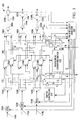
- Fig. 3 shows an embodiment of a photonic switch 300 equipped with connection verification functionality.
- the switch 300 in Fig. 3 is based on the switch 200 in Fig. 2 and thus retains the WDD devices 130A...130N, the WDM devices 140A...140N and the switching core including the optical switch matrices 210A...210M and the wavelength converting switch 220.
- the components of the switch 200 which have been retained in the switch 300 could be exactly as described in the background section or they could be any functional or structural equivalents or improvements thereupon.
- the present invention enables verification of the connections made by each of the M optical switch matrices 210A...210M. This includes “type 1" connections (between the WDD devices 130A...130N and the WDM devices 140A...140N) , “type 2" connections (between the WDD devices 130A...130N and the wavelength converting switch 220) and “type 3" connections (between the wavelength converting switch 220 and the WDM devices 140A...140N).
- the switch 300 is equipped with a set of N optical intensity controllers 320A...320N, a set of MxK optical intensity controllers 325 A,A ...325 M,K , a set of N asymmetric optical splitters 330A...330N, a set of MxK asymmetric optical splitters 340 A,A ...340 M,K and a path integrity analyzer 350.
- a modified switch controller 310 is also provided.
- optical intensity controllers 320A...320N and the optical splitters 330A...330N are together used for verifying "type 1" connections (i.e., those between the WDD devices 130A...130N and the WDM devices 140A...140N), while the optical intensity controllers 320A...320N and the optical splitters 340 A,A ...340 M,K are together used for verifying "type 2" connections (i.e., those between the WDD devices 130A...130N and the wavelength converting switch 220).
- optical intensity controllers 325 A,A ...325 M,K and the optical splitters 330A...330N are together used for verifying "type 3" connections (i.e., those between the wavelength converting switch 220 and the WDM devices 140A...140N).
- the N optical intensity controllers 320A...320N are respectively placed in the optical paths of the WDM input signals travelling along the input optical fibers 110A...110N.
- the MxK optical intensity controllers 325 A,A ...325 M,K are respectively placed in the optical paths of the single-carrier optical signales travelling between the wavelength converting switch 220 and the optical switch matrices 210A...210M.
- Each optical intensity controller can be of standard design and includes circuitry and control logic for varying the intensity of the corresponding optical signal in accordance with a test signal received from the path integrity analyzer 350.
- a particular test signal will have a property that uniquely identifies the optical signal with which it is associated.
- each of the WDM input signals on the input optical fibers 110A...110N is associated with a unique test signal.
- each WDM input signal is "tagged" by its own test signal and the combination of test signal and wavelength uniquely identifies each input single-carrier optical signal.
- each of the MxK single-carrier optical signals travelling between the wavelength converting switch 220 and the optical switch matrices 210A...210M is tagged by its own test signal.
- the test signals may be constant-amplitude carriers at unique frequencies.
- each of the test signals may consist of the sum of two or more constant-amplitude carriers at a unique pair of frequencies.
- the test signals may be a constant-frequency carriers unique amplitudes or unique phases.
- the test signals may consist of carriers modulated with unique duty cycles or unique digital message words, for example.
- the choice of carriers used in a test signal can influence the accuracy and speed with which these carriers are later detected.
- the carrier frequencies should be chosen in such a frequency range and with such a degree of proximity in frequency as to suit the operational requirements of the invention.
- the amplitude of each test signal should be sufficiently low compared to the amplitude of the corresponding optical signal whose intensity it modulates.
- the modulation depth should be kept to below a few percent of the peak optical power and it may be beneficial to remove the test signal before leaving the switch 300, depending on the optical link design. Embodiments of the invention which provide removal of the test signals are discussed in greater detail later on.
- each of the N asymmetric optical splitters 330A...330N is placed in the optical path of a respective WDM output signal travelling along a respective one of the output optical fibers 120A...120N. It is to be understood that the optical splitters 330A...330N may be placed following a respective plurality of amplifiers 240A...240N (as shown) or preceding the amplifiers 240A...240N. Although there is virtually no difference in performance of the path integrity analyzer 350, selection of one embodiment over the other may be made for the purposes of enhancing compatibility of the connection verification system with the optical switch described in U.S. Patent Application serial no. 09/580,495 to Graves et al., entitled “Optical Switch with Power Equalization", filed on May 30, 2000, assigned to the assignee of the present invention and hereby incorporated by reference herein.
- the other MxK asymmetric optical splitters 340 A,A ...340 M,K are placed in the optical path of those switched optical signals 260 that lead from the optical switch matrices 210A...210M to the wavelength converting switch 220.
- the relatively small number (i.e., N+(MxK)) optical splitters 330A...330N, 340 A,A ...340 M,K provide visibility of all of the Mx(N+K) switched single-carrier optical signals 260 at the N+K output ports of each of the M optical switch matrices 210A...210M.
- Each asymmetric optical splitter can be of standard design and is constructed so as to allow a small percentage of light arriving along the corresponding optical path to be branched off towards the path integrity analyzer 350.
- a suitable amount of optical power tapped in this manner will be 10 dB to 13 dB below the optical power level of the incoming signal, which lowers the optical power level of the ongoing signal by only 0.46 dB to 0.22 dB, respectively.
- each of the asymmetric optical splitters 330A...330N located at the output of the switch can also be constructed so as to allow a small percentage of light arriving along the corresponding optical path to be branched off towards a power spectrum equalization system (or "equalizer") as described in above-referenced U.S. Patent Application serial no. 09/580,495. This would permit integration of a power equalization system together with a connection verification system.
- a power spectrum equalization system or "equalizer”
- the switch controller 310 provides a connection map to the optical switch matrices 210A...210M and provides another connection map to the wavelength converting switch 220. These connection maps are also provided to the path integrity analyzer 350.
- the switch controller 310 further receives integrity information from the path integrity analyzer 350 in a suitable format.
- the switch controller 310 is similar to the switch controller 160 in the switch 200 of Fig. 2 but is additionally equipped with the capability to supply the path integrity analyzer 350 with connection maps and with the capability to handle integrity information received from the path integrity analyzer 350.
- the integrity information can be processed by the switch controller 310 or may be supplied in unmodified form to other network components external to the switch 300.
- the path integrity analyzer 350 is seen to comprise a path integrity analysis controller (PIAC) 410 connected to the optical intensity controllers 320A...320N, to the optical intensity controllers 325 A,A ...325 M,K and to a front end unit 430.
- the PIAC 410 will be described in more detail later on and is basically responsible for producing the test signals which modulate the WDM input signals and the single-carrier optical signals travelling between the wavelength converting switch 220 and the optical switch matrices 210A...210M.
- the PIAC 410 is also responsible for reading the test signals detected by the front end unit 430 and for validating connections by comparing detected test signals to "expected" test signals.
- the path integrity analyzer 350 can fill any or all of three major roles: verification, diagnostic and servicing.
- the verification mode consists of confirming the presence or absence of the correct test signal in each switched single-carrier optical signal.
- the diagnostic mode pinpoints, in the event that an incorrect test signal is found to appear in a particular switched single-carrier optical signal, the source of such mis-connection.
- the servicing (signal-trace) mode can be entered upon external request from a user of a particular single-carrier optical signal (270 or 260) and who may require information about the connection involving that particular signal.
- the front end unit 430 is responsible for detecting the test signal on each of the switched single-carrier optical signals 260 (see Fig. 3).
- the N WDM signals tapped by the splitters 330A...330N and the MxK single-carrier signals tapped by the splitters 340 A,A ...340 M,K provide the front end unit 430 with complete visibility of all the switched single-carrier optical signals 260.
- test signal detection may or may not be performed simultaneously on all the switched single-carrier optical signals 260, depending on the design of the front end unit 430 as seen herein below.
- the PIAC 410 may supply a select signal to a multiplexer in the front end unit 430 which selects only one of the currently available detected test signals. This select signal is hereinafter denoted (P,Q), where P and Q are used to identify the Pth output port of the Qth optical switch matrix 210Q.
- Which switched single-carrier optical signals 260 form part of the "currently available" subset may depend solely on P or solely on Q or on both P and Q, depending on the internal structure of the front end unit 430.
- the internal structure of the front end unit 430 affects the time required to obtain a reliable version of the detected test signal for each combination of P and Q. Individual designers may opt for different trade-offs in these two respects.
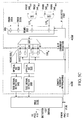
- the front end unit 430 is seen to comprise a wavelength separation stage 430W and a detection stage 430D.
- the wavelength separation stage has a set of N M-output WDD devices 520, one for each of the N WDM signals tapped by the splitters 330A...330N.
- Each of the M output ports of each of the N WDD devices 520, as well as each of the splitters 340 A,A ...340 M,K is connected to a respective one of a plurality of optical receivers 530.
- Mx(N+K) optical receivers 530 there are Mx(N+K) optical receivers 530, one for each of the Mx(N+K) switched single-carrier optical signals 260, which means that the "currently available" subset includes the entire set of switched single-carrier optical signals 260.
- Each of the optical receivers 530 comprises circuitry for transforming the corresponding received optical signal into electronic form.
- the optical receivers perform an envelope detection function rather than a high-speed data detection function and thus need only have an electrical bandwidth larger than the highest frequency of any test signal.
- Each of the optical receivers 530 is connected to a respective one of a plurality of test signal detectors 540.
- Each of the test signal detectors 540 comprises suitable circuitry, software and/or control logic for detecting the presence of a test signal in the signal received from the respective optical receiver 530.
- Each test signal detector produces a detected test signal which may be fed directly to the PIAC 410 or, as shown, can be fed to a multiplexer 510A of standard design. The detected test signal indicates which test signal appears in the signal being processed by the corresponding test signal detector 540.
- Each test signal detector 540 needs to extract a "clean" test signal which, as already mentioned, may consist of a carrier, a group of carriers or a carrier modulated with a digital message word, for example. To do this successfully, a test signal detector may need to detect very small variations in the envelope of the signal received from the corresponding optical receiver. However, the low-frequency components of the signal so received will be contaminated with low-frequency components of the traffic data stream, which act as a powerful interference source to corrupt the detection of the test signal. Fortunately, the low frequency components behave as a band-limited white noise source and hence are amenable to mitigation in much the same way as a white noise interference source.
- each test signal detector could contain a high-Q narrowband tuned filter set to the center frequency of that carrier.
- synchronous detection can be used in the test signal detectors 540, whereby the output of the high-Q narrowband filter is heterodyned with a sample of the expected carrier, in which case the spectral component of the resultant signal will produce a static d.c. signal, whereas other noise contributions (except that in the final smoothing circuit for the d.c. filter) will be eliminated. This permits a virtually zero-bandwidth measurement with a low noise component and high confidence.
- test signal is a pair of carriers
- two such high-Q narrowband tuned filters could be used.
- the bandwidth of the low-pass filter used in filtering the homodyne beat signal would be set above the actual digital modulation bandwidth of the digital message word.
- the maximal message data rate of a 32-bit word would be on the order of 10 kb/s, while can readily be accommodated through a 5 kHz channel and therefore a low pass filter with a 5 kHz cut-off could be used.
- the multiplexer 510A will have Mx(N+K) data input ports.
- the multiplexer 510A also has a control port which is driven by the select signal (denoted (P,Q)) received from the PIAC 410 and which uniquely identifies the optical switch matrix and output port of a particular switched single-carrier optical signal.
- the multiplexer 510A of Fig. 5A could be dispensed with if the PIAC 410 has Mx(N+K) parallel ports. In this case; processing of the output of each test signal detector 540 could be purely under software control of the PIAC 410.
- the multiplexer 510 (and others like it in Figs. 5B through 5D) could be implemented in software, hardware or a combination of the two.
- the "currently available" subset for the front end unit of Fig. 5A is the entire set of Mx(N+K) switched single-carrier optical signals 260, a reliable version of the detected test signal for each combination of P and Q is available at any time and thus the test signal detectors 540 do not require an additional "settling time” other than an initial settling time interval.
- the absence of settling effects in the duration of the detection cycle comes at the expense of a high component count, since the front end unit of Fig. 5A requires the use of Mx(N+K) optical receivers 530 and a like number of test signal detectors 540.
- the optical receivers only need have very narrow bandwidth and hence are likely to be available in low cost arrays, and likewise the test signal detectors 540 are likely to be available in an integrated multi-detector-per-ASIC form, the sheer number of receivers and test signal detectors may in some cases make this approach more expensive, bulky or power hungry than desired.
- FIG. 5B there is shown an embodiment of a front end unit 430 which dramatically reduces the required number of optical receivers 530 and test signal detectors 540 to M each.
- the wavelength separation stage 430W comprises an optical switch matrix 550, which could be (but is not restricted to being) a MEMS device such as described in the above-referenced article by Lih Y. Lin.
- the optical switch matrix 550 receives the N WDM signals tapped by the splitters 330A...330N as well as K WDM signals 570A...570K which are derived from having selectively re-combined the MxK single-carrier signals tapped by the splitters 340 A,A ...340 M,K into K groups.
- K WDM signals 570A...570K K WDM signals
- optical switch matrix 550 Among the output ports of the optical switch matrix 550, only one need be used and is connected to an M-output WDD device 520 much like the one in Fig. 5A.
- An array of mirrors 555 in the optical switch matrix 550 can be raised or lowered to deflect any specific input onto the output in accordance with a control signal.
- the control signal associated with the Qth optical switch matrix 210Q specifies the Pth input port of that optical switch matrix.
- Each output port of the M-output WDD device 520 is connected to a respective one of a plurality of optical receivers 530 in the detection stage 430D.
- the optical receivers 530 can be identical to the optical receivers suitable for use in the embodiment of Fig. 5A.
- Fig. 5B it is seen that there are M optical receivers 530, which means that the "currently available" subset includes only M out of Mx(N+K) switched single-carrier optical signals 260, which correspond to all the wavelengths on one specific, selected output port.
- This approach may be referred to as the "output-port-sequential-summing" (OPSS) approach.
- the front end unit 430 has to be stepped through N+K phases or configurations, by a process of raising or lowering individual mirrors 555. This process will lead to a corresponding slowdown of the overall verification process.
- Each of the optical receivers 530 is connected to a respective one of a plurality of test signal detectors 540, which can be identical to any of the test signal detectors suitable for use in the embodiment of Fig. 5A.
- each test signal detector 540 comprises suitable circuitry, software and/or control logic for detecting the presence of a test signal in the signal received from the respective optical receiver 530.
- Each of the M test signal detectors 540 produces a detected test signal which is fed to the PIAC 410 either directly or, as shown, via a multiplexer 510B.
- the multiplexer 510B needs to have only M data input ports, one for each of the M switched single-carrier optical signals in the "currently available" subset which, in the OPSS approach, corresponds to all M wavelengths on one specific, selected output port.
- the multiplexer 510B also has a control port which is driven by the portion of the select signal from the PIAC 410 which contains the identity of the Qth wavelength (out of a possible M wavelengths).
- T SETTLE is used to denoted the settling time, i.e., the time it takes for a connection integrity verification detector to begin producing a reliable measurement
- ⁇ is used to denoted the total number of switched single-carrier optical signals (in this case Mx(N+K)) divided by the size of the "currently available" subset
- the total settling time will be equal to ⁇ x T SETTLE .
- the "settling time” (denoted T SETTLE ) depends on the switching time of the MEMS switch as well as the carrier frequencies selected as test signals and, in the case of modulated carrier, on the modulated carriers' data rates.
- FIG. 5C there is shown another embodiment of the front end unit 430 where the number of optical receivers 530 and test signal detectors 540 has been reduced to H each (where H is equal to 2 in the embodiment of Fig. 5C).
- This reduced complexity is achieved by providing an optical switch matrix 550 for receiving the N WDM signals tapped by the splitters 330A...330N and the K WDM signals 570A...570K formed in the previously described manner, combined with a second set of optical switch matrices 550' 1 ...550' H for selection of individual optical carriers.
- the array of mirrors 555 in the optical switch matrix 550 can be raised or lowered in accordance with a control signal which is again the portion of the select signal which identifies the selected output port, denoted P.
- the M output ports of the M-output WDD device 520 are recombined in groups by a set of H optical switch matrices 550' 1 ...550' H , among which only two are shown in Fig. 5C.
- the value of H is determined by the practical switch sizes available and the number of parallel sets of test signal detectors 540 and optical receivers 530 required to achieve an adequate connection verification response time. Therefore the required number of sets of test signal detectors and optical receivers is determined by the response time requirements of the verification system, while the number and size of the optical switch matrices 550' 1 ...550' H is determined by the number of sets of test signal detectors and optical receivers.
- each optical switch matrix 550' can be raised or lowered in accordance with a subgroup selection signal which is equal to Q div H (i.e., the number of times Q divides H).
- An output port of each of the optical switch matrices 550' is connected to a respective one of a like number of optical receivers 530.
- the size of the "currently available" subset is equal to the number of optical receivers 530, which is equal to H.
- Each of the optical receivers 530 is connected to a respective one of a plurality of test signal detectors 540, which can be identical to any of the test signal detectors suitable for use in the embodiments of Figs. 5A and 5B.
- each test signal detector 540 comprises suitable circuitry, software and/or control logic for detecting the presence of the test signal in the signal received from the respective optical receiver 530.
- Each of the test signal detectors 540 produces a detected test signal which is fed to a data input port of a multiplexer 510C.
- the multiplexer 510C has only H data input ports and also has a select port which is driven by a subgroup interleaving signal received which is equal to Q mod H, i.e., the remainder after dividing Q by H.
- Fig. 5D shows another alternative embodiment of the front end unit, wherein a total of N+K tunable optical filters 590 are provided, each of which receives either a respective one of the N WDM signals tapped by the splitters 330A...330N or a respective one of K WDM signals 570A...570K formed in the previously described manner.
- Each tunable optical filter may be of standard design and may comprise circuitry for admitting the portion of the power of the received optical signal contained in a controllable optical passband.
- the optical passband is controllable in accordance with the portion of the select signal which specifies Q, corresponding to the selected optical switch matrix 210Q.
- Each of the tunable optical filters 590 is connected to a respective one of a plurality of optical receivers 530.
- N+K optical receivers 530 which means that the "currently available" subset includes only N+K out of the Mx(N+K) switched single-carrier optical signals 260.
- Each of the optical receivers 530 is connected to a respective one of a plurality of test signal detectors 540, which can be identical to any of the test signal detectors suitable for use in the embodiments of Figs. 5A, 5B and 5C.
- each of the N+K test signal detectors 540 comprises suitable circuitry, software and/or control logic for detecting the presence of the test signal in the signal received from the respective optical receiver 530.
- Each of the N+K test signal detectors 540 produces a detected test signal which is fed to a data input port of a multiplexer 510D.
- the multiplexer 510D has N+K data input ports, one for each of the N+K switched single-carrier optical signals in the "currently available" subset.
- the multiplexer 510D also has a select port which is driven by the portion of the select signal from the PIAC 410 that identifies P, the selected output port of the Qth optical switch matrix 210Q.
- FIG. 5E Another embodiment of the front end unit 430 is shown in Fig. 5E, where there is provided a single optical switch matrix 550 connected to a single tunable optical filter 590, which is connected to a single wide-optical-bandwidth receiver 530, which is in turn connected to a single test signal detector 540. No multiplexer is required in this embodiment.
- the optical switch matrix 550 receives the N WDM signals tapped by the splitters 330A...330N as well as the K WDM signals 570A...570K formed in the previously described manner.
- P is provided to the optical switch matrix 550 and Q is provided to the tunable optical filter 590. While the embodiment of Fig. 5E is clearly the most efficient in terms of component usage, it has a longer detection cycle time due to settling. This is due to the fact that the test signal detector 540 must start its detection operation "from scratch" each time either P or Q is changed in the select signal (P,Q) received from the PIAC 410. Thus, the detection cycle time due to settling will equal (Mx(N+K)) x T SETTLE .
- Fig. 7A shows the general results for arbitrary M, N, K and average T SETTLE .
- M 40 wavelengths
- N 24 input optical fibers
- K 8 wavelength conversion input/output ports per optical switch matrix
- H 4.
- optical switch matrices 550, 550' in the front end unit 430 are (N+K)-input optical switch matrices, then it is possible to integrate these optical switch matrices with the optical switch matrices 210A...210M in the switching core 250.
- additional slots not only for use with spare optical switch matrix cards but also for use with the optical switch matrix cards 550, 550' needed by the front end unit 430.
- the respective multiplexer could be dispensed with, in which case multiple detected test signals could be supplied simultaneously to different input ports of the PIAC 410.
- Figs 5A-5E has shown how the PIAC 410 can be provided with the detected test signal resulting from the front end unit 430 having performed a test signal detection operation on a particular single-carrier optical signal which is uniquely specifiable by the values of P (output port) and Q (wavelength) in the select signal (P,Q) .
- the role of the PIAC 410 is then to compare each detected test signal with an "expected" test signal in order to determine whether there is consistency with the connection map.
- the PIAC 410 may be implemented as circuitry, software, control logic or a combination thereof. To permit operation in more than one mode from among verification, diagnostic and servicing, the software or hardware resources of the PIAC 410 can be split up into several parts. If implemented as software, the PIAC 410 may include program code instructions stored on a computer-readable medium. The program code instructions define a connection integrity verification algorithm to be followed by the PIAC 410. The algorithm for the verification function is now described with additional reference to the flowchart in Fig. 6.
- connection verification algorithm now described refers to the verification of all "type 1", “type 2" and “type 3" connections but those skilled in the art may adapt the algorithm to the verification of any subset of these connections or any subset of connections for a given type of connection.
- the PIAC 410 produces N different test signals which are fed to the optical intensity controllers 320A...320N.
- the PIAC 410 also produces MxK different test signals which are fed to the optical intensity controllers 325 A,A ⁇ 325 M,K ⁇
- the PIAC 410 determines which test signal has been detected on each of the switched single-carrier optical signals 260. To determine which test signal appears in the particular switched single-carrier optical signal associated with the Pth output port of the Qth optical switch matrix 210Q, the PIAC 410 sends a select signal (containing the values of P and Q) to the front end unit 430.
- the detected test signal contains a unique carrier frequency for each combination of P and Q.
- the detected test signal contains a unique pair of carrier frequencies, denoted f OUT,P,Q,1 and f OUT,P,Q,2 , for each combination of P and Q.
- the detected test signal contains a unique digital message word for each combination of P and Q.
- the PIAC 410 reads and stores the unique property of the detected test signal in local memory, for example in an array structure. In one specific embodiment, there may be one (N+K)-element array per optical switch matrix, with each element containing the identity of two detected frequencies.
- the PIAC 410 cycles through all values of P and Q and thus determines the test signal appearing in each of the switched single-carrier optical signals 260.
- a counter and parallel bus structure may be used. Each bit of the counter could be a separate line on the bus and the current value of P may be taken as the most significant bits on the bus, while the current value of Q can be taken as the remaining bits on the bus.
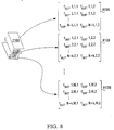
- each array from a set of arrays 810A...810M is associated with a respective one of the optical switch matrices 210A...210M.
- the nth row of the array associated with a particular optical switch matrix contains the two frequencies thought to be contained in the switched single-carrier optical signal emerging from the n th port of that optical switch matrix.
- the n th row of the m th array 810m contains two elements denoted f OUT,n,m,Z , for Z ⁇ ⁇ 1, 2 ⁇ . It is recalled that "n” ranges from A...N+K and "m" ranges from A...M.
- each detected test signal is processed by the PIAC 410 in order to determine whether it corresponds to an "expected" test signal, namely the test signal that would have been detected if the connection maps of the optical switch matrices 210A...210M and the wavelength converting switch 220 were executed properly.
- an "expected" test signal corresponding to a particular output port on a particular optical switch matrix (i.e., corresponding to a particular value of P and Q) can be derived from the connection map of each optical switch matrix as provided by the switch controller 310.
- a separate verification operation can be performed for each of the arrays 810A...810M (i.e., for each optical switch matrix), by comparing each element of the array to an "expected" carrier frequency.
- connection verification algorithm may enter the diagnostic mode at step 640, where the PIAC 410 searches for the source of the faulty connection.
- connection verification functionality in a photonic switch.
- the uses of such functionality are many and varied, and include status reporting, protection switching, performance monitoring, testing, and so on.
- complete visibility of all the signals being switched by all of the optical switch matrices 210A...210M is provided by a system with a relatively small number of components, including a path integrity analyzer, N optical intensity controllers and N+(MxK) asymmetric optical splitters.
- the system of the present invention adds considerable functionality at reasonably low additional cost.
- the same test signal could be used for all optical signals but in a sequential manner.
- a demultiplexer in the PIAC 410 so that the test signal could be routed to a selected one of the optical intensity controllers 320A...320N, 325 A,A ...325 M,K . Consequently, a complete detection cycle would require (N + MxK) passes for the entire range of P and Q, one pass being required for each time a different WDM input signal is selected to be modulated with the test signal.
- the verification process at the PIAC 410 is (N + MxK) times more computationally intense, as a comparison operation is performed for each combination of test signal and switched single-carrier optical signal.
- the test signal detectors 540 can be simplified, as they need only conclude the presence or the absence of one single test signal in the switched single-carrier optical signal they are currently processing. To enhance detection accuracy, the test signal itself may be supplied from the PIAC 410 to the test signal detectors 540, thereby to serve as a reference signal.
- the electronic signals produced by the optical receivers 530 can be used not only for connection verification but also for other purposes such as power estimation.
- the functionality of the test signal detectors 540 may be enhanced to include other capabilities such as power estimation as described in more detail in above-referenced U.S. Patent Application serial no. 09/580,495. Therefore, it is within the scope of the present invention to allow hardware sharing in order to provide dual functionality, i.e., connection verification functionality and power estimation functionality.
- the set of MxK optical splitters 340 A,A ...340 M,K intercepts the single-carrier optical signals travelling from the optical switch matrices 210A...210M to the wavelength converting switch 220.
- the splitters 340 A,A ...340 M,K it is possible to avoid the need for the splitters 340 A,A ...340 M,K if the electrical counterparts to these signals are tapped directly from within the wavelength converting switch 220.
- the wavelength converting switch 220 consists of a plurality of opto-electronic converters, an electrical switch and a plurality of electro-optic converters
- the output of each opto-electronic converter provides an electrical signal which can be used by the test signal detector(s) 540 in the front end unit 430.
- the electrical signals received from the wavelength converting switch 220 will be high-speed signals and may need to undergo an envelope detection step before processing by the connection integrity verification detectors, but this may be acceptable, given the elimination of the splitters 340 A,A ...340 M,K and the optical receivers 530 from the front end unit 430.
- the PIAC 410 can generate a diagnostic select signal which causes a second optical signal to appear at a second output port of the optical switch matrices 550 of Figs. 5B, 5C and 5E.
- the second signal is different from the one currently exiting the first output port by virtue of the current value of the select signal.
- the second optical signal can be referred to as a diagnostic signal and may be converted, demodulated and processed by a diagnostic controller which can be merged with the PIAC 410.
- the diagnostic controller may run a sophisticated troubleshooting algorithm in parallel with the connection integrity verification algorithm of the PIAC 410 previously described with reference to Fig. 6.
- test signals applied to a particular WDM input signal or to a particular single-carrier optical signal entering an optical switch matrix via the wavelength converting switch 220 remain on the optical signal after switching.
- the signals which propagate out of the switch 300 onto output optical fibers 140A...140N will have optical intensities that are modulated with test signals. This phenomenon occurs during the connection verification process which may run continuously and thus may in some cases have an adverse effect on the performance of downstream equipment. Since it is expected that there will be multiple switches in a photonic network and since the modulation will propagate out of the switch on the optical carriers to the next switch, the path integrity check system of one switch could interfere with the path integrity check system of the next switch unless certain preventative measures are taken.
- the signal leaving the optical switch will consist of WDM streams in which each of the individual optical carriers will have a few percent amplitude modulation at uncorrelated test signal frequencies.
- These frequencies if onwardly propagated to downstream nodes, could prevent these nodes from using the same set of test signal frequencies, forcing the planning of test signal frequencies to be effected at the level of the network, rather than at the level of each node. This may limit the flexibility of the network and the size it can grow to before the restriction in the number of available carriers and/or the complexity of the test signal detector to discriminate ever more tightly packed carriers becomes a limiting factor.
- the present invention provides at least two methods can be used to avoid interference to downstream network equipment, namely (1) suppressing the onward propagation of the carriers by removing the test signals and (2) using a test signal that does not cause interference with the operation of the next switch down the line.
- the first of these methods can be implemented by introducing anti-phase modulation of the same test signal carriers at a place near the output, but before the final WDM device (since the output carriers passing through that multiplexer could have come from any input and hence will contain a variety of test signal carriers).
- This can be achieved by introducing an additional gain adjustment point immediately prior to the WDM device, in the form of an EDFA (Erbium Doped Fiber Amplifier) array.
- EDFA Erbium Doped Fiber Amplifier
- the use of the EDFA for this purpose may be combined with the use of the EDFA to control the power spectrum of the WDM signals output by the switch, as described in above-referenced U.S. Patent Application serial no. 09/580,495.
- the anti-phase signal can be derived from the detection stage in the front end unit 430 by tapping the output of each receiver 530 and passing this signal through an inverting amplifier.
- the closed loop from the EDFAs through the WDM devices 140A...140N, through the splitters 330A...330N and back through the wavelength separation stage in the front end unit 430 creates a self-adjusting compensation block that reduces the level of the residual output carrier to the detection threshold of the test signal detector.
- complete cancellation can be used whenever a particular wavelength is not being tested which, for the scanning versions of the front end 430, will be the case during an overwhelming majority of the time.
- the second of the above methods is best suited to test signals that consist of a digital word modulated onto a carrier.
- different switches would simply use different carrier frequencies, although the carrier frequency impressed onto all inputs of the same switch would be the same, with the digital carrier modulation serving as the differentiator between the various inputs.
- the use of a simple repetitive 32-bit word would allow up to 2 32 (approximately 10 10 ) switch inputs, while the interference between switch sites would be eliminated by allocating each switch site a different analog carrier frequency.
- the example frequency plan shown earlier (between 1 MHz and 6 MHz) would allow for up to 20 switches to coexist in a network without interference issues.
- a fixed passband receiver say ⁇ 50kHz
- up 50 channels i.e., 50 switches
- other frequency plans and channelization widths are possible to permit higher counts, although narrowing receiver bandwidth may extend the settling time required before reliable measurements are available.
- the optical switching could be performed by switch fabrics other than those based on MEMS devices, for example liquid crystal switching fabrics, bubble (total internal reflection) switching fabric, thermo-optic switching fabrics, etc.
- switch fabrics other than those based on MEMS devices, for example liquid crystal switching fabrics, bubble (total internal reflection) switching fabric, thermo-optic switching fabrics, etc.
- the chosen switch fabric has the possibility of establishing an erroneous connection such that a signal on one wavelength is connected into an outgoing connection intended for another wavelength, then this error will not be detectable by the use of a connection verification signal as contemplated herein since the wavelength would not be interpreted as incorrect. Therefore, the present invention is best suited for use in optical switches where there are no physical paths between wavelength planes, although there may be mis-connections within each individual wavelength plane.
Landscapes
- Engineering & Computer Science (AREA)
- Computer Networks & Wireless Communication (AREA)
- Optical Communication System (AREA)
- Use Of Switch Circuits For Exchanges And Methods Of Control Of Multiplex Exchanges (AREA)
Abstract
Description
Claims (40)
- A switch for optical signals, comprising:a plurality of wavelength division demultiplexers (WDDs), each having an input port and a plurality of output ports;a plurality of wavelength division multiplexers (WDMs), each having an output port and a plurality of input ports;an optical switching core having a plurality of input ports at which optical signals enter said core and a plurality of output ports at which optical signals exit said core, a subset of the input ports of said core being connected to the output ports of said WDDs and a subset of the output ports of said core being connected to the input ports of said WDMs, said core being capable of establishing photonic connections between said subset of its input ports and said subset of its output ports in response to an indication of desired connections;a plurality of optical intensity controllers, each connected to the input port of a corresponding one of said WDDs and adapted to vary the intensity of an input multi-carrier optical signal entering the input port of said corresponding one of said WDDs;a plurality of optical splitters, each connected to the output port of a corresponding one of said WDMs and adapted to tap a fraction of the intensity of an output multi-carrier optical signal exiting the output port of said corresponding one of said WDMs; anda connection verification unit connected to said optical intensity controllers and to said optical splitters, said connection verification unit being operable to:(a) control said optical intensity controllers so as to cause a test signal to be applied to at least one of the input multi-carrier optical signals;(b) determine, on the basis of at least one of the desired connections and for at least one of the signals exiting said subset of the output ports of said core, which test signal is expected to appear in said at least one of the signals exiting said subset of the output ports of said core;(c) process the output multi-carrier optical signals tapped by said optical splitters in order to detect which test signal, if any, appears in said at least one of the signals exiting said subset of the output ports of said core; and(d) compare the detected and expected test signals, thereby determining whether said at least one of the desired connections has been correctly established by said core.
- A switch as claimed in claim 1, wherein the connection verification unit comprises:a first stage, for separating the output multi-carrier optical signals tapped by said optical splitters into single-carrier component signals corresponding to said at least one of the signals exiting said subset of the output ports of said core;a second stage connected to the first stage, for detecting test signals appearing in said single-carrier component signals; anda third stage connected to the second stage, for comparing the test signals detected in said single-carrier component signals to the test signals expected to appear in the corresponding signals exiting said subset of the output ports of said core.
- A switch as claimed in claim 2, wherein the second stage is further operable to convert each single-carrier component signal into an electrical signal prior to detecting the test signals appearing in said single-carrier component signals.
- A switch as claimed in claim 3, wherein each electrical signal has a data bandwidth narrower than that of the single-carrier component signal from which it is obtained.
- A switch as claimed in claim 2, wherein said first stage comprises a plurality of second WDDs, each having a respective plurality of output ports and having a respective input port connected to a respective one of the optical splitters.
- A switch as claimed in claim 5, wherein the second stage comprises:a plurality of optical receivers, each receiver having an output port and having an input port connected to a corresponding one of the output ports of one of the second WDDs; anda plurality of test signal detectors, each test signal detector having an output port and having an input port connected to a respective one of the optical receivers.
- A switch as claimed in claim 2, wherein said first stage comprises a plurality of tunable optical filters, each having an output port and having an input port connected to a respective one of the optical splitters, each tunable optical filter being adapted to admit an optical signal in a selected optical frequency range through to said second stage.
- A switch as claimed in claim 7, wherein the connection verification unit comprises a controller for controlling application of the test signals by the intensity controllers and for selecting the optical frequency range admitted by at least one tunable optical filter.
- A switch as claimed in claim 7, wherein the second stage comprises:a plurality of optical receivers, each receiver having an output port and having an input port connected to the output port of a corresponding one of the tunable optical filters; anda plurality of test signal detectors, each test signal detector having an output port and having an input port connected to a respective one of the optical receivers.
- A switch as claimed in claim 2, wherein the first stage comprises:an optical switching element having an output port and having a plurality of input ports respectively connected to the optical splitters, said optical switching element being arranged to admit an optical signal appearing on a selected one of its input ports through to its output port; anda second WDD having a plurality of output ports and having an input port connected to the output port of said optical switching element.
- A switch as claimed in claim 10, wherein the connection verification unit comprises a controller for controlling application of the test signals by the intensity controllers and for selecting the input port of the optical switching element on which appears the optical signal admitted to the output port of the optical switching element.
- A switch as claimed in claim 10, wherein the second stage comprises:a plurality of optical receivers, each having an output port and having an input port connected to a corresponding one of the output ports of said second WDD; anda plurality of test signal detectors, each having an output port and having an input port connected to a corresponding one of said optical receivers.
- A switch as claimed in claim 2, wherein the first stage comprises:a first optical switching element having an output port and having a plurality of input ports respectively connected to the optical splitters, said optical switching element being adapted to pass an optical signal appearing on a selected one of its input ports through to its output port; anda second WDD having a plurality of output ports and having an input port connected to the output port of said first optical switching element; andat least one second optical switching element connected to the output ports of said second WDD, each said at least one second optical switching element having an output port, said at least one second optical switching element having an aggregate number of input ports sufficient to accommodate the output ports of said WDD, each said second optical switching element being adapted to pass an optical signal appearing on a selected one of its input ports through to its output port.
- A switch as claimed in claim 13, wherein the connection verification unit comprises a controller for controlling application of the test signals by the intensity controllers and for selecting the input port of the optical switching element on which appears the optical signal admitted to the output port of each first and second optical switching element.
- A switch as claimed in claim 13, wherein the second stage comprises:at least one optical receiver, each having an output port and having an input port connected to a corresponding one of said at least one second optical switching element; andat least one test signal detector, each having an output port and having an input port connected to a corresponding one of said at least one optical receiver.
- A switch as claimed in claim 2, wherein the first stage comprises:an optical switching element having an output port and having a plurality of input ports respectively connected to the optical splitters, said optical switching element being arranged to admit an optical signal appearing on a selected one of its input ports through to its output port; anda tunable optical filter connected to the output port of said optical switching element, said tunable optical filter being adapted to admit an optical signal in a selected optical frequency range through to said second stage.
- A switch as claimed in claim 16, wherein the connection verification unit comprises a controller for controlling application of the test signals by the intensity controllers and for selecting the optical frequency range admitted by said tunable optical filter.
- A switch as claimed in claim 16, wherein the second stage comprises:an optical receiver having an ouptut and having an input connected to said tunable optical filter; anda test signal detector connected to said optical receiver.
- A switch as claimed in claim 2, said core comprising a plurality of optical switching elements, each said optical switching element having a plurality of input ports and a plurality of output ports and operable to establish photonic connections therebetween, wherein a subset of the input ports of said optical switching elements represents said subset of the input ports of the core and wherein a subset of the output ports of said optical switching elements represents said subset of the output ports of the core.
- A switch as claimed in claim 19, further comprising a wavelength converting switch, said wavelength converting switch having a plurality of input ports and a plurality of output ports and operable to establish non-photonic connections therebetween, wherein the input ports of the wavelength converting switch are connected to output ports of the core which are not members of said subset of the output ports of the core and wherein the output ports of the wavelength converting switch are connected to input ports of the core which are not members of said subset of the input ports of the core.
- A switch as claimed in claim 20, further comprising a plurality of second optical splitters connected to the output ports of the core which are not members of said subset of the output ports of the core.
- A switch as claimed in claim 21, wherein the first stage comprises:a plurality of second WDMs, each having an output port and having a plurality of input ports connected to the second optical splitters;an optical switching element having an output port and having a plurality of input ports each connected to a corresponding one of the first optical splitters or to a corresponding one of the output ports of one of the second WDMs, said optical switching element being arranged to admit an optical signal appearing on a selected one of its input ports through to its output port; anda second WDD having a plurality of output ports and having an input port connected to the output port of said optical switching element.
- A switch as claimed in claim 22, wherein the first stage further comprises:
at least one second optical switching element connected to the output ports of said second WDD, each said at least one second optical switching element having an output port, said at least one second optical switching element having an aggregate number of input ports sufficient to accommodate the output ports of said WDD, each said second optical switching element being adapted to pass an optical signal appearing on a selected one of its input ports through to its output port. - A switch as claimed in claim 23, wherein the second stage comprises:a plurality of first optical receivers, each having an output port and having an input port connected either to a corresponding one of the second optical splitters or to a corresponding one of the output ports of one of the second WDDs;a plurality of first test signal detectors, each first test signal detector having an output port and having an input port connected to a respective one of the optical receivers;at least one second optical receiver, each having an output port and having an input port connected to the output port of a corresponding one of said at least one second optical switching element in the first stage; anda second test signal detector having an output port and having an input port connected to the output of the second optical receiver.
- A switch as claimed in claim 21, wherein the first stage comprises:a plurality of second WDMs, each having an output port and having a plurality of input ports connected to the second optical splitters;an optical switching element having an output port and having a plurality of input ports each connected to a corresponding one of the first optical splitters or to a corresponding one of the output ports of one of the second WDMs, said optical switching element being arranged to admit an optical signal appearing on a selected one of its input ports through to its output port; anda tunable optical filter connected to the output port of said optical switching element, said tunable optical filter being adapted to admit an optical signal in a selected optical frequency range through to said second stage.
- A switch as claimed in claim 25, wherein the second stage comprises:an optical receiver having an output port and having an input port connected to the output port of the tunable optical filter; anda test signal detector having an output port and having an input port connected to a the optical receiver.
- A switch as claimed in claim 2, further comprising a power spectrum equalization unit connected to said first stage and utilizing said single-carrier component signals corresponding to said at least one of the signals exiting said subset of the output ports of said core.
- A switch as claimed in claim 1, wherein test signals applied to different ones of the input multi-carrier optical signals have mutually distinct amplitudes or frequency content or encode mutually distinct digital messages.
- A switch as claimed in claim 1, further comprising a test signal cancellation unit for removing at least one test signal from at least one of optical signals exiting said subset of the output ports of the core.
- A switch as claimed in claim 29, wherein said at least one test signal is a frequency tone and wherein said test signal cancellation unit comprises an anti-phase modulator.
- A switch as claimed in claim 30, wherein said anti-phase modulator is adapted to derive anti-phase modulation by tapping said at least one test signal from said connection verification unit and passing the at least one tapped signal through an inverting amplifier.
- A switch as claimed in claim 2, wherein the test signals applied to at least two different input multi-carrier optical signals are mutually non-interfering.
- A system for use with a switch for optical signals, the switch having a plurality of wavelength division demultiplexers (WDDs), each having an input port and a plurality of output ports; a plurality of wavelength division multiplexers (WDMs), each having an output port and a plurality of input ports; and an optical switching core having a plurality of input ports at which optical signals enter the core and a plurality of output ports at which optical signals exit the core, wherein a subset of the input ports of the core is connected to the output ports of the WDDs and wherein a subset of the output ports of the core is connected to the input ports of the WDMs, the core being capable of establishing photonic connections between the subset of its input ports and the subset of its output ports in response to an indication of desired connections, the system comprising:a plurality of optical intensity controllers, each connectable to the input port of a corresponding one of the WDDs and adapted to vary the intensity of an input multi-carrier optical signal entering the input port of the corresponding one of the WDDs;a plurality of optical splitters, each connectable to the output port of a corresponding one of the WDMs and adapted to tap a fraction of the optical intensity of an output multi-carrier optical signal exiting the output port of the corresponding one of the WDMs; anda connection verification unit connected to said optical intensity controllers and to said optical splitters and being operable to:(a) control said optical intensity controllers so as to cause a test signal to be applied to at least one of the input multi-carrier optical signals;(b) determine, on the basis of at least one of the desired connections and for at least one of the signals exiting said subset of the output ports of said core, which test signal is expected to appear in said at least one of the signals exiting said subset of the output ports of said core;(c) process the output multi-carrier optical signals tapped by said optical splitters in order to detect which test signal, if any, appears in said at least one of the signals exiting said subset of the output ports of said core; and(d) compare the detected and expected test signals, thereby determining whether said at least one of the desired connections has been correctly established by said core.
- A connection verification unit for use with an optical switch having a switching core capable of establishing photonic connections between a plurality of input ports and a plurality of output ports in response to an indication of desired connections, wherein optical signals entering a subset of the input ports originate from a plurality of input multi-carrier optical signals and wherein optical signals exiting a subset of the output ports are recombined into a plurality of output multi-carrier optical signals, a method of determining whether at least one of the desired connections has been established by the core, comprising:a controller for controlling application of test signals to the input multi-carrier optical signals;a first stage, for separating the output multi-carrier optical signals into single-carrier component signals corresponding to the at least one of the signals exiting the subset of the output ports of the core;a second stage connected to the first stage, for detecting test signals appearing in the single-carrier component signals; anda third stage connected to the second stage, for comparing the test signals detected in the single-carrier component signals to the test signals expected to appear in the corresponding signals exiting the subset of the output ports of the core.
- A connection verification unit for use with an optical switch having a switching core capable of establishing photonic connections between a plurality of input ports and a plurality of output ports in response to an indication of desired connections, wherein optical signals entering a subset of the input ports originate from a plurality of input multi-carrier optical signals and wherein optical signals exiting a subset of the output ports are recombined into a plurality of output multi-carrier optical signals, a method of determining whether at least one of the desired connections has been established by the core, comprising:(a) means for causing a test signal to be applied to at least one of the input multi-carrier optical signals;(b) means for determining, on the basis of at least one of the desired connections and for at least one of the optical signals exiting the subset of the output ports, which test signal is expected to appear in said at least one of the optical signals exiting the subset of the output ports;(c) means for processing the output multi-carrier optical signals in order to detect which test signal, if any, appears in said at least one of the signals exiting the subset of the output ports; and(d) means for comparing the detected and expected test signals.
- In an optical switch having a switching core capable of establishing photonic connections between a plurality of input ports and a plurality of output ports in response to an indication of desired connections, wherein optical signals entering a subset of the input ports originate from a plurality of input multi-carrier optical signals and wherein optical signals exiting a subset of the output ports are recombined into a plurality of output multi-carrier optical signals, a method of determining whether at least one of the desired connections has been established by the core, comprising:(a) causing a test signal to be applied to at least one of the input multi-carrier optical signals;(b) determining, on the basis of at least one of the desired connections and for at least one of the optical signals exiting the subset of the output ports, which test signal is expected to appear in said at least one of the optical signals exiting the subset of the output ports;(c) processing the output multi-carrier optical signals in order to detect which test signal, if any, appears in said at least one of the signals exiting the subset of the output ports; and(d) comparing the detected and expected test signals.
- A method as claimed in claim 36, wherein determining the test signal expected to appear in the signal exiting a particular one of the output ports of the core comprises determining the test signal applied to the input multi-carrier optical signal from which originates the optical signal that enters the input port of the core which is defined by one of the desired connections as being connected to said particular one of the output ports of the core.
- A method as claimed in claim 37, further comprising:
if the test signal expected to appear in the signal exiting a particular one of the output ports of the core does not match the test signal, if any, appearing in the signal exiting said particular one of the output ports of the core, declaring a mis-connection and entering a diagnostic mode to localize the source of the mis-connection. - A method as claimed in claim 36, further comprising:
removing at least one test signal from at least one of the optical signals exiting said subset of the output ports of the core. - A method as claimed in claim 39, wherein at least one test signal is a frequency tones, the method further comprising:
introducing anti-phase modulation of the tone in order to effect substantial removal of said at least one test signal from said at least one of the optical signals exiting said subset of the output ports of the core.
Applications Claiming Priority (2)
| Application Number | Priority Date | Filing Date | Title |
|---|---|---|---|
| US20729200P | 2000-05-30 | 2000-05-30 | |
| US207292P | 2000-05-30 |
Publications (3)
| Publication Number | Publication Date |
|---|---|
| EP1161116A2 true EP1161116A2 (en) | 2001-12-05 |
| EP1161116A3 EP1161116A3 (en) | 2003-08-20 |
| EP1161116B1 EP1161116B1 (en) | 2006-06-21 |
Family
ID=22769926
Family Applications (1)
| Application Number | Title | Priority Date | Filing Date |
|---|---|---|---|
| EP01304669A Expired - Lifetime EP1161116B1 (en) | 2000-05-30 | 2001-05-25 | Optical switch with connection verification |
Country Status (4)
| Country | Link |
|---|---|
| US (2) | US6871021B2 (en) |
| EP (1) | EP1161116B1 (en) |
| CA (1) | CA2348121A1 (en) |
| DE (1) | DE60120838D1 (en) |
Cited By (2)
| Publication number | Priority date | Publication date | Assignee | Title |
|---|---|---|---|---|
| EP1445976A3 (en) * | 2003-02-05 | 2011-12-14 | Samsung Electronics Co., Ltd. | Wavelength path monitoring/correcting apparatus in transparent optical cross-connect and method thereof |
| CN113301456A (en) * | 2020-02-24 | 2021-08-24 | 瑞昱半导体股份有限公司 | Optical network device with abnormal light emission detection |
Families Citing this family (41)
| Publication number | Priority date | Publication date | Assignee | Title |
|---|---|---|---|---|
| US7542675B1 (en) | 2000-05-30 | 2009-06-02 | Nortel Networks Limited | Optical switch with power equalization |
| DE10036709B4 (en) * | 2000-07-27 | 2006-07-06 | Siemens Ag | Optical network node with add-drop or cross-connect functionality and associated procedures |
| US6714701B1 (en) * | 2001-05-29 | 2004-03-30 | Nortel Networks Limited | Optical switch using micromirrors and method of testing the same |
| KR100420949B1 (en) * | 2001-08-14 | 2004-03-02 | 한국전자통신연구원 | Optical switching method and system |
| US7046928B1 (en) * | 2001-09-28 | 2006-05-16 | Cisco Technology, Inc. | Link discovery and verification using loss of light |
| EP1235062B1 (en) * | 2001-11-30 | 2004-03-31 | Agilent Technologies, Inc. (a Delaware corporation) | Measurement of multi-port optical devices |
| JP2003198485A (en) * | 2001-12-28 | 2003-07-11 | Nec Corp | Cross-connect device and optical communication system |
| FR2834402B1 (en) * | 2002-01-03 | 2005-03-11 | Cit Alcatel | OPTICAL SWITCHING DEVICE AND METHOD OF CONTROLLING THE DEVICE |
| US20030133650A1 (en) * | 2002-01-16 | 2003-07-17 | Farhad Hakimi | System and method of transmitting optical signals using IIR and FIR filtration |
| US20030133649A1 (en) * | 2002-01-16 | 2003-07-17 | Farhad Hakimi | System and method of transmitting optical signals using IIR filtration |
| US6969842B2 (en) | 2002-03-29 | 2005-11-29 | Nortel Networks Limited | Dispersion discrimination for wideband optical signals |
| JP4053389B2 (en) * | 2002-09-19 | 2008-02-27 | 富士通株式会社 | Optical signal-to-noise ratio monitoring method and optical transmission system using the same |
| US7072546B2 (en) * | 2003-03-21 | 2006-07-04 | Intel Corporation | Compensation for chromatic dispersion |
| US6795601B1 (en) * | 2003-05-23 | 2004-09-21 | Agilent Technologies, Inc. | Achromatic optical switching/routing systems |
| US20090034965A1 (en) * | 2004-02-23 | 2009-02-05 | Look Christopher M | Method and an apparatus to automatically verify connectivity within an optical network node |
| US7848644B2 (en) * | 2004-02-23 | 2010-12-07 | Dynamic Method Enterprises Limited | Method and an apparatus to provide optical equipment protection |
| US7885541B2 (en) * | 2004-02-23 | 2011-02-08 | Dynamic Method Enterprises Limited | Method and apparatus for optical performance monitoring |
| US7634196B2 (en) * | 2004-10-06 | 2009-12-15 | Cisco Technology, Inc. | Optical add/drop multiplexer with reconfigurable add wavelength selective switch |
| JP4291281B2 (en) * | 2005-02-03 | 2009-07-08 | 富士通株式会社 | Information processing system, calculation node, and information processing system control method |
| US7680413B2 (en) * | 2005-05-26 | 2010-03-16 | Cisco Technology, Inc. | Optical network monitoring system and method |
| JP4625372B2 (en) * | 2005-05-26 | 2011-02-02 | 富士通株式会社 | Optical transmission device, continuity test method thereof, and optical transmission system |
| CN100504419C (en) * | 2005-06-20 | 2009-06-24 | 中国科学院半导体研究所 | Apparatus and method for testing photoelectric characteristic of thermo-optic switch array |
| US8064771B2 (en) * | 2005-06-30 | 2011-11-22 | Infinera Corporation | Active control loop for power control of optical channel groups |
| US7676155B2 (en) * | 2005-12-08 | 2010-03-09 | Electronics And Telecommunications Research Institute | Dynamic wavelength allocation device using 3R wavelength converter having limited wavelength conversion range and method thereof |
| JP2008052212A (en) * | 2006-08-28 | 2008-03-06 | Fujitsu Ltd | MEMS optical switch device |
| US8249451B2 (en) * | 2007-08-16 | 2012-08-21 | Futurewei Technologies, Inc. | Methods for characterizing optical switches and multiplexers/demultiplexers |
| US8150264B2 (en) * | 2007-11-09 | 2012-04-03 | University Of Houston | Methods for non-wavelength-converting multi-lane optical switching |
| US9490894B2 (en) * | 2008-12-08 | 2016-11-08 | Ciena Corporation | Coherent probe and optical service channel systems and methods for optical networks |
| US8433192B2 (en) * | 2008-12-08 | 2013-04-30 | Ciena Corporation | Dynamic performance monitoring systems and methods for optical networks |
| EP2609754B1 (en) * | 2010-08-25 | 2014-06-04 | Telefonaktiebolaget L M Ericsson (publ) | An optical-electrical switching node |
| JP2012244530A (en) * | 2011-05-23 | 2012-12-10 | Fujitsu Ltd | Erroneous fiber connection detection method and node device |
| CN103227758B (en) * | 2013-03-25 | 2016-01-20 | 深圳市三旺通信技术有限公司 | A kind of fiber optic Ethernet switch and control method |
| US9413520B2 (en) * | 2013-12-12 | 2016-08-09 | Ciena Corporation | Optical transceiver and method with channel binding, clock forwarding, and integrate-and-dump receivers |
| JP6406818B2 (en) * | 2013-12-13 | 2018-10-17 | 三菱電機株式会社 | Optical transmission system and optical transmission method |
| US10009671B2 (en) * | 2014-01-17 | 2018-06-26 | Tellabs Operations, Inc. | Methods and apparatus for providing configuration discovery using intra-nodal test channel |
| US10230476B1 (en) * | 2016-02-22 | 2019-03-12 | Integrated Device Technology, Inc. | Method and apparatus for flexible coherent and scale-out computing architecture |
| WO2018222740A1 (en) * | 2017-05-30 | 2018-12-06 | Commscope Technologies Llc | Reconfigurable optical networks |
| US10313021B1 (en) | 2018-01-10 | 2019-06-04 | Ciena Corporation | High-efficiency self-resetting integrating optical transceiver |
| JP7135783B2 (en) | 2018-11-27 | 2022-09-13 | 富士通株式会社 | TRANSMISSION SYSTEM, TRANSMISSION DEVICE, AND TRANSMISSION METHOD |
| CN109458874B (en) * | 2018-12-20 | 2024-02-23 | 中国人民解放军陆军工程大学 | Detection analyzer |
| US12513047B2 (en) * | 2020-12-09 | 2025-12-30 | Ntt, Inc. | Connection optimization device, connection optimization method, and program |
Family Cites Families (14)
| Publication number | Priority date | Publication date | Assignee | Title |
|---|---|---|---|---|
| US5296956A (en) * | 1992-07-17 | 1994-03-22 | At&T Bell Laboratories | Performance monitoring and fault location for optical equipment, systems and networks |
| US5867289A (en) * | 1996-12-24 | 1999-02-02 | International Business Machines Corporation | Fault detection for all-optical add-drop multiplexer |
| US6081360A (en) * | 1997-08-20 | 2000-06-27 | Fujitsu Limited | Method and apparatus for optimizing dispersion in an optical fiber transmission line in accordance with an optical signal power level |
| US5956165A (en) | 1997-09-12 | 1999-09-21 | Mci Communications Corporation | Method and apparatus for updating subcarrier modulation in a communication network |
| US6330383B1 (en) * | 1998-02-20 | 2001-12-11 | University Of Southern California | Disperson compensation by using tunable nonlinearly-chirped gratings |
| US6370300B1 (en) * | 1999-02-18 | 2002-04-09 | Lucent Technologies Inc. | Optical communication system incorporating automatic dispersion compensation modules |
| US6647208B1 (en) * | 1999-03-18 | 2003-11-11 | Massachusetts Institute Of Technology | Hybrid electronic/optical switch system |
| US6445841B1 (en) * | 1999-05-28 | 2002-09-03 | Omm, Inc. | Optomechanical matrix switches including collimator arrays |
| US6266170B1 (en) * | 1999-06-22 | 2001-07-24 | Avanex Corporation | Method and system for compensating for chromatic dispersion in an optical network |
| US6529301B1 (en) * | 1999-07-29 | 2003-03-04 | Nortel Networks Limited | Optical switch and protocols for use therewith |
| US6600581B1 (en) | 1999-08-31 | 2003-07-29 | Lucent Technologies Inc. | Connection verification in optical cross-connect arrangements |
| JP2001203637A (en) * | 2000-01-19 | 2001-07-27 | Mitsubishi Electric Corp | WDM optical transmission system |
| US6625341B1 (en) * | 2000-06-12 | 2003-09-23 | Vlad J. Novotny | Optical cross connect switching array system with electrical and optical position sensitive detection |
| US20020191247A1 (en) * | 2001-04-30 | 2002-12-19 | Xiang Lu | Fast restoration in optical mesh network |
-
2001
- 2001-05-17 CA CA002348121A patent/CA2348121A1/en not_active Abandoned
- 2001-05-18 US US09/859,544 patent/US6871021B2/en not_active Expired - Fee Related
- 2001-05-25 EP EP01304669A patent/EP1161116B1/en not_active Expired - Lifetime
- 2001-05-25 DE DE60120838T patent/DE60120838D1/en not_active Expired - Lifetime
- 2001-10-01 US US09/965,810 patent/US7039318B2/en not_active Expired - Fee Related
Cited By (3)
| Publication number | Priority date | Publication date | Assignee | Title |
|---|---|---|---|---|
| EP1445976A3 (en) * | 2003-02-05 | 2011-12-14 | Samsung Electronics Co., Ltd. | Wavelength path monitoring/correcting apparatus in transparent optical cross-connect and method thereof |
| CN113301456A (en) * | 2020-02-24 | 2021-08-24 | 瑞昱半导体股份有限公司 | Optical network device with abnormal light emission detection |
| CN113301456B (en) * | 2020-02-24 | 2024-04-12 | 瑞昱半导体股份有限公司 | Optical network device with abnormal luminescence detection |
Also Published As
| Publication number | Publication date |
|---|---|
| CA2348121A1 (en) | 2001-11-30 |
| US6871021B2 (en) | 2005-03-22 |
| DE60120838D1 (en) | 2006-08-03 |
| US20020012143A1 (en) | 2002-01-31 |
| EP1161116B1 (en) | 2006-06-21 |
| US7039318B2 (en) | 2006-05-02 |
| US20020018265A1 (en) | 2002-02-14 |
| EP1161116A3 (en) | 2003-08-20 |
Similar Documents
| Publication | Publication Date | Title |
|---|---|---|
| US6871021B2 (en) | Optical switch with connection verification | |
| US6990294B2 (en) | Optical network system with quality control function | |
| US6005694A (en) | Method and system for detecting optical faults within the optical domain of a fiber communication network | |
| US6650803B1 (en) | Method and apparatus for optical to electrical to optical conversion in an optical cross-connect switch | |
| EP2071865B1 (en) | A method and a network for processing of wavelength division multiplexed data | |
| US6690848B2 (en) | Metropolitan photonic switch | |
| US6600581B1 (en) | Connection verification in optical cross-connect arrangements | |
| US20090169202A1 (en) | Link Discovery and Verification Using Loss of Light | |
| US6968131B2 (en) | Topology discovery in optical WDM networks | |
| US20040076431A1 (en) | Method and electro-optical circuit arrangement for line protection in a wdm data transmission link | |
| CN100539734C (en) | Apparatus, system and method for optical packet switching using frequency header | |
| EP1225784A2 (en) | Wavelength routing in a photonic network | |
| CN1435964A (en) | Method and apparatus for implementing modulation in optical transmission system | |
| US7885541B2 (en) | Method and apparatus for optical performance monitoring | |
| KR101069977B1 (en) | Communication device and communication method | |
| EP2071860B1 (en) | A method and a system for bidirectional transport of data | |
| Richter et al. | Field trial of an ASON in the metropolitan area | |
| US20030090761A1 (en) | Optical WDM transmission system having a distributed arrangement of regenerators | |
| US20260046053A1 (en) | Communication system, first optical communication apparatus and transmission line characteristic identification method | |
| Zhu et al. | Bit rate-adaptive 3R O/E/O transponder accomplishing full data rate transparency from 30 Mb/s to 2.5 Gb/s | |
| HK1077691B (en) | Apparatus, system and method for optical packet switching using frequency header |
Legal Events
| Date | Code | Title | Description |
|---|---|---|---|
| PUAI | Public reference made under article 153(3) epc to a published international application that has entered the european phase |
Free format text: ORIGINAL CODE: 0009012 |
|
| AK | Designated contracting states |
Kind code of ref document: A2 Designated state(s): AT BE CH CY DE DK ES FI FR GB GR IE IT LI LU MC NL PT SE TR |
|
| AX | Request for extension of the european patent |
Free format text: AL;LT;LV;MK;RO;SI |
|
| PUAL | Search report despatched |
Free format text: ORIGINAL CODE: 0009013 |
|
| AK | Designated contracting states |
Designated state(s): AT BE CH CY DE DK ES FI FR GB GR IE IT LI LU MC NL PT SE TR |
|
| AX | Request for extension of the european patent |
Extension state: AL LT LV MK RO SI |
|
| RAP1 | Party data changed (applicant data changed or rights of an application transferred) |
Owner name: NORTEL NETWORKS LIMITED |
|
| 17P | Request for examination filed |
Effective date: 20040204 |
|
| AKX | Designation fees paid |
Designated state(s): DE FR GB |
|
| 17Q | First examination report despatched |
Effective date: 20040415 |
|
| GRAP | Despatch of communication of intention to grant a patent |
Free format text: ORIGINAL CODE: EPIDOSNIGR1 |
|
| GRAS | Grant fee paid |
Free format text: ORIGINAL CODE: EPIDOSNIGR3 |
|
| GRAA | (expected) grant |
Free format text: ORIGINAL CODE: 0009210 |
|
| AK | Designated contracting states |
Kind code of ref document: B1 Designated state(s): DE FR GB |
|
| REG | Reference to a national code |
Ref country code: GB Ref legal event code: FG4D |
|
| REF | Corresponds to: |
Ref document number: 60120838 Country of ref document: DE Date of ref document: 20060803 Kind code of ref document: P |
|
| PG25 | Lapsed in a contracting state [announced via postgrant information from national office to epo] |
Ref country code: DE Free format text: LAPSE BECAUSE OF FAILURE TO SUBMIT A TRANSLATION OF THE DESCRIPTION OR TO PAY THE FEE WITHIN THE PRESCRIBED TIME-LIMIT Effective date: 20060922 |
|
| PLBE | No opposition filed within time limit |
Free format text: ORIGINAL CODE: 0009261 |
|
| STAA | Information on the status of an ep patent application or granted ep patent |
Free format text: STATUS: NO OPPOSITION FILED WITHIN TIME LIMIT |
|
| EN | Fr: translation not filed | ||
| 26N | No opposition filed |
Effective date: 20070322 |
|
| PG25 | Lapsed in a contracting state [announced via postgrant information from national office to epo] |
Ref country code: FR Free format text: LAPSE BECAUSE OF FAILURE TO SUBMIT A TRANSLATION OF THE DESCRIPTION OR TO PAY THE FEE WITHIN THE PRESCRIBED TIME-LIMIT Effective date: 20070309 |
|
| PG25 | Lapsed in a contracting state [announced via postgrant information from national office to epo] |
Ref country code: FR Free format text: LAPSE BECAUSE OF FAILURE TO SUBMIT A TRANSLATION OF THE DESCRIPTION OR TO PAY THE FEE WITHIN THE PRESCRIBED TIME-LIMIT Effective date: 20060621 |
|
| PGFP | Annual fee paid to national office [announced via postgrant information from national office to epo] |
Ref country code: GB Payment date: 20150424 Year of fee payment: 15 |
|
| GBPC | Gb: european patent ceased through non-payment of renewal fee |
Effective date: 20160525 |
|
| PG25 | Lapsed in a contracting state [announced via postgrant information from national office to epo] |
Ref country code: GB Free format text: LAPSE BECAUSE OF NON-PAYMENT OF DUE FEES Effective date: 20160525 |