EP1160963A2 - DC-to-DC converter - Google Patents
DC-to-DC converter Download PDFInfo
- Publication number
- EP1160963A2 EP1160963A2 EP01111877A EP01111877A EP1160963A2 EP 1160963 A2 EP1160963 A2 EP 1160963A2 EP 01111877 A EP01111877 A EP 01111877A EP 01111877 A EP01111877 A EP 01111877A EP 1160963 A2 EP1160963 A2 EP 1160963A2
- Authority
- EP
- European Patent Office
- Prior art keywords
- switch
- voltage
- transformer
- comparator
- output
- Prior art date
- Legal status (The legal status is an assumption and is not a legal conclusion. Google has not performed a legal analysis and makes no representation as to the accuracy of the status listed.)
- Withdrawn
Links
Images




Classifications
-
- H—ELECTRICITY
- H02—GENERATION; CONVERSION OR DISTRIBUTION OF ELECTRIC POWER
- H02M—APPARATUS FOR CONVERSION BETWEEN AC AND AC, BETWEEN AC AND DC, OR BETWEEN DC AND DC, AND FOR USE WITH MAINS OR SIMILAR POWER SUPPLY SYSTEMS; CONVERSION OF DC OR AC INPUT POWER INTO SURGE OUTPUT POWER; CONTROL OR REGULATION THEREOF
- H02M3/00—Conversion of DC power input into DC power output
- H02M3/22—Conversion of DC power input into DC power output with intermediate conversion into AC
- H02M3/24—Conversion of DC power input into DC power output with intermediate conversion into AC by static converters
- H02M3/28—Conversion of DC power input into DC power output with intermediate conversion into AC by static converters using discharge tubes with control electrode or semiconductor devices with control electrode to produce the intermediate AC
- H02M3/325—Conversion of DC power input into DC power output with intermediate conversion into AC by static converters using discharge tubes with control electrode or semiconductor devices with control electrode to produce the intermediate AC using devices of a triode or a transistor type requiring continuous application of a control signal
- H02M3/335—Conversion of DC power input into DC power output with intermediate conversion into AC by static converters using discharge tubes with control electrode or semiconductor devices with control electrode to produce the intermediate AC using devices of a triode or a transistor type requiring continuous application of a control signal using semiconductor devices only
-
- H—ELECTRICITY
- H02—GENERATION; CONVERSION OR DISTRIBUTION OF ELECTRIC POWER
- H02M—APPARATUS FOR CONVERSION BETWEEN AC AND AC, BETWEEN AC AND DC, OR BETWEEN DC AND DC, AND FOR USE WITH MAINS OR SIMILAR POWER SUPPLY SYSTEMS; CONVERSION OF DC OR AC INPUT POWER INTO SURGE OUTPUT POWER; CONTROL OR REGULATION THEREOF
- H02M3/00—Conversion of DC power input into DC power output
- H02M3/01—Resonant DC/DC converters
-
- H—ELECTRICITY
- H02—GENERATION; CONVERSION OR DISTRIBUTION OF ELECTRIC POWER
- H02M—APPARATUS FOR CONVERSION BETWEEN AC AND AC, BETWEEN AC AND DC, OR BETWEEN DC AND DC, AND FOR USE WITH MAINS OR SIMILAR POWER SUPPLY SYSTEMS; CONVERSION OF DC OR AC INPUT POWER INTO SURGE OUTPUT POWER; CONTROL OR REGULATION THEREOF
- H02M3/00—Conversion of DC power input into DC power output
- H02M3/22—Conversion of DC power input into DC power output with intermediate conversion into AC
- H02M3/24—Conversion of DC power input into DC power output with intermediate conversion into AC by static converters
- H02M3/28—Conversion of DC power input into DC power output with intermediate conversion into AC by static converters using discharge tubes with control electrode or semiconductor devices with control electrode to produce the intermediate AC
- H02M3/325—Conversion of DC power input into DC power output with intermediate conversion into AC by static converters using discharge tubes with control electrode or semiconductor devices with control electrode to produce the intermediate AC using devices of a triode or a transistor type requiring continuous application of a control signal
- H02M3/335—Conversion of DC power input into DC power output with intermediate conversion into AC by static converters using discharge tubes with control electrode or semiconductor devices with control electrode to produce the intermediate AC using devices of a triode or a transistor type requiring continuous application of a control signal using semiconductor devices only
- H02M3/33569—Conversion of DC power input into DC power output with intermediate conversion into AC by static converters using discharge tubes with control electrode or semiconductor devices with control electrode to produce the intermediate AC using devices of a triode or a transistor type requiring continuous application of a control signal using semiconductor devices only having several active switching elements
-
- Y—GENERAL TAGGING OF NEW TECHNOLOGICAL DEVELOPMENTS; GENERAL TAGGING OF CROSS-SECTIONAL TECHNOLOGIES SPANNING OVER SEVERAL SECTIONS OF THE IPC; TECHNICAL SUBJECTS COVERED BY FORMER USPC CROSS-REFERENCE ART COLLECTIONS [XRACs] AND DIGESTS
- Y02—TECHNOLOGIES OR APPLICATIONS FOR MITIGATION OR ADAPTATION AGAINST CLIMATE CHANGE
- Y02B—CLIMATE CHANGE MITIGATION TECHNOLOGIES RELATED TO BUILDINGS, e.g. HOUSING, HOUSE APPLIANCES OR RELATED END-USER APPLICATIONS
- Y02B70/00—Technologies for an efficient end-user side electric power management and consumption
- Y02B70/10—Technologies improving the efficiency by using switched-mode power supplies [SMPS], i.e. efficient power electronics conversion e.g. power factor correction or reduction of losses in power supplies or efficient standby modes
Definitions
- This invention relates to d.c.-to-d.c. converters in general and, in particular, to a d.c.-to-d.c. converter designed for zero-voltage switching of a main switch; that is, the main switch of the converter is turned on and off when the voltage across the same is approximately zero for minimal power loss.
- the fundamental operating principle of the flyback d.c.-to-d.c. converter is such that the transformer stores energy from the power supply when the switch is closed, and releases the stored energy for powering the load when the switch is open.
- Zero-voltage switching is automatically accomplished when the switch goes off, because there is no voltage across the switch when it is on. The voltage across the capacitor rises from zero during each nonconducting period of the switch.
- the present invention aims, in a d.c.-to-d.c. converter of the kind defined, at zero-voltage switching of the main switch when the switch is not only tuned on but off as well, totally independently of how long the switch is held turned on.
- the present invention may be summarized as a zerovoltage-switching d.c.-to-d.c. converter to be connected between a d.c. power supply and a load, comprising a transformer having a primary, a secondary, a tertiary, and a quaternary winding.
- the transformer primary is connected via a first switch to a pair of input terminals which are to be coupled to a d.c. power supply, the first switch being connected in parallel with a resonant capacitor or like capacitance means.
- the transformer secondary is connected via a rectifying and smoothing circuit to a pair of output terminals which are to be connected to a load to be powered.
- the transformer tertiary and quaternary are connected in series with each other and with resonant inductance means and a first diode and a second switch, and in parallel with the serial connection of the transformer primary and the first switch.
- a second diode is connected in parallel with the serial connection of the transformer quaternary and the resonant inductance means and the first diode and the second switch.
- a switch control circuit connected to the first and the second switch for making on-off control of these switches .
- the switch control circuit includes means for turning on the second switch at a first moment that is earlier than the starting moment of each conducting period of the first switch and turning off the second switch at a second moment that is equal to or earlier than the ending moment of each conducting period of the first switch.
- the second switch serves the purpose of compulsorily discharging the resonant capacitor and hence making zero the voltage across the first switch. Thus is accomplished the zero-voltage switching of the first switch when the same is turned on, in addition to when it is turned off.
- the first and second switches are controlled by the common switch control circuit in prescribed time relationship to each other. Despite changes in the conducting periods of the first switch, the resonant capacitor is forcibly discharged by the second switch to enable zero-voltage turning-on of the first switch.
- the switch control circuit requires addition of a minimal number of parts to the preexisting ones for controlling the first switch.
- the second switch is itself well calculated not to adversely affect the efficiency of the converter.
- the second switch is turned on at zero current, and off at zero voltage.
- the invention is believed to be best embodied in the flyback d.c.to-d.c. converter of FIG. 1.
- the converter has a pair of input terminals 1 a and 1 b , with a direct-current power supply Ei shown connected therebetween, and a pair of output terminals 2 a and 2 b with a load Ro shown connected therebetween.
- the power supply Ei could be serve by a rectifying and smoothing circuit.
- a transformer T having a primary winding N 1 , a secondary winding N 2 , a tertiary winding N 3 , and a quaternary winding N 4 , all electromagnetically coupled together.
- Other primary components of the converter include two switches Q 1 and Q 2 both in the form of field-effect transistors, a resonant capacitor C 1 , two diodes D 1 and D 2 connected in parallel with the respective switches Q 1 and Q 2 , two additional diodes D 3 and D 4 , a rectifying and smoothing circuit 3 connected between the transformer secondary N 2 and the pair of output terminals 2 a and 2 b , a switch control circuit 4 for on-off control of the switches Q 1 and Q 2 according to the voltage applied to the load Ro, and a resonant inductor L 1 .
- the four windings N 1 - N 4 of the transformer T all wound around a magnetic core F, have polarities indicated by the dots in FIG. 1. It will therefore be seen that the primary N 1 and the secondary N 2 winding are oppositely polarized, and the tertiary N 3 and quaternary N 4 winding are of the same polarization as the primary winding N 1 with respect to the voltage of the power supply Ei .
- the primary N 1 and the tertiary N 3 winding are equal in turns, and the quaternary winding N 4 less in turns than the primary and tertiary windings.
- the turns of these transformer windings relate to the voltage applied to the secondary switch Q 2 .
- the following relationship exists between the voltages across the switches Q 1 and Q 2 and the turns of the transformer windings N 3 and N 4 : V q 2 V q 1 + ( N 4 / N 3 ) Ei where
- the transformer quaternary N 4 be equal in turns to the transformer primary N 1 or tertiary N 3 , the voltage applied to the second switch Q 2 would be twice as high as that applied to the first switch Q 1 .
- the turns of the transformer windings should be so determined in relation to one another that the resulting voltages can be well withstood by the switches. No serious problem will occur in countries where the commercial supply voltage is 100 volts. In 200-volt countries, however, the turns of the transformer quaternary Q 4 should preferably be from twenty to fifty percent of those of the transformer tertiary Q 3 .
- the transformer primary N 1 has one extremity thereof connected to the direct-current supply terminal 1 a , and the other extremity grounded via the first switch Q 1 and the other direct-current supply terminal 1 b .
- the resonant capacitor C 1 or snubber capacitor, is shown connected in parallel with the first switch Q 1 , and so is the first diode D 1 . Intended for the flow of a reverse current, the first diode D 1 is so oriented as to be reverse-biased by the voltage of the power supply Ei .
- the provision of the capacitor C 1 and the diode D 1 is not an absolute requirement.
- the rectifying and smoothing circuit 3 comprises a rectifying diode Do and a smoothing capacitor Co.
- the rectifying diode Do is connected to one extremity of the transformer secondary N 2 , and the smoothing capacitor Co is connected in parallel with the transformer secondary via the rectifying diode. Since the transformer secondary N 2 is opposite in polarity to the transformer primary N 1 , the rectifying diode Do will be nonconductive while the supply voltage is being impressed to the transformer primary N 1 .
- the rectifying diode Do will conduct in response to the voltage developing across the transformer secondary N 2 due to the release of the energy from the transformer T when the first switch Q 1 goes off. Thereupon the smoothing capacitor Co will be charged, and power supplied to the load Ro.
- the transformer tertiary N 3 and quaternary N 4 , the resonant inductor L 1 , the third diode D 3 , and the second switch Q 2 are all connected in series with one another to form an auxiliary resonant circuit.
- This auxiliary resonant circuit is in parallel relationship both to the power supply Ei and to the serial circuit of the transformer primary N 1 and first switch Q 1 .
- the third diode D 3 is so oriented as to be forward-biased by the supply voltage.
- the second diode D 2 is connected in parallel with the second switch Q 2 . This second diode could be omitted, however, if its purposes could be served by the inherent or parasitic diode of the switch Q 2 .
- the fourth diode D 4 is connected in parallel with the auxiliary resonant circuit of the transformer tertiary N 3 and quaternary N 4 , the resonant inductor L 1 , the third diode D 3 , and the second switch Q 2 .
- the switch control circuit 4 has inputs connected to the pair of converter output terminals 2 a and 2 b , and outputs connected to the gates of the FET switches Q 1 and Q 2 .
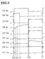
- the first switch control signal Vg 1 applied from the switch control circuit 4 to the first switch Q 1 is shown at (A) in FIG. 3, and the second switch control signal Vg 2 applied therefrom to the second switch Q 2 at (B) in FIG. 3.
- the switch control circuit 4 has a voltage detector circuit 11 connected to the pair of converter output terminals 2 a and 2 b for putting out a signal indicative of the converter output voltage.
- This detector output signal is applied to one input of a differential amplifier 12, the other input of which is connected to a source 13 of a reference voltage representative of a target value at which the converter output voltage should be maintained.
- the output V 1 from the differential amplifier 12, indicative of a possible departure of the converter output voltage from the target value is applied to one input of a comparator 15, the other input of which is connected to a wave generator 14.
- the wave generator 14 generates a triangular wave or a sawtooth as a periodic wave having a high frequency (e.g. 20-150 kHz).
- FIG. 4 shows at (A) both the departure signal V 1 and the triangular wave voltage Vt of, say, 20-150 kHz delivered from the wave generator 14 to the comparator 15.
- the resulting output from the comparator 15 is a series of duration-modulated pulses indicated at (B) in FIG. 4, which are impressed as the noted first switch control signal Vg 1 , (A) in FIG. 3, to the first switch Q 1 .
- a voltage divider circuit 16 having two resistors R 1 and R 2 connected in series between differential amplifier output and ground.
- the output V 2 from the voltage divider circuit 16, with a voltage less than that of the departure signal V 1 is delivered to one input of a second comparator 17, the other input of which receives the triangular wave voltage Vt from the wave generator 14.
- the resulting output from the second comparator 17 is another series of duration-modulated pulses seen at (C) in FIG. 4, which are delivered to a monostable multivibrator (MMV) 18.
- MMV monostable multivibrator
- the MMV 18 will put out the pulses shown at (D) in FIG. 4.
- These MMV output pulses constitute the second switch control signal Vg 2 , (B) in FIG. 3, each lasting as from a first moment t 0 to a second moment t 4 .
- the moment t 4 of decay of each pulse of the second switch control signal Vg 2 may be delayed until t 5 at a maximum.
- the second switch control signal Vg 2 is delivered to the second switch Q 2 .
- FIGS. 1 and 2 flyback d.c.-to-d.c. converter will be best understood by separately studying what happens in the before- t 0 period, t 0 - t 1 period, t 1 - t 2 period, t 2 - t 3 period, t 3 - t 4 period, t 4 - t 5 period, t 5 - t 6 , and t 6 - t 7 period of FIG. 3.
- the following operational description will therefore be divided under the subheadings denoting these periods.
- the switches Q 1 and Q 2 are both open during these periods. As the energy that has been stored on the transformer T during the previous conducting period of the first switch Q 1 is released, there will build up across the transformer secondary N 2 a voltage that will forward-bias the rectifying diode Do. With the consequent conduction of the rectifying diode Do as at (G) in FIG. 3, the smoothing capacitor Co will be charged, and the load Ro powered.
- the second switch Q 2 is turned on at t 0 , and the first switch Q 1 at t 1 , as at (A) and (B) in FIG. 3.
- the resonant capacitor C 1 will be discharged by resonance during this period, resulting in a gradual drop of the voltage Vq 1 , (C) in FIG. 3, across the first switch Q 1 to zero.
- the second switch Q 2 Since the second switch Q 2 is conductive throughout the t 0 - t 1 period, a current will flow both along a first path comprising the power supply Ei , transformer tertiary N 3 , transformer quaternary N 4 , resonant inductor L 1 , third diode D 3 , and second switch Q 2 , and a second path comprising the resonant capacitor C 1 , transformer primary N 1 , transformer tertiary N 3 , transformer quaternary N 4 , resonant inductor L 1 , third diode D 3 , and second switch Q 2 .
- the voltage Vq 1 across the first switch Q 1 is practically zero when the first switch is turned on at t 1 .
- This zero-voltage switching of the first switch Q 1 leads to the reduction of switching loss.
- a current will flow through the path comprising the resonant inductor L 1 , third diode D 3 , second switch Q 2 , first diode D 1 or first switch Q 1 , transformer primary N 1 , transformer tertiary N 3 , and transformer quaternary N 4 .
- a current will also flow through the path comprising the resonant inductor L 1 , third diode D 3 , second switch Q 2 , power supply Ei , transformer tertiary N 3 , and transformer quaternary N 4 , as well as through the path comprising the resonant inductor L 1 , third diode D 3 , second switch Q 2 , fourth diode D 4 , and transformer quaternary N 4 .
- the current Iq 1 shown at (D) in FIG. 3 represents the sum of the current through the first switch Q 1 and the current through the first diode D 1 .
- the current Iq 1 is therefore negative when the current is flowing through the first diode D 1 .
- the residual energy of the resonant inductor L 1 will therefore be released through the path comprising the resonant inductor L 1 , third diode D 3 , second switch Q 2 , power supply Ei , transformer tertiary N 3 , and transformer quaternary N 4 during this t 2 - t 3 period.
- the forward current Iq 1 of the first switch will flow through the path comprising the power supply Ei , transformer primary N 1 , and first switch Q 1 .
- the rectifying diode Do is now nonconductive, so that energy will be stored on the inductive transformer T.
- the conducting period of the second switch Q 2 should expire at or after t 3 and at latest t 5 . Further the starting moment t 0 of the t 0 - t 4 conducting period of the second switch Q 2 should be so determined that the voltage Vq 1 across the first switch Q 1 may be made approximately zero by resonance at the subsequent starting moment t 1 of the conducting period of the first switch. In short the t 0 -t 1 period should be sufficiently long for the resonant capacitor C 1 to be substantially fully discharged. The length of time required for the voltage Vq 1 across the first switch Q 1 to change from its value at t 0 to that at t 1 depends upon the circuit constant of the resonant circuit.
- the voltage divider circuit 16, FIG. 2, of the switch control circuit 4 is designed to determine one of the input levels of the second comparator 17 in order that the t 0 - t 1 period of FIG. 3 may be obtained.
- the first switch Q 1 may be turned on at any moment from t 1 , when the voltage Vq 1 across the first switch becomes zero as at (C) in FIG. 3, to t 2 when the first diode D 1 becomes nonconductive.
- the voltage across the first switch Q 1 is zero during the t 1 - t 2 period when the voltage across the resonant capacitor C 1 is zero and when the first diode D 1 is conductive.
- the first switch Q 1 can therefore be zero-voltage switched by the first switch control signal Vg 1 , (A) in FIG. 3, during the t 1 - t 2 period.
- the first switch control signal Vg 1 to go high at t 1 .
- the first switch control signal Vg 1 may go high preferably at a moment approximately midway between t 1 and t 2 .
- the switching loss will be reduced by an amount proportional to the drop of the first switch voltage Vq 1 .
- the first switch Q 1 may be turned on at any moment that is later than t 0 , when the second switch Q 2 is turned on, as long as the voltage Vq 1 across the first switch Q 1 is less than that when the first switch is off.
- the second switch Q 2 is turned off at t 4 which is later than t 3 when the current Iq 2 through the second switch becomes zero as at (F) in FIG. 3. Zero-current turnoff of the second switch Q 2 is thus accomplished for less power loss due to the second switch.
- the current Iq 1 will flow through the path comprising the power supply Ei , transformer primary Ni , and first switch Q 1 , causing energy to be stored on the transformer T.
- the current through the transformer primary N 1 which is inductive, will increase in magnitude with time, as at (D) in FIG. 3.
- the rectifying diode Do is nonconductive during this period, so that power will be fed to the load Ro from the smoothing capacitor Co.
- This brief period is a period of transition from the conductive to the nonconductive state of the first switch Q 1 .
- the resonant capacitor C 1 will start to be charged when the first switch Q 1 is actually turned off in response to the going-low of the first switch control signal Vg 1 , (A) in FIG. 3 , at t 5 .
- the voltage Vg 1 across the resonant capacitor C 1 and hence across the first switch Q 1 will build up, as at (C) in FIG. 3, in step with the progress of the charging of the capacitor. It is thus seen that the zero-voltage turning-off of the first switch Q 1 has been accomplished.
- the energy that has been stored on the transformer T will start to be released in this period, and the diode current Ido will start flowing as at (G) in FIG. 3.
- the t 6 - t 7 period of FIG. 3 is akin to the pre- t 0 period set forth above.
- One cycle of converter operation, which has started at t 0 comes to an end at t 7 , and the same cycle repeats itself thereafter.
- the durations of the output pulses Vg 1 and Vg 2 , (A) and (B) in FIG. 3, of the two comparators 15 and 17 of the switch control circuit 4 are subject to change depending upon the magnitude of the converter output voltage. For instance, upon increase in the converter output voltage above the target value, both the output voltage V 1 of the differential amplifier 12 and the output voltage V 2 of the voltage divider circuit 16 will become proportionately higher.
- a study of FIG. 4 will show that, inputting these higher voltages, the comparators 15 and 17 put out pulses of correspondingly shorter durations.
- the shorter-duration output pulses of the first comparator 15 will lessen the duty ratio of the first switch Q 1 , with the result that less power will be fed from transformer T to load Ro. It is self-evident, then, how more power is fed to the load Ro in the event of a drop in the converter output voltage below the target value.
- FIG. 5 shows a modified switch control circuit 4 a for use in the FIG. 1 d.c.-to-d.c. converter in substitution for the FIG. 2 switch control circuit 4.
- FIGS. 2 and 5 show that the switch control circuits 4 and 4 a are alike in having the comparators 15 and 17 and all the means connected to their inputs.
- the inputs to, and outputs from, the comparators 15 and 17 of the modified switch control circuit 4 a are as depicted at (A)-(C) in FIG. 6, which are equivalent to (A)-(C) in FIG. 4.
- the output stages of the FIG. 5 comparators 15 and 17 differ from those of their FIG. 2 counterparts.
- the output of the first comparator 15 is connected to both pulse rise detector circuit 21 and pulse decay detector circuit 22, and the output of the second comparator 17 to both pulse rise detector circuit 23 and pulse decay detector circuit 24.
- the pulse rise detector circuits 21 and 23 are connected to the set inputs S of RS flip-flops 25 and 26, respectively.
- the first pulse decay detector circuit 22 is connected to the reset input R of the second flip-flop 26, and the second pulse decay detector circuit 24 to the reset input R of the first flip-flop 25.
- the noninverting outputs Q of the flip-flops 25 and 26 are connected to the gates of the FET switches Q 1 and Q 2 , respectively, of the FIG. 1 d.c.-to-d.c. converter.
- the first pulse rise detector circuit 21 puts out a series of trigger pulses P 1 , (C) in FIG. 6, in response to the leading edges of the FIG. 6 (B) output pulses of the first comparator 15.
- the first pulse decay detector circuit 23 puts out a series of trigger pulses P 2 , FIG. 6 (E), in response to the trailing edges of the FIG. 6 (B) output pulses of the first comparator 15.
- the second pulse rise detector circuit 23 puts out a series of trigger pulses P 3 , FIG. 6 (F), in response to the leading edges of the FIG. 6 (C) output pulses of the second comparator 17.
- the second pulse decay detector circuit 24 responds to the trailing edges of the FIG. 6 (C) output pulses of the second comparator 17 by producing a series of trigger pulses P 4 , FIG. 6 (G).
- the first flip-flop 25 will therefore be set, as at t 1 in FIG. 6, by each output pulse P 1 of the first pulse rise detector circuit 21, and reset, as at t 5 , by each output pulse P 4 of the second pulse decay detector circuit 24. So set and reset, the first flip-flop 25 will provide the first switch control signal Vg 1 , FIG. 6 (H), consisting of a series of pulses each lasting as from t 1 to t 5 in FIG. 6, for delivery to the first switch Q 1 , FIG. 1.
- the second flip-flop 26 will be set, as at t 0 in FIG. 6, by each output pulse P 3 of the second pulse ride detector circuit 23, and reset, as at t 4 , by each output pulse P 2 of the first pulse decay detector circuit 22.
- the second flip-flop 26 will thus provide the second switch control signal Vg 2 , FIG. 6 (I), consisting of a series of pulses each lasting as from t 0 to t 4 in FIG. 6.
- switch control circuit 4 a An advantage peculiar to the FIG. 5 switch control circuit 4 a is that the durations of both first and second series of switch control pulses Vg 1 and Vg 2 are correlated. The durations of the first series of switch control pulses Vg 1 may therefore be determined at will without regard to the durations of the second series of switch control pulses Vg 2 .
Landscapes
- Engineering & Computer Science (AREA)
- Power Engineering (AREA)
- Dc-Dc Converters (AREA)
Abstract
Description
Claims (8)
- A d.c.-to-d.c. converter comprising a pair of input terminals (1a, 1b) to be connected to a d.c. power supply (Ei), a pair of output terminals (2a, 2b) to be connected to a load (Ro), a transformer (T) having a primary winding (N 1) and a secondary winding (N 2), said primary winding having one extremity thereof connected to one (1a) of said pair of input terminals, a rectifying and smoothing circuit (3) connected between said secondary winding of said transformer and said pair of output terminals, and a first switch (Q 1) connected between the other extremity of said primary winding of said transformer and the other (1b) of said pair of input terminals, characterized in that said transformer (T) has a tertiary winding (N 3) and a quaternary winding (N 4) which are electromagnetically coupled with said primary winding (N 1) and said secondary winding (N 2), that said tertiary and quaternary windings of said transformer and resonant inductance means (L 1) and a first diode (D 3) and a second switch (Q 2) are all connected in series with one another and in parallel with the serial connection of said primary winding of said transformer and said first switch, said first diode being so oriented as to be forward-biased by a supply voltage to be applied from said pair of input terminals, that a second diode (D 4) is connected in parallel with the serial connection of said quaternary winding of said transformer and said resonant inductance means and said first diode and said second switch, said second diode being so oriented as to be reverse-biased by the supply voltage to be applied from said pair of input terminals, and a switch control circuit (4 or 4a) is connected to said first and said second switch (Q 1, Q 2) for making on-off control of said first and said second switch, said switch control circuit including means for turning on said second switch at any moment between a first moment (t 0) that is earlier than a starting moment (t 1) of each conducting period of said first switch and a second moment that is equal to or earlier than an ending moment (t 5) of each conducting period of said first switch.
- The d.c.-to-d.c. converter as claimed in claim 1, characterized in that said switch control circuit (4) comprises voltage detector means (11, 12) connected to said rectifying and smoothing circuit (3) for putting out a voltage (V 1) in proportion to the converter output voltage being applied to the load, a voltage divider circuit (16) connected to said voltage detector means for putting out a voltage (V 2) indicative of a predetermined fraction of the output voltage of said voltage detector means, a wave generator (14) for generating a periodic wave (Vt), a first comparator (15) having inputs connected to said voltage detector means and said wave generator (14) for putting out a first switch control signal (Vg 1) in the form of a series of pulses indicative of whether the output voltage of said voltage detector means is greater or less than the periodic wave (Vt), said first comparator having an output connected to said first switch (Q 1) for on-off control thereof by the first switch control signal, a second comparator (17) having inputs connected to said voltage divider circuit and said wave generator (14) for providing a series of output pulses indicative of whether the output voltage of said voltage divider circuit is greater or less than the periodic wave (Vt), and a pulse generator (18) connected to said second comparator for putting out a second switch control signal (Vg 2) in the form of a series of pulses each rising with one output pulse of said second comparator and each decaying equal to or earlier than one output pulse of said first comparator, said pulse generator having an output connected to said second switch (Q 2) for on-off control thereof by the second switch control signal.
- The d.c.-to-d.c. converter as claimed in claim 2, characterized in that said pulse generator (18) of said switch control circuit (4) is a monostable multivibrator.
- The d.c.-to-d.c. converter as claimed in claim 1, characterized in that said switch control circuit (4a) comprises voltage detector means (11, 12) connected to said rectifying and smoothing circuit (3) for putting out a voltage (V 1) in proportion to the converter output voltage being applied to the load, a voltage divider circuit (16) connected to said voltage detector means for putting out a voltage (V 2) indicative of a predetermined fraction of the output voltage of said voltage detector means, a wave generator (14) for generating a periodic wave (Vt), a first comparator (15) having inputs connected to said voltage detector means and said wave generator (14) for putting out a first series of pulses indicative of whether the output voltage of said voltage detector means is greater or less than the periodic wave (Vt), a second comparator (17) having inputs connected to said voltage divider circuit and said wave generator (14) for putting out a second series of pulses indicative of whether the output voltage of said voltage divider circuit is greater or less than the periodic wave (Vt), a first pulse rise detector circuit (22) connected to said first comparator for detecting the rise of each output pulse thereof, a first pulse decay detector circuit (22) connected to said first comparator for detecting the decay of each output pulse thereof, a second pulse rise detector circuit (23) connected to said second comparator for detecting the rise of each output pulse thereof, a second pulse decay detector circuit (24) connected to said second comparator for detecting the decay of each output pulse thereof, a first flip-flop (25) connected to said first pulse rise detector circuit and said second pulse decay detector circuit in order to be set in response to the leading edge of each output pulse of said first comparator and reset in response to the trailing edge of each output pulse of said second comparator, said first flip-flop putting out a first switch control signal (Vg 1) for on-off control of said first switch (Q 1), and a second flip-flop (26) connected to said second pulse rise detector circuit and said first pulse decay detector circuit in order to be set in response to the leading edge of each output pulse of said second comparator and reset in response to the trailing edge of each output pulse of said first comparator, said second flip-flop putting out a second switch control signal (Vg 2) for on-off control of said second switch (Q 2).
- The d.c.-to-d.c. converter as claimed in claim 1, characterized in that said rectifying and smoothing circuit (3) comprises a rectifying diode (Do) connected to one extremity of said secondary winding (N 2) of said transformer (T) and so polarized as to become conductive in response to a voltage building up in said transformer secondary when said first switch (Q 2) is off, and a smoothing capacitor (Co) connected in parallel with said transformer secondary via said rectifying diode.
- The d.c.-to-d.c. converter as claimed in claim 1, characterized in that said tertiary winding (N 3) and quaternary winding (N 4) of said transformer (T) are of the same polarity as said primary winding (N 1) of said transformer with respect to the supply voltage to be applied from said pair of input terminals (1a, 1b).
- The d.c.-to-d.c. converter as claimed in claim 1, characterized in that a resonant capacitor (C 1) is connected in parallel with said first switch (Q 1).
- The d.c.-to-d.c. converter as claimed in claim 1, characterized in that a third diode (D 1) is connected in parallel with said first switch, said third diode being so oriented as to be reverse-biased by the supply voltage to be applied from said pair of input terminals.
Applications Claiming Priority (2)
| Application Number | Priority Date | Filing Date | Title |
|---|---|---|---|
| JP2000162455 | 2000-05-31 | ||
| JP2000162455 | 2000-05-31 |
Publications (2)
| Publication Number | Publication Date |
|---|---|
| EP1160963A2 true EP1160963A2 (en) | 2001-12-05 |
| EP1160963A3 EP1160963A3 (en) | 2004-02-04 |
Family
ID=18666348
Family Applications (1)
| Application Number | Title | Priority Date | Filing Date |
|---|---|---|---|
| EP01111877A Withdrawn EP1160963A3 (en) | 2000-05-31 | 2001-05-16 | DC-to-DC converter |
Country Status (4)
| Country | Link |
|---|---|
| US (1) | US6396719B2 (en) |
| EP (1) | EP1160963A3 (en) |
| KR (1) | KR100403209B1 (en) |
| CN (1) | CN1168194C (en) |
Cited By (2)
| Publication number | Priority date | Publication date | Assignee | Title |
|---|---|---|---|---|
| CN101494419B (en) * | 2008-01-21 | 2011-05-18 | 许继集团有限公司 | High efficiency zero voltage, zero current whole bridge converter |
| CN105119391A (en) * | 2015-09-27 | 2015-12-02 | 宁波微鹅电子科技有限公司 | High-efficiency electric energy transmitting terminal and wireless electric energy transmission apparatus |
Families Citing this family (18)
| Publication number | Priority date | Publication date | Assignee | Title |
|---|---|---|---|---|
| JP3475943B2 (en) * | 2001-06-29 | 2003-12-10 | サンケン電気株式会社 | Switching power supply |
| JP4151014B2 (en) * | 2003-03-11 | 2008-09-17 | 株式会社デンソー | Isolated switching DC / DC converter |
| US7057906B2 (en) * | 2003-03-11 | 2006-06-06 | Denso Corporation | Insulating switching DC/DC converter |
| AT413910B (en) * | 2003-08-06 | 2006-07-15 | Siemens Ag Oesterreich | POWER SUPPLY |
| JP3882809B2 (en) * | 2003-11-26 | 2007-02-21 | サンケン電気株式会社 | Switching power supply |
| JP3861871B2 (en) * | 2003-11-26 | 2006-12-27 | サンケン電気株式会社 | Switching power supply |
| DE102004013108B4 (en) * | 2004-03-17 | 2011-03-10 | Beckhoff Automation Gmbh | Method for operating a supply unit for a driver circuit and supply unit for a driver circuit |
| US7174260B2 (en) * | 2004-04-01 | 2007-02-06 | Blue Line Innovations Inc. | System and method for reading power meters |
| JP3829142B2 (en) * | 2004-10-29 | 2006-10-04 | Tdk株式会社 | Discharge lamp driving device |
| JP4347249B2 (en) * | 2005-03-31 | 2009-10-21 | 富士通マイクロエレクトロニクス株式会社 | DC-DC converter, control circuit for DC-DC converter, and control method for DC-DC converter |
| US20060267561A1 (en) * | 2005-05-27 | 2006-11-30 | Cherokee International Corporation | Power factor correction circuit for DC-DC converters with low resonance current |
| FR2887704B1 (en) * | 2005-06-27 | 2007-08-10 | Agence Spatiale Europeenne | VOLTAGE REGULATOR CONVERTER WITHOUT SWITCHING LOSSES |
| US8360904B2 (en) | 2007-08-17 | 2013-01-29 | Adidas International Marketing Bv | Sports electronic training system with sport ball, and applications thereof |
| JP5854895B2 (en) * | 2011-05-02 | 2016-02-09 | 三菱電機株式会社 | Power semiconductor device |
| US9407154B2 (en) * | 2013-06-14 | 2016-08-02 | Advanced Charging Technologies, LLC | Electrical circuit for delivering power to consumer electronic devices |
| DE112016007515B4 (en) * | 2016-12-12 | 2024-07-18 | Mitsubishi Electric Corporation | Drive method and drive circuit for semiconductor device |
| US10342084B1 (en) * | 2018-10-02 | 2019-07-02 | New Energies & Alternative Technologies, Inc. | Oscillating driver circuits |
| CN114079385B (en) * | 2021-11-23 | 2023-07-28 | 吕真 | LLC resonant circuit series-parallel conversion power supply circuit based on synchronous drive |
Family Cites Families (7)
| Publication number | Priority date | Publication date | Assignee | Title |
|---|---|---|---|---|
| US4559590A (en) * | 1983-03-24 | 1985-12-17 | Varian Associates, Inc. | Regulated DC to DC converter |
| JPS62166777A (en) * | 1986-01-16 | 1987-07-23 | Sanken Electric Co Ltd | Dc-dc converter |
| JP3450929B2 (en) * | 1995-03-23 | 2003-09-29 | 株式会社リコー | Switching power supply |
| JP2845188B2 (en) * | 1995-12-11 | 1999-01-13 | サンケン電気株式会社 | DC-DC converter |
| DE19855615A1 (en) * | 1997-12-03 | 1999-06-10 | Fuji Electric Co Ltd | Switched network supply device |
| JP2991181B2 (en) * | 1998-02-27 | 1999-12-20 | 富士電機株式会社 | Switching power supply |
| JP2956681B2 (en) * | 1998-02-27 | 1999-10-04 | 富士電機株式会社 | Switching operation circuit of switching power supply |
-
2001
- 2001-05-16 EP EP01111877A patent/EP1160963A3/en not_active Withdrawn
- 2001-05-17 US US09/859,935 patent/US6396719B2/en not_active Expired - Fee Related
- 2001-05-31 KR KR10-2001-0030335A patent/KR100403209B1/en not_active Expired - Fee Related
- 2001-05-31 CN CNB011194677A patent/CN1168194C/en not_active Expired - Fee Related
Cited By (3)
| Publication number | Priority date | Publication date | Assignee | Title |
|---|---|---|---|---|
| CN101494419B (en) * | 2008-01-21 | 2011-05-18 | 许继集团有限公司 | High efficiency zero voltage, zero current whole bridge converter |
| CN105119391A (en) * | 2015-09-27 | 2015-12-02 | 宁波微鹅电子科技有限公司 | High-efficiency electric energy transmitting terminal and wireless electric energy transmission apparatus |
| CN105119391B (en) * | 2015-09-27 | 2019-01-01 | 宁波微鹅电子科技有限公司 | A kind of efficient electric energy transmitting terminal and wireless electric energy transmission device |
Also Published As
| Publication number | Publication date |
|---|---|
| KR100403209B1 (en) | 2003-10-23 |
| CN1168194C (en) | 2004-09-22 |
| CN1329389A (en) | 2002-01-02 |
| US20010050853A1 (en) | 2001-12-13 |
| US6396719B2 (en) | 2002-05-28 |
| EP1160963A3 (en) | 2004-02-04 |
| KR20010109197A (en) | 2001-12-08 |
Similar Documents
| Publication | Publication Date | Title |
|---|---|---|
| US6396719B2 (en) | Dc-to-dc converter | |
| US5729444A (en) | High-efficiency DC-DC converter | |
| US6373727B1 (en) | Synchronous rectification in a flyback converter | |
| US9252676B2 (en) | Adaptive active clamp of flyback power converter with high efficiency for heavy load and light load | |
| US6788556B2 (en) | Switching power source device | |
| US7869235B2 (en) | Flyback converter having an active snubber | |
| US6320763B2 (en) | Switching power supply unit | |
| US6466462B2 (en) | DC/DC converter having a control circuit to reduce losses at light loads | |
| CN101257257B (en) | Off-line synchronous switching regulator | |
| US7426120B2 (en) | Switching control circuit having a valley voltage detector to achieve soft switching for a resonant power converter | |
| EP1037368B1 (en) | Isolating DC-DC converter | |
| WO2000069057A1 (en) | Single-ended forward converter circuit with quasi-optimal resetting for synchronous rectification | |
| JPH09163736A (en) | Dc-dc converter | |
| EP0767528B1 (en) | Tuned switch-mode power supply with current mode control | |
| EP0936726A2 (en) | Schaltnetzteil mit Schwellwertschaltung | |
| JPH06276078A (en) | Switch circuit | |
| JP2001333576A (en) | Control method of DC / DC converter | |
| JP2002044946A (en) | Switching power unit | |
| JP2003143835A (en) | Dc-dc conversion circuit and pulse signal interval setting circuit | |
| JP4484006B2 (en) | Switching power supply | |
| JP3000937B2 (en) | Switching power supply | |
| JP3334754B2 (en) | Switching power supply | |
| JP3409851B2 (en) | DC-DC converter | |
| JP7622899B2 (en) | Active Clamp Flyback Converter | |
| JP3371960B2 (en) | DC-DC converter |
Legal Events
| Date | Code | Title | Description |
|---|---|---|---|
| PUAI | Public reference made under article 153(3) epc to a published international application that has entered the european phase |
Free format text: ORIGINAL CODE: 0009012 |
|
| AK | Designated contracting states |
Kind code of ref document: A2 Designated state(s): AT BE CH CY DE DK ES FI FR GB GR IE IT LI LU MC NL PT SE TR |
|
| AX | Request for extension of the european patent |
Free format text: AL;LT;LV;MK;RO;SI |
|
| PUAL | Search report despatched |
Free format text: ORIGINAL CODE: 0009013 |
|
| AK | Designated contracting states |
Kind code of ref document: A3 Designated state(s): AT BE CH CY DE DK ES FI FR GB GR IE IT LI LU MC NL PT SE TR |
|
| AX | Request for extension of the european patent |
Extension state: AL LT LV MK RO SI |
|
| 17P | Request for examination filed |
Effective date: 20040415 |
|
| AKX | Designation fees paid |
Designated state(s): DE FR GB |
|
| STAA | Information on the status of an ep patent application or granted ep patent |
Free format text: STATUS: THE APPLICATION IS DEEMED TO BE WITHDRAWN |
|
| 18D | Application deemed to be withdrawn |
Effective date: 20051201 |