EP1160864A2 - Semiconductor device with a corrosion resistant bonding pad and manufacturing method thereof - Google Patents
Semiconductor device with a corrosion resistant bonding pad and manufacturing method thereof Download PDFInfo
- Publication number
- EP1160864A2 EP1160864A2 EP01110760A EP01110760A EP1160864A2 EP 1160864 A2 EP1160864 A2 EP 1160864A2 EP 01110760 A EP01110760 A EP 01110760A EP 01110760 A EP01110760 A EP 01110760A EP 1160864 A2 EP1160864 A2 EP 1160864A2
- Authority
- EP
- European Patent Office
- Prior art keywords
- bonding pad
- semiconductor device
- bonding
- wiring layer
- layer
- Prior art date
- Legal status (The legal status is an assumption and is not a legal conclusion. Google has not performed a legal analysis and makes no representation as to the accuracy of the status listed.)
- Withdrawn
Links
Images



Classifications
-
- H—ELECTRICITY
- H10—SEMICONDUCTOR DEVICES; ELECTRIC SOLID-STATE DEVICES NOT OTHERWISE PROVIDED FOR
- H10W—GENERIC PACKAGES, INTERCONNECTIONS, CONNECTORS OR OTHER CONSTRUCTIONAL DETAILS OF DEVICES COVERED BY CLASS H10
- H10W72/00—Interconnections or connectors in packages
- H10W72/071—Connecting or disconnecting
-
- H—ELECTRICITY
- H10—SEMICONDUCTOR DEVICES; ELECTRIC SOLID-STATE DEVICES NOT OTHERWISE PROVIDED FOR
- H10W—GENERIC PACKAGES, INTERCONNECTIONS, CONNECTORS OR OTHER CONSTRUCTIONAL DETAILS OF DEVICES COVERED BY CLASS H10
- H10W72/00—Interconnections or connectors in packages
- H10W72/01—Manufacture or treatment
- H10W72/019—Manufacture or treatment of bond pads
-
- H—ELECTRICITY
- H10—SEMICONDUCTOR DEVICES; ELECTRIC SOLID-STATE DEVICES NOT OTHERWISE PROVIDED FOR
- H10W—GENERIC PACKAGES, INTERCONNECTIONS, CONNECTORS OR OTHER CONSTRUCTIONAL DETAILS OF DEVICES COVERED BY CLASS H10
- H10W72/00—Interconnections or connectors in packages
- H10W72/071—Connecting or disconnecting
- H10W72/075—Connecting or disconnecting of bond wires
-
- H—ELECTRICITY
- H10—SEMICONDUCTOR DEVICES; ELECTRIC SOLID-STATE DEVICES NOT OTHERWISE PROVIDED FOR
- H10W—GENERIC PACKAGES, INTERCONNECTIONS, CONNECTORS OR OTHER CONSTRUCTIONAL DETAILS OF DEVICES COVERED BY CLASS H10
- H10W72/00—Interconnections or connectors in packages
- H10W72/071—Connecting or disconnecting
- H10W72/075—Connecting or disconnecting of bond wires
- H10W72/07531—Techniques
- H10W72/07532—Compression bonding, e.g. thermocompression bonding
- H10W72/07533—Ultrasonic bonding, e.g. thermosonic bonding
-
- H—ELECTRICITY
- H10—SEMICONDUCTOR DEVICES; ELECTRIC SOLID-STATE DEVICES NOT OTHERWISE PROVIDED FOR
- H10W—GENERIC PACKAGES, INTERCONNECTIONS, CONNECTORS OR OTHER CONSTRUCTIONAL DETAILS OF DEVICES COVERED BY CLASS H10
- H10W72/00—Interconnections or connectors in packages
- H10W72/50—Bond wires
- H10W72/531—Shapes of wire connectors
- H10W72/5363—Shapes of wire connectors the connected ends being wedge-shaped
-
- H—ELECTRICITY
- H10—SEMICONDUCTOR DEVICES; ELECTRIC SOLID-STATE DEVICES NOT OTHERWISE PROVIDED FOR
- H10W—GENERIC PACKAGES, INTERCONNECTIONS, CONNECTORS OR OTHER CONSTRUCTIONAL DETAILS OF DEVICES COVERED BY CLASS H10
- H10W72/00—Interconnections or connectors in packages
- H10W72/50—Bond wires
- H10W72/551—Materials of bond wires
- H10W72/552—Materials of bond wires comprising metals or metalloids, e.g. silver
- H10W72/5522—Materials of bond wires comprising metals or metalloids, e.g. silver comprising gold [Au]
-
- H—ELECTRICITY
- H10—SEMICONDUCTOR DEVICES; ELECTRIC SOLID-STATE DEVICES NOT OTHERWISE PROVIDED FOR
- H10W—GENERIC PACKAGES, INTERCONNECTIONS, CONNECTORS OR OTHER CONSTRUCTIONAL DETAILS OF DEVICES COVERED BY CLASS H10
- H10W72/00—Interconnections or connectors in packages
- H10W72/50—Bond wires
- H10W72/551—Materials of bond wires
- H10W72/552—Materials of bond wires comprising metals or metalloids, e.g. silver
- H10W72/5524—Materials of bond wires comprising metals or metalloids, e.g. silver comprising aluminium [Al]
-
- H—ELECTRICITY
- H10—SEMICONDUCTOR DEVICES; ELECTRIC SOLID-STATE DEVICES NOT OTHERWISE PROVIDED FOR
- H10W—GENERIC PACKAGES, INTERCONNECTIONS, CONNECTORS OR OTHER CONSTRUCTIONAL DETAILS OF DEVICES COVERED BY CLASS H10
- H10W72/00—Interconnections or connectors in packages
- H10W72/50—Bond wires
- H10W72/59—Bond pads specially adapted therefor
-
- H—ELECTRICITY
- H10—SEMICONDUCTOR DEVICES; ELECTRIC SOLID-STATE DEVICES NOT OTHERWISE PROVIDED FOR
- H10W—GENERIC PACKAGES, INTERCONNECTIONS, CONNECTORS OR OTHER CONSTRUCTIONAL DETAILS OF DEVICES COVERED BY CLASS H10
- H10W72/00—Interconnections or connectors in packages
- H10W72/90—Bond pads, in general
- H10W72/921—Structures or relative sizes of bond pads
- H10W72/923—Bond pads having multiple stacked layers
-
- H—ELECTRICITY
- H10—SEMICONDUCTOR DEVICES; ELECTRIC SOLID-STATE DEVICES NOT OTHERWISE PROVIDED FOR
- H10W—GENERIC PACKAGES, INTERCONNECTIONS, CONNECTORS OR OTHER CONSTRUCTIONAL DETAILS OF DEVICES COVERED BY CLASS H10
- H10W72/00—Interconnections or connectors in packages
- H10W72/90—Bond pads, in general
- H10W72/951—Materials of bond pads
- H10W72/952—Materials of bond pads comprising metals or metalloids, e.g. PbSn, Ag or Cu
-
- H—ELECTRICITY
- H10—SEMICONDUCTOR DEVICES; ELECTRIC SOLID-STATE DEVICES NOT OTHERWISE PROVIDED FOR
- H10W—GENERIC PACKAGES, INTERCONNECTIONS, CONNECTORS OR OTHER CONSTRUCTIONAL DETAILS OF DEVICES COVERED BY CLASS H10
- H10W72/00—Interconnections or connectors in packages
- H10W72/90—Bond pads, in general
- H10W72/981—Auxiliary members, e.g. spacers
- H10W72/983—Reinforcing structures, e.g. collars
-
- H—ELECTRICITY
- H10—SEMICONDUCTOR DEVICES; ELECTRIC SOLID-STATE DEVICES NOT OTHERWISE PROVIDED FOR
- H10W—GENERIC PACKAGES, INTERCONNECTIONS, CONNECTORS OR OTHER CONSTRUCTIONAL DETAILS OF DEVICES COVERED BY CLASS H10
- H10W74/00—Encapsulations, e.g. protective coatings
Definitions
- the present invention relates to a semiconductor device, and more particularly to a semiconductor device in which reaction products such as aluminum hydroxide are prevented from forming on a bonding pad, and a method of manufacturing such a device.
- Aluminum Materials with aluminum as the main constituent, for example Al, Al-Cu, and Al-Si-Cu, have been used for metal wiring in semiconductor devices. Bonding pads are formed by selectively exposing such metal wiring. When openings are formed for bonding pads, the metal wiring exposed by the openings reacts with moisture in the air at room temperature. The aluminum in the wiring is thereby transformed into aluminum hydroxide, since aluminum is a very active element. Aluminum hydroxide can form in about two weeks where temperature and humidity are not controlled.
- an inter-layer insulating film 2, a barrier metal film 3, an aluminum layer 4, an antireflection metal film 5, and a passivation film 6 are formed as a multi-layer structure on a semiconductor substrate 1. Furthermore, a photosensitive polyimide layer (or photoresist) 7 is formed on the passivation film 6, and the passivation film (protective film) 6 is selectively removed by dry etching to form an opening 8 using the polyimide layer 7 as a mask. This opening 8 exposes the aluminum layer 4 as bonding pad 11. If this opening 8 is left as is, an aluminum hydroxide layer 12 will form as a reaction product on the surface of aluminum layer 4.
- Such an aluminum hydroxide layer 12 hinders a eutectic state between aluminum serving as the bonding pad and the bonding wire (Au or Al wire) in the subsequent bonding process, and therefore decreases the bonding yield. Therefore, in the method of manufacturing a semiconductor device, to minimize the degeneration of the surface of the bonding pad, it is common to keep the device in a controlled temperature and humidity, or confined in dry air after the front-end process (the completion of the bonding pad forming step) until the assembly is completed.
- the semiconductor device is completed by bonding the bonding pad to an external lead, such as a lead frame, with a metal wire, and then packaging.
- an external lead such as a lead frame
- packaging is performed with the bonding area exposed to air.
- the surface of the aluminum serving as bonding pad reacts with moisture in the air. Accordingly, the surface of the bonding pad degenerates and erodes, and the characteristics of the semiconductor device degrade.
- Japanese Patent Kokai No. Sho 59-150460, No. Sho 63-272042, No. Hei 1-110749, and No. Hei 5-46978 disclose that after the bonding step, the surface of the bonding pad is covered with an insulating film, such as aluminum oxide, to prevent the aluminum serving as the bonding pad from degenerating.
- an insulating film such as aluminum oxide
- the device in the conventional manufacturing method of a semiconductor device, the device must be kept in a controlled temperature and humidity or confined in dry air until the assembly is completed. Consequently, handling and storage facilities are needed for keeping the device in the proper atmosphere and additional time is required for transporting the device to the storage place.
- the aluminum oxide is formed after the bonding step, and therefore the device must be kept in the above described storage place from the bonding pad forming step (front-end process) until the assembly is completed.
- the object of the present invention is to provide a semiconductor device and a method of manufacturing a semiconductor device that prevents the surface of the bonding pad from degenerating until the assembly is completed.
- a semiconductor device comprises a semiconductor substrate; a wiring layer on the semiconductor substrate; a passivation film on the wiring layer, the passivation film having a hole selectively formed to expose a surface of the wiring layer serving as a bonding pad; and an oxide layer covering all of the wiring layer exposed by the hole.
- a method of manufacturing a semiconductor device comprises the steps of: forming a wiring layer on a semiconductor substrate; forming a passivation film on the wiring layer; selectively forming a hole in the passivation film to expose a surface of the wiring layer; and forming an aluminum oxide film on the exposed surface of the wiring layer before bonding a bonding wire to the exposed surface.
- Figs. 1A and 1B are a perspective view and a cross sectional view of the structure of a device after a bonding pad formed by etching, respectively.
- Fig. 1C is a cross sectional view of the structure of a device after a bonding step.
- Fig. 2 is a flow chart showing the manufacturing method of a semiconductor device in the first embodiment of the present invention.
- Fig. 3 is a diagram showing an analysis of the surface of a bonding pad of a semiconductor device in the first embodiment of the present invention.
- Fig. 4 is a diagram showing an analysis of the surface of a bonding pad of the conventional semiconductor device.
- Fig. 5 is a diagram showing another analysis of the surface of the bonding pad of a semiconductor device in the first embodiment of the present invention.
- Fig. 6 is a diagram showing another analysis of the surface of a bonding pad of the conventional semiconductor device.
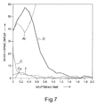
- Fig. 7 is a diagram showing an analysis of the surface of a bonding pad of a semiconductor device in the second embodiment of the present invention.
- Fig. 8 is a cross sectional view of a conventional semiconductor device.
- Fig. 1A is perspective view of a part of the semiconductor device 10 after exposing bonding pads.
- Fig. 1B is a cross-sectional view taken along line A - A' of Fig. 1A.
- an inter-layer insulating film 2 As shown in Fig. 1B, an inter-layer insulating film 2, a barrier metal film 3, a first layer 4 having aluminum as its primary constituent (such as Al, Al-Cu, and Al-Si-Cu), an antireflection metal film 5, and a passivation film 6 are formed as a multi-layer structure on a semiconductor substrate 1.
- a photosensitive polyimide layer (or photoresist) 7 is formed as a mask for an opening 8 on the passivation film 6. The opening 8 is formed to expose a portion of the first layer 4 serving as a bonding pad 11.
- an alumina layer 9 (Al 2 O 3 , aluminum oxide) of 10 to 20nm thickness is formed on the surface of the bonding pad 11 before the bonding step.
- Alumina is chemically very stable, so that alumina protects the surface of the bonding pad and prevents the surface of the bonding pad from degenerating.
- the device is normally kept in controlled temperature and humidity after the front-end process until the assembly is completed because degeneration of the surface of the bonding pad decreases the yield in the bonding step.
- the bonding wire 13 is bonded to the bonding pad 11 by the supersonic wave bonding method.
- the bonding wire 13 pushes the alumina layer 9 with supersonic wave, and the alumina layer 9 is displaced.
- the bonding wire 13 contacts the bonding pad 11, and the bonding wire can be sufficiently alloyed with the bonding pad 11 by heat energy. That is, the bonding wire is sufficiently alloyed with the bonding pad by the general supersonic wave bonding method, if the alumina layer, which is insulation, is 10 to 20 nm thick. Therefore, bonding characteristics are not influenced by the presence of the alumina layer.
- an inter-layer insulating film is formed on the semiconductor substrate (S101) before the formation of the uppermost wiring layer.
- the uppermost wiring layer is patterned on the inter-layer insulating film (S102), and an insulating film is formed on the wiring layer to passivate the wiring layer (S103).
- the wiring layer has aluminum as its main constituent.
- a photosensitive polyimide layer is applied on the insulating film (S104) and photolithography is performed on the photosensitive polyimide layer (S105).
- the semiconductor device including the photosensitive polyimide layer is baked in a nitrogen atmosphere at 380°C for about 1 hour to harden the polyimide (S106).
- Dry etching is performed in a fluorine gas using the polyimide layer as a mask (S107). After dry etching, an O 2 plasma process is performed and the device is soaked in an alkaline solution (S108, S109) in order to remove reaction products of the dry etching. Next, as necessary, the device is baked in nitrogen atmosphere at about 150°C for approximately 60 minutes (S109). The manufacturing method up to this point is the same as the general method of manufacturing a semiconductor device.
- the device is baked in a steam atmosphere (S110) at 200°C to 380°C for 30 minutes or more, for example at 250°C for 30 minutes to form the alumina layer.
- the bonding pad is exposed by selectively removing a passivation film, which is formed on the wiring layer containing aluminum, by dry etching using a photosensitive polyimide film or a photo resist as a mask. If the exposed bonding pad is left as is, aluminum hydroxide will be formed which will cause the problem described before.
- baking the semiconductor device for 30 minutes or more at 200°C to 380°C in water vapor atmosphere forms a good quality alumina (Al 2 O 3 , aluminum oxide) layer on the surface of the bonding pad. That is, an aluminum hydroxide layer 12 is not formed on the surface of the bonding pad.
- the semiconductor wafer is diced into chips (S111), the separated chip is adhered to a lead frame (S112), the bonding pad in a semiconductor device is bonded and connected to the lead frame with an Au wire and the like by the supersonic wave bonding method and the like (S113), and then is further sealed by a mold resin and the like (S114).
- the alumina layer can be formed by processing in oxygen plasma or baking in an atmosphere containing only oxygen after the dry etching.
- baking in a steam atmosphere is superior to these methods for forming a good quality alumina, because aluminum fluoride (AlF 3 ) is formed on the surface of the bonding pad by the fluorine ions in the dry etching gas.
- AlF 3 aluminum fluoride
- the bonding between aluminum and fluoride is not broken by the processing in oxygen plasma or baking in an atmosphere where only oxygen is introduced into the N 2 , so that the good quality alumina cannot be formed.
- aluminum fluoride has a chemical characteristic that it is reduced when heated with hydrogen (H 2 ).
- H 2 hydrogen
- alumina Al 2 O 3
- HF hydrogen fluoride
- a good quality alumina is formed after the reaction. Therefore, in order to transform aluminum fluoride to alumina, the hydrolysis reaction written as AlF 3 + H 2 O ⁇ Al 2 O 3 + HF is needed. For this reason, in the present invention, the device is baked in a water vapor-containing environment.
- the baking temperature is 200°C to 380°C. It is possible to bake at 200°C, which is a relatively low temperature, because the reaction takes place close to the surface of the bonding pad. If the baking temperature is higher than 380°C, thermal movement of aluminum atoms and a reflow of the polyimide layer 7 occur. Therefore, the baking temperature 200°C to 380°C is proper for a baking temperature.
- Figs. 3 and 4 show the Auger electron spectroscopy (AES) analyses of the surface of the bonding pad of the semiconductor device manufactured by the method of the present invention and by the conventional method, respectively.
- AES Auger electron spectroscopy
- Fig. 3 shows an atomic density in the direction from the surface of the bonding pad toward the semiconductor substrate in the present invention.
- the horizontal axis in Fig. 3 (scale 0 to 2.0) is the sputtering time of Auger electron spectroscopy, and 1.0 on the scale corresponds to about 20 nm deep.
- the vertical axis is the atomic density ratio as a percentage of the whole.
- Auger electron spectroscopy is used to analyze Auger electrons, which have a characteristic energy depending on the type of element, as a signal which was emitted from the atom by the irradiation of the electron beam.
- Fig. 4 shows the result from an analysis on the surface of the bonding pad treated in an N 2 atmosphere, which is the conventional method.
- the horizontal axis, the vertical axis, and their interpretations are the same as in Fig. 3. It is obvious by comparing Fig. 3 and Fig. 4 that there is a large difference between the amount of O (oxygen) and F (fluorine).
- Fig. 4 shows that the F concentration on the surface of bonding pad which is treated by baking in the N 2 atmosphere is high and fluoride is formed on the surface.
- Fig. 3 shows that on the surface by baking in water vapor atmosphere described in the present invention, the F concentration decreases and the O concentration increases significantly, and oxide about 20 nm thick is formed.
- Figs. 5 and 6 show the result of the scanning x-ray photoelectron spectroscopy for investigating the bonding state of fluoride and oxide.
- Fig. 5 shows the result of the bonding state by baking in water vapor atmosphere as described in the present invention.
- Fig. 6 shows the result of the bonding state by baking in an N 2 atmosphere which is the conventional method.
- the horizontal axis shows the bonding energy
- the vertical axis shows the intensity of the spectrum.
- the peak of the spectrum intensity in Fig. 6 shows the main component of fluoride is aluminum fluoride (AlF 3 ).
- the main component of oxides is aluminum oxide (Al 2 O 3 , alumina) .
- the inventors of the present invention confirmed that no change occurred on the surface of the bonding pad after placing a semiconductor device of the present invention for 6 months in a place where both temperature and humidity are not controlled. Furthermore, as an extreme experiment, the device was placed in an approximately 100% humidity environment, which is an extremely inferior environment, for one month. However, no change occurred on the surface of the bonding pad, which proves that alumina formed on the surface of the bonding pad has the effect of protecting the bonding pad. Therefore, by the present invention, there is no need to keep the device in controlled temperature and humidity and to confine the device in dry air after the completion of the front-end process (after the completion of the bonding pad forming step) until the assembly is completed.
- Fig. 7 shows the analysis result of scanning x-ray photoelectron spectroscopy of a second embodiment.
- air is introduced into the baking chamber. Because air contains water vapor, so that the same reaction as the first embodiment can be obtained by using the second embodiment. Specifically, the characteristics shown in Fig. 7 are obtained, thereby a good quality alumina can be formed on the surface of bonding pad. According to the second embodiment, it is not necessary to add water vapor purposely.
- an aluminum oxide (alumina) layer which was formed on the surface of the bonding pad after etching the bonding pad and before wire bonding, prevents the surface of the bonding pad from degenerating and prevents formation of a reaction product such as aluminum hydroxide on the surface of the bonding pad before wire bonding.
Landscapes
- Wire Bonding (AREA)
- Internal Circuitry In Semiconductor Integrated Circuit Devices (AREA)
Abstract
Description
- The present invention relates to a semiconductor device, and more particularly to a semiconductor device in which reaction products such as aluminum hydroxide are prevented from forming on a bonding pad, and a method of manufacturing such a device.
- Materials with aluminum as the main constituent, for example Al, Al-Cu, and Al-Si-Cu, have been used for metal wiring in semiconductor devices. Bonding pads are formed by selectively exposing such metal wiring. When openings are formed for bonding pads, the metal wiring exposed by the openings reacts with moisture in the air at room temperature. The aluminum in the wiring is thereby transformed into aluminum hydroxide, since aluminum is a very active element. Aluminum hydroxide can form in about two weeks where temperature and humidity are not controlled.
- As shown in Fig. 8, an inter-layer
insulating film 2, abarrier metal film 3, analuminum layer 4, anantireflection metal film 5, and apassivation film 6 are formed as a multi-layer structure on asemiconductor substrate 1. Furthermore, a photosensitive polyimide layer (or photoresist) 7 is formed on thepassivation film 6, and the passivation film (protective film) 6 is selectively removed by dry etching to form anopening 8 using thepolyimide layer 7 as a mask. Thisopening 8 exposes thealuminum layer 4 asbonding pad 11. If thisopening 8 is left as is, analuminum hydroxide layer 12 will form as a reaction product on the surface ofaluminum layer 4. - Such an
aluminum hydroxide layer 12 hinders a eutectic state between aluminum serving as the bonding pad and the bonding wire (Au or Al wire) in the subsequent bonding process, and therefore decreases the bonding yield. Therefore, in the method of manufacturing a semiconductor device, to minimize the degeneration of the surface of the bonding pad, it is common to keep the device in a controlled temperature and humidity, or confined in dry air after the front-end process (the completion of the bonding pad forming step) until the assembly is completed. - After the bonding pad is formed, the semiconductor device is completed by bonding the bonding pad to an external lead, such as a lead frame, with a metal wire, and then packaging. However, packaging is performed with the bonding area exposed to air. Thus, the surface of the aluminum serving as bonding pad reacts with moisture in the air. Accordingly, the surface of the bonding pad degenerates and erodes, and the characteristics of the semiconductor device degrade.
- To solve this problem, Japanese Patent Kokai No. Sho 59-150460, No. Sho 63-272042, No. Hei 1-110749, and No. Hei 5-46978 disclose that after the bonding step, the surface of the bonding pad is covered with an insulating film, such as aluminum oxide, to prevent the aluminum serving as the bonding pad from degenerating.
- However, in the conventional manufacturing method of a semiconductor device, the device must be kept in a controlled temperature and humidity or confined in dry air until the assembly is completed. Consequently, handling and storage facilities are needed for keeping the device in the proper atmosphere and additional time is required for transporting the device to the storage place.
- Moreover, according to the above patents, the aluminum oxide is formed after the bonding step, and therefore the device must be kept in the above described storage place from the bonding pad forming step (front-end process) until the assembly is completed.
- The object of the present invention is to provide a semiconductor device and a method of manufacturing a semiconductor device that prevents the surface of the bonding pad from degenerating until the assembly is completed.
- A semiconductor device according to the present invention comprises a semiconductor substrate; a wiring layer on the semiconductor substrate; a passivation film on the wiring layer, the passivation film having a hole selectively formed to expose a surface of the wiring layer serving as a bonding pad; and an oxide layer covering all of the wiring layer exposed by the hole.
- A method of manufacturing a semiconductor device according to the present invention comprises the steps of: forming a wiring layer on a semiconductor substrate; forming a passivation film on the wiring layer; selectively forming a hole in the passivation film to expose a surface of the wiring layer; and forming an aluminum oxide film on the exposed surface of the wiring layer before bonding a bonding wire to the exposed surface.
- These and other objects of the present invention will be apparent to those of skill in the art from the appended claims when read in light of the following specification and accompanying figures.
- Figs. 1A and 1B are a perspective view and a cross sectional view of the structure of a device after a bonding pad formed by etching, respectively.
- Fig. 1C is a cross sectional view of the structure of a device after a bonding step.
- Fig. 2 is a flow chart showing the manufacturing method of a semiconductor device in the first embodiment of the present invention.
- Fig. 3 is a diagram showing an analysis of the surface of a bonding pad of a semiconductor device in the first embodiment of the present invention.
- Fig. 4 is a diagram showing an analysis of the surface of a bonding pad of the conventional semiconductor device.
- Fig. 5 is a diagram showing another analysis of the surface of the bonding pad of a semiconductor device in the first embodiment of the present invention.
- Fig. 6 is a diagram showing another analysis of the surface of a bonding pad of the conventional semiconductor device.
- Fig. 7 is a diagram showing an analysis of the surface of a bonding pad of a semiconductor device in the second embodiment of the present invention.
- Fig. 8 is a cross sectional view of a conventional semiconductor device.
- The structure of a semiconductor device according to an embodiment of the present invention will now be described.
- Fig. 1A is perspective view of a part of the
semiconductor device 10 after exposing bonding pads. Fig. 1B is a cross-sectional view taken along line A - A' of Fig. 1A. As shown in Fig. 1B, an inter-layerinsulating film 2, abarrier metal film 3, afirst layer 4 having aluminum as its primary constituent (such as Al, Al-Cu, and Al-Si-Cu), anantireflection metal film 5, and apassivation film 6 are formed as a multi-layer structure on asemiconductor substrate 1. A photosensitive polyimide layer (or photoresist) 7 is formed as a mask for anopening 8 on thepassivation film 6. Theopening 8 is formed to expose a portion of thefirst layer 4 serving as abonding pad 11. - Furthermore, an alumina layer 9 (Al2O3, aluminum oxide) of 10 to 20nm thickness is formed on the surface of the
bonding pad 11 before the bonding step. Alumina is chemically very stable, so that alumina protects the surface of the bonding pad and prevents the surface of the bonding pad from degenerating. As described above in the conventional method of manufacturing a semiconductor device, to prevent the surface of the bonding pad from degenerating, the device is normally kept in controlled temperature and humidity after the front-end process until the assembly is completed because degeneration of the surface of the bonding pad decreases the yield in the bonding step. However, according to the present invention, good bonding characteristics and a high bonding yield are achievable in the bonding step of the back-end process (an assembly step) without storing the device in a controlled environment as in the conventional way because the alumina layer protects the surface of the bonding pad. - As shown in Fig. 1C, the
bonding wire 13 is bonded to thebonding pad 11 by the supersonic wave bonding method. Thebonding wire 13 pushes thealumina layer 9 with supersonic wave, and thealumina layer 9 is displaced. As a result, thebonding wire 13 contacts thebonding pad 11, and the bonding wire can be sufficiently alloyed with thebonding pad 11 by heat energy. That is, the bonding wire is sufficiently alloyed with the bonding pad by the general supersonic wave bonding method, if the alumina layer, which is insulation, is 10 to 20 nm thick. Therefore, bonding characteristics are not influenced by the presence of the alumina layer. - The manufacturing method of a semiconductor device according to an embodiment in the present invention will be described with reference to Fig. 2.
- First, an inter-layer insulating film is formed on the semiconductor substrate (S101) before the formation of the uppermost wiring layer. Next, the uppermost wiring layer is patterned on the inter-layer insulating film (S102), and an insulating film is formed on the wiring layer to passivate the wiring layer (S103). The wiring layer has aluminum as its main constituent. Subsequently, a photosensitive polyimide layer is applied on the insulating film (S104) and photolithography is performed on the photosensitive polyimide layer (S105). The semiconductor device including the photosensitive polyimide layer is baked in a nitrogen atmosphere at 380°C for about 1 hour to harden the polyimide (S106). Dry etching is performed in a fluorine gas using the polyimide layer as a mask (S107). After dry etching, an O2 plasma process is performed and the device is soaked in an alkaline solution (S108, S109) in order to remove reaction products of the dry etching. Next, as necessary, the device is baked in nitrogen atmosphere at about 150°C for approximately 60 minutes (S109). The manufacturing method up to this point is the same as the general method of manufacturing a semiconductor device.
- In the present invention, the device is baked in a steam atmosphere (S110) at 200°C to 380°C for 30 minutes or more, for example at 250°C for 30 minutes to form the alumina layer. By way of further explanation, the bonding pad is exposed by selectively removing a passivation film, which is formed on the wiring layer containing aluminum, by dry etching using a photosensitive polyimide film or a photo resist as a mask. If the exposed bonding pad is left as is, aluminum hydroxide will be formed which will cause the problem described before. However, in the present invention, baking the semiconductor device for 30 minutes or more at 200°C to 380°C in water vapor atmosphere forms a good quality alumina (Al2O3, aluminum oxide) layer on the surface of the bonding pad. That is, an
aluminum hydroxide layer 12 is not formed on the surface of the bonding pad. - Thereafter, the steps are the same as the general method of manufacturing a semiconductor device. The semiconductor wafer is diced into chips (S111), the separated chip is adhered to a lead frame (S112), the bonding pad in a semiconductor device is bonded and connected to the lead frame with an Au wire and the like by the supersonic wave bonding method and the like (S113), and then is further sealed by a mold resin and the like (S114).
- On the other hand, the alumina layer can be formed by processing in oxygen plasma or baking in an atmosphere containing only oxygen after the dry etching. However, according to the inventors of the present invention, baking in a steam atmosphere is superior to these methods for forming a good quality alumina, because aluminum fluoride (AlF3) is formed on the surface of the bonding pad by the fluorine ions in the dry etching gas. The bonding between aluminum and fluoride is not broken by the processing in oxygen plasma or baking in an atmosphere where only oxygen is introduced into the N2, so that the good quality alumina cannot be formed.
- As is generally known, aluminum fluoride has a chemical characteristic that it is reduced when heated with hydrogen (H2). When aluminum fluoride is heated with water (H2O) at 300°C to 400°C, alumina (Al2O3) and hydrogen fluoride (HF) are produced. Since hydrogen fluoride (HF) evaporates, a good quality alumina is formed after the reaction. Therefore, in order to transform aluminum fluoride to alumina, the hydrolysis reaction written as
- In the present invention, the baking temperature is 200°C to 380°C. It is possible to bake at 200°C, which is a relatively low temperature, because the reaction takes place close to the surface of the bonding pad. If the baking temperature is higher than 380°C, thermal movement of aluminum atoms and a reflow of the
polyimide layer 7 occur. Therefore, the baking temperature 200°C to 380°C is proper for a baking temperature. - Figs. 3 and 4 show the Auger electron spectroscopy (AES) analyses of the surface of the bonding pad of the semiconductor device manufactured by the method of the present invention and by the conventional method, respectively.
- Fig. 3 shows an atomic density in the direction from the surface of the bonding pad toward the semiconductor substrate in the present invention. The horizontal axis in Fig. 3 (
scale 0 to 2.0) is the sputtering time of Auger electron spectroscopy, and 1.0 on the scale corresponds to about 20 nm deep. The vertical axis is the atomic density ratio as a percentage of the whole. Auger electron spectroscopy is used to analyze Auger electrons, which have a characteristic energy depending on the type of element, as a signal which was emitted from the atom by the irradiation of the electron beam. - Fig. 4 shows the result from an analysis on the surface of the bonding pad treated in an N2 atmosphere, which is the conventional method. The horizontal axis, the vertical axis, and their interpretations are the same as in Fig. 3. It is obvious by comparing Fig. 3 and Fig. 4 that there is a large difference between the amount of O (oxygen) and F (fluorine). Fig. 4 shows that the F concentration on the surface of bonding pad which is treated by baking in the N2 atmosphere is high and fluoride is formed on the surface. On the other hand, Fig. 3 shows that on the surface by baking in water vapor atmosphere described in the present invention, the F concentration decreases and the O concentration increases significantly, and oxide about 20 nm thick is formed.
- Figs. 5 and 6 show the result of the scanning x-ray photoelectron spectroscopy for investigating the bonding state of fluoride and oxide. Fig. 5 shows the result of the bonding state by baking in water vapor atmosphere as described in the present invention. Fig. 6 shows the result of the bonding state by baking in an N2 atmosphere which is the conventional method. In Fig. 5 and 6, the horizontal axis shows the bonding energy, and the vertical axis shows the intensity of the spectrum.
- The peak of the spectrum intensity in Fig. 6 shows the main component of fluoride is aluminum fluoride (AlF3). On the other hand, in Fig. 5, the main component of oxides is aluminum oxide (Al2O3, alumina) . As shown in the result, by baking in water vapor atmosphere as described in the present invention, a good quality alumina is formed. The mechanism to transform the surface where aluminum fluoride is formed as the main component to the surface where alumina is formed as the main component by baking in water vapor atmosphere is the hydrolysis reaction as described above.
- The inventors of the present invention confirmed that no change occurred on the surface of the bonding pad after placing a semiconductor device of the present invention for 6 months in a place where both temperature and humidity are not controlled. Furthermore, as an extreme experiment, the device was placed in an approximately 100% humidity environment, which is an extremely inferior environment, for one month. However, no change occurred on the surface of the bonding pad, which proves that alumina formed on the surface of the bonding pad has the effect of protecting the bonding pad. Therefore, by the present invention, there is no need to keep the device in controlled temperature and humidity and to confine the device in dry air after the completion of the front-end process (after the completion of the bonding pad forming step) until the assembly is completed.
- Fig. 7 shows the analysis result of scanning x-ray photoelectron spectroscopy of a second embodiment.
- In this embodiment, air is introduced into the baking chamber. Because air contains water vapor, so that the same reaction as the first embodiment can be obtained by using the second embodiment. Specifically, the characteristics shown in Fig. 7 are obtained, thereby a good quality alumina can be formed on the surface of bonding pad. According to the second embodiment, it is not necessary to add water vapor purposely.
- As described above, according to the semiconductor device and the manufacturing method of the present invention, it is not necessary to keep the device in a controlled environment because an aluminum oxide (alumina) layer, which was formed on the surface of the bonding pad after etching the bonding pad and before wire bonding, prevents the surface of the bonding pad from degenerating and prevents formation of a reaction product such as aluminum hydroxide on the surface of the bonding pad before wire bonding.
- While preferred embodiments of the present invention have been described, it is to be understood that the invention is to be defined by the appended claims when read in light of the specification and when accorded their full range of equivalents.
Claims (14)
- A semiconductor device, comprising:a semiconductor substrate;a wiring layer on said semiconductor substrate;a passivation film on said wiring layer;a hole through said passivation film that exposes a surface of said wiring layer serving as a bonding pad; andan alumina layer on said wiring layer exposed by said hole.
- The semiconductor device as claimed in claim 1, wherein said alumina layer covers all of said bonding pad.
- The semiconductor device as claimed in claim 1, wherein said wiring layer contains aluminum.
- The semiconductor device as claimed in claim 2, wherein a thickness of said alumina layer is 10 to 20 nm.
- The semiconductor device as claimed in claim 1, further comprising:an interlayer insulating film between said wiring layer and said semiconductor substrate;a barrier metal film between said interlayer insulating film and said wiring layer; andan antireflection metal film between said passivation film and said wiring layer.
- A method of manufacturing a semiconductor device comprising the steps of:forming a wiring layer on a semiconductor substrate;forming a passivation film on said wiring layer;forming a hole in said passivation film to expose a surface of said wiring layer; andforming an alumina film on all of the exposed surface of said wiring layer before bonding a bonding wire thereto.
- The method as claimed in claim 6, wherein the step of forming said alumina film is performed by baking in a water vapor atmosphere.
- The method as claimed in claim 6, wherein the step of forming said alumina film is performed by baking in air.
- The method as claimed in claim 7, wherein said baking step is performed at 200°C to 380°C.
- The method as claimed in claim 8, wherein said baking step is performed at 200°C to 380°C.
- The method as claimed in claim 9, wherein said baking step is performed for at least 30 minutes.
- The method as claimed in claim 10, wherein said baking step is performed for at least 30 minutes.
- The method as claimed in claim 6, wherein a thickness of said alumina film is 10 to 20 nm.
- The method as claimed in claim 6, wherein the step of forming the hole comprises the step of dry etching with a fluorine gas.
Applications Claiming Priority (2)
| Application Number | Priority Date | Filing Date | Title |
|---|---|---|---|
| JP2000142689A JP3425927B2 (en) | 2000-05-16 | 2000-05-16 | Method for manufacturing semiconductor device |
| JP2000142689 | 2000-05-16 |
Publications (2)
| Publication Number | Publication Date |
|---|---|
| EP1160864A2 true EP1160864A2 (en) | 2001-12-05 |
| EP1160864A3 EP1160864A3 (en) | 2004-01-14 |
Family
ID=18649608
Family Applications (1)
| Application Number | Title | Priority Date | Filing Date |
|---|---|---|---|
| EP01110760A Withdrawn EP1160864A3 (en) | 2000-05-16 | 2001-05-03 | Semiconductor device with a corrosion resistant bonding pad and manufacturing method thereof |
Country Status (4)
| Country | Link |
|---|---|
| US (1) | US6383909B1 (en) |
| EP (1) | EP1160864A3 (en) |
| JP (1) | JP3425927B2 (en) |
| KR (1) | KR100398920B1 (en) |
Families Citing this family (11)
| Publication number | Priority date | Publication date | Assignee | Title |
|---|---|---|---|---|
| US6153358A (en) * | 1996-12-23 | 2000-11-28 | Micorn Technology, Inc. | Polyimide as a mask in vapor hydrogen fluoride etching and method of producing a micropoint |
| JP4340416B2 (en) * | 2002-02-26 | 2009-10-07 | Spansion Japan株式会社 | Manufacturing method of semiconductor memory device |
| JP4254212B2 (en) * | 2002-11-27 | 2009-04-15 | アイシン精機株式会社 | Opening / closing control system for vehicle opening / closing body |
| US8536062B2 (en) * | 2007-09-21 | 2013-09-17 | Advanced Inquiry Systems, Inc. | Chemical removal of oxide layer from chip pads |
| JP6300533B2 (en) * | 2014-01-15 | 2018-03-28 | ルネサスエレクトロニクス株式会社 | Semiconductor device manufacturing method and semiconductor device |
| JP2016122801A (en) | 2014-12-25 | 2016-07-07 | ルネサスエレクトロニクス株式会社 | Method for manufacturing semiconductor device |
| CN105990162B (en) * | 2015-01-28 | 2018-10-23 | 中芯国际集成电路制造(上海)有限公司 | The forming method of metal gasket |
| CN106298556A (en) * | 2015-05-19 | 2017-01-04 | 北大方正集团有限公司 | The manufacture method of a kind of chip pressure welding block and chip |
| US9553061B1 (en) | 2015-11-19 | 2017-01-24 | Globalfoundries Inc. | Wiring bond pad structures |
| JP6509300B1 (en) | 2017-10-25 | 2019-05-08 | 三菱電機株式会社 | Semiconductor device manufacturing method |
| US11855015B2 (en) | 2021-04-22 | 2023-12-26 | Taiwan Semiconductor Manufacturing Co., Ltd. | Polyimide profile control |
Citations (1)
| Publication number | Priority date | Publication date | Assignee | Title |
|---|---|---|---|---|
| EP0851474A2 (en) * | 1996-12-12 | 1998-07-01 | Texas Instruments Inc. | Improvements in or relating to integrated circuits |
Family Cites Families (10)
| Publication number | Priority date | Publication date | Assignee | Title |
|---|---|---|---|---|
| JPS56116634A (en) * | 1980-02-20 | 1981-09-12 | Hitachi Ltd | Semiconductor device |
| US4517734A (en) * | 1982-05-12 | 1985-05-21 | Eastman Kodak Company | Method of passivating aluminum interconnects of non-hermetically sealed integrated circuit semiconductor devices |
| JPS59150460A (en) | 1983-01-31 | 1984-08-28 | Toshiba Corp | Manufacture of semiconductor device |
| US4860941A (en) * | 1986-03-26 | 1989-08-29 | Alcan International Limited | Ball bonding of aluminum bonding wire |
| JPS6384117A (en) * | 1986-09-29 | 1988-04-14 | Fuji Xerox Co Ltd | Etching of polyimide resin |
| JPS63272042A (en) | 1987-04-30 | 1988-11-09 | Nec Corp | Semiconductor device |
| JPH01110749A (en) | 1987-10-23 | 1989-04-27 | Nec Corp | Manufacture of semiconductor device |
| JPH0546978A (en) | 1991-08-12 | 1993-02-26 | Sony Corp | Magnetic recording medium |
| US5565378A (en) * | 1992-02-17 | 1996-10-15 | Mitsubishi Denki Kabushiki Kaisha | Process of passivating a semiconductor device bonding pad by immersion in O2 or O3 solution |
| US5661082A (en) * | 1995-01-20 | 1997-08-26 | Motorola, Inc. | Process for forming a semiconductor device having a bond pad |
-
2000
- 2000-05-16 JP JP2000142689A patent/JP3425927B2/en not_active Expired - Fee Related
-
2001
- 2001-05-03 EP EP01110760A patent/EP1160864A3/en not_active Withdrawn
- 2001-05-09 KR KR10-2001-0025242A patent/KR100398920B1/en not_active Expired - Fee Related
- 2001-05-16 US US09/855,720 patent/US6383909B1/en not_active Expired - Lifetime
Patent Citations (1)
| Publication number | Priority date | Publication date | Assignee | Title |
|---|---|---|---|---|
| EP0851474A2 (en) * | 1996-12-12 | 1998-07-01 | Texas Instruments Inc. | Improvements in or relating to integrated circuits |
Also Published As
| Publication number | Publication date |
|---|---|
| JP2001326225A (en) | 2001-11-22 |
| US6383909B1 (en) | 2002-05-07 |
| KR100398920B1 (en) | 2003-09-19 |
| EP1160864A3 (en) | 2004-01-14 |
| KR20010105168A (en) | 2001-11-28 |
| JP3425927B2 (en) | 2003-07-14 |
Similar Documents
| Publication | Publication Date | Title |
|---|---|---|
| US6632700B1 (en) | Method to form a color image sensor cell while protecting the bonding pad structure from damage | |
| US5731246A (en) | Protection of aluminum metallization against chemical attack during photoresist development | |
| US5877078A (en) | Method of manufacturing a semiconductor device | |
| US6383909B1 (en) | Semiconductor device with a corrosion resistant bonding pad and manufacturing method therefor | |
| EP0408216A2 (en) | Method for processing wafers and producing semiconductor devices and apparatus for producing the same | |
| US5930664A (en) | Process for preventing corrosion of aluminum bonding pads after passivation/ARC layer etching | |
| US6063207A (en) | Surface treatment for bonding pad | |
| US20090267181A1 (en) | Semiconductor device and manufacturing method thereof | |
| US6660624B2 (en) | Method for reducing fluorine induced defects on a bonding pad surface | |
| US7893465B2 (en) | Semiconductor device and method of manufacturing same | |
| US5820926A (en) | Process for forming and using a non-reactive anti-reflection coating | |
| JPH07230993A (en) | Method for forming wiring of semiconductor device | |
| US6214646B1 (en) | Soldering optical subassemblies | |
| US20070284702A1 (en) | Semiconductor device having a bonding pad and fuse and method for forming the same | |
| US6096579A (en) | Method for controlling the thickness of a passivation layer on a semiconductor device | |
| US7605049B2 (en) | Optical semiconductor device and manufacturing method for same | |
| JP4861072B2 (en) | Semiconductor device and manufacturing method thereof | |
| JP2928163B2 (en) | Method for manufacturing semiconductor device | |
| US10892163B2 (en) | Semiconductor device with side wall protection film for bond pad and wiring | |
| US6554952B1 (en) | Method and apparatus for etching a gold metal layer using a titanium hardmask | |
| KR100208437B1 (en) | Method for forming a metal layer of a semiconductor | |
| KR100224588B1 (en) | Bonding pad formation method of semiconductor device | |
| CN110137152A (en) | Semiconductor devices and its manufacturing method | |
| JP2001274190A (en) | Semiconductor device | |
| KR100688475B1 (en) | Semiconductor device having tungsten fuse link and manufacturing method thereof |
Legal Events
| Date | Code | Title | Description |
|---|---|---|---|
| PUAI | Public reference made under article 153(3) epc to a published international application that has entered the european phase |
Free format text: ORIGINAL CODE: 0009012 |
|
| AK | Designated contracting states |
Kind code of ref document: A2 Designated state(s): AT BE CH CY DE DK ES FI FR GB GR IE IT LI LU MC NL PT SE TR |
|
| AX | Request for extension of the european patent |
Free format text: AL;LT;LV;MK;RO;SI |
|
| RAP1 | Party data changed (applicant data changed or rights of an application transferred) |
Owner name: NEC ELECTRONICS CORPORATION |
|
| PUAL | Search report despatched |
Free format text: ORIGINAL CODE: 0009013 |
|
| AK | Designated contracting states |
Kind code of ref document: A3 Designated state(s): AT BE CH CY DE DK ES FI FR GB GR IE IT LI LU MC NL PT SE TR |
|
| AX | Request for extension of the european patent |
Extension state: AL LT LV MK RO SI |
|
| 17P | Request for examination filed |
Effective date: 20031202 |
|
| AKX | Designation fees paid |
Designated state(s): DE GB |
|
| 17Q | First examination report despatched |
Effective date: 20050308 |
|
| 17Q | First examination report despatched |
Effective date: 20050308 |
|
| RTI1 | Title (correction) |
Free format text: METHOD OF MANUFACTURING A SEMICONDUCTOR DEVICE WITH A CORROSION RESISTANT BONDING PAD |
|
| GRAP | Despatch of communication of intention to grant a patent |
Free format text: ORIGINAL CODE: EPIDOSNIGR1 |
|
| STAA | Information on the status of an ep patent application or granted ep patent |
Free format text: STATUS: THE APPLICATION IS DEEMED TO BE WITHDRAWN |
|
| 18D | Application deemed to be withdrawn |
Effective date: 20090926 |