EP1160615A2 - Electro-optic device for adding/subtracting optical signals - Google Patents
Electro-optic device for adding/subtracting optical signals Download PDFInfo
- Publication number
- EP1160615A2 EP1160615A2 EP01111970A EP01111970A EP1160615A2 EP 1160615 A2 EP1160615 A2 EP 1160615A2 EP 01111970 A EP01111970 A EP 01111970A EP 01111970 A EP01111970 A EP 01111970A EP 1160615 A2 EP1160615 A2 EP 1160615A2
- Authority
- EP
- European Patent Office
- Prior art keywords
- optical
- electro
- probe beam
- signal
- optic
- Prior art date
- Legal status (The legal status is an assumption and is not a legal conclusion. Google has not performed a legal analysis and makes no representation as to the accuracy of the status listed.)
- Withdrawn
Links
- 230000003287 optical effect Effects 0.000 title claims abstract description 70
- 239000000523 sample Substances 0.000 claims abstract description 58
- 230000005693 optoelectronics Effects 0.000 claims abstract description 25
- 239000013078 crystal Substances 0.000 claims description 17
- 230000008859 change Effects 0.000 claims description 14
- 230000001902 propagating effect Effects 0.000 claims description 8
- 230000004044 response Effects 0.000 claims description 6
- 230000000644 propagated effect Effects 0.000 claims description 3
- 238000012545 processing Methods 0.000 abstract description 4
- 239000000835 fiber Substances 0.000 description 22
- 230000010287 polarization Effects 0.000 description 14
- 239000013307 optical fiber Substances 0.000 description 13
- 230000005684 electric field Effects 0.000 description 10
- 230000002123 temporal effect Effects 0.000 description 10
- 238000010586 diagram Methods 0.000 description 9
- 238000000034 method Methods 0.000 description 6
- 230000036962 time dependent Effects 0.000 description 6
- 239000000758 substrate Substances 0.000 description 4
- 230000001360 synchronised effect Effects 0.000 description 4
- 239000000654 additive Substances 0.000 description 3
- 230000000996 additive effect Effects 0.000 description 3
- 238000003491 array Methods 0.000 description 3
- 230000001934 delay Effects 0.000 description 3
- 230000001066 destructive effect Effects 0.000 description 3
- 238000004891 communication Methods 0.000 description 2
- 238000012937 correction Methods 0.000 description 2
- 230000000694 effects Effects 0.000 description 2
- 230000007613 environmental effect Effects 0.000 description 2
- 238000005286 illumination Methods 0.000 description 2
- 230000001939 inductive effect Effects 0.000 description 2
- 239000000463 material Substances 0.000 description 2
- 239000004065 semiconductor Substances 0.000 description 2
- 229910001218 Gallium arsenide Inorganic materials 0.000 description 1
- 229910013336 LiNiO3 Inorganic materials 0.000 description 1
- 229910012463 LiTaO3 Inorganic materials 0.000 description 1
- 230000015556 catabolic process Effects 0.000 description 1
- 150000001875 compounds Chemical class 0.000 description 1
- 239000004020 conductor Substances 0.000 description 1
- 238000010276 construction Methods 0.000 description 1
- 238000006731 degradation reaction Methods 0.000 description 1
- 230000000593 degrading effect Effects 0.000 description 1
- 238000003780 insertion Methods 0.000 description 1
- 230000037431 insertion Effects 0.000 description 1
- 230000002452 interceptive effect Effects 0.000 description 1
- 239000011159 matrix material Substances 0.000 description 1
- 238000012986 modification Methods 0.000 description 1
- 230000004048 modification Effects 0.000 description 1
- 239000000382 optic material Substances 0.000 description 1
- 229920000642 polymer Polymers 0.000 description 1
- 230000008569 process Effects 0.000 description 1
Images




Classifications
-
- G—PHYSICS
- G02—OPTICS
- G02F—OPTICAL DEVICES OR ARRANGEMENTS FOR THE CONTROL OF LIGHT BY MODIFICATION OF THE OPTICAL PROPERTIES OF THE MEDIA OF THE ELEMENTS INVOLVED THEREIN; NON-LINEAR OPTICS; FREQUENCY-CHANGING OF LIGHT; OPTICAL LOGIC ELEMENTS; OPTICAL ANALOGUE/DIGITAL CONVERTERS
- G02F1/00—Devices or arrangements for the control of the intensity, colour, phase, polarisation or direction of light arriving from an independent light source, e.g. switching, gating or modulating; Non-linear optics
- G02F1/01—Devices or arrangements for the control of the intensity, colour, phase, polarisation or direction of light arriving from an independent light source, e.g. switching, gating or modulating; Non-linear optics for the control of the intensity, phase, polarisation or colour
- G02F1/03—Devices or arrangements for the control of the intensity, colour, phase, polarisation or direction of light arriving from an independent light source, e.g. switching, gating or modulating; Non-linear optics for the control of the intensity, phase, polarisation or colour based on ceramics or electro-optical crystals, e.g. exhibiting Pockels effect or Kerr effect
- G02F1/035—Devices or arrangements for the control of the intensity, colour, phase, polarisation or direction of light arriving from an independent light source, e.g. switching, gating or modulating; Non-linear optics for the control of the intensity, phase, polarisation or colour based on ceramics or electro-optical crystals, e.g. exhibiting Pockels effect or Kerr effect in an optical waveguide structure
-
- G—PHYSICS
- G02—OPTICS
- G02F—OPTICAL DEVICES OR ARRANGEMENTS FOR THE CONTROL OF LIGHT BY MODIFICATION OF THE OPTICAL PROPERTIES OF THE MEDIA OF THE ELEMENTS INVOLVED THEREIN; NON-LINEAR OPTICS; FREQUENCY-CHANGING OF LIGHT; OPTICAL LOGIC ELEMENTS; OPTICAL ANALOGUE/DIGITAL CONVERTERS
- G02F1/00—Devices or arrangements for the control of the intensity, colour, phase, polarisation or direction of light arriving from an independent light source, e.g. switching, gating or modulating; Non-linear optics
- G02F1/01—Devices or arrangements for the control of the intensity, colour, phase, polarisation or direction of light arriving from an independent light source, e.g. switching, gating or modulating; Non-linear optics for the control of the intensity, phase, polarisation or colour
- G02F1/21—Devices or arrangements for the control of the intensity, colour, phase, polarisation or direction of light arriving from an independent light source, e.g. switching, gating or modulating; Non-linear optics for the control of the intensity, phase, polarisation or colour by interference
- G02F1/225—Devices or arrangements for the control of the intensity, colour, phase, polarisation or direction of light arriving from an independent light source, e.g. switching, gating or modulating; Non-linear optics for the control of the intensity, phase, polarisation or colour by interference in an optical waveguide structure
-
- G—PHYSICS
- G02—OPTICS
- G02F—OPTICAL DEVICES OR ARRANGEMENTS FOR THE CONTROL OF LIGHT BY MODIFICATION OF THE OPTICAL PROPERTIES OF THE MEDIA OF THE ELEMENTS INVOLVED THEREIN; NON-LINEAR OPTICS; FREQUENCY-CHANGING OF LIGHT; OPTICAL LOGIC ELEMENTS; OPTICAL ANALOGUE/DIGITAL CONVERTERS
- G02F1/00—Devices or arrangements for the control of the intensity, colour, phase, polarisation or direction of light arriving from an independent light source, e.g. switching, gating or modulating; Non-linear optics
- G02F1/01—Devices or arrangements for the control of the intensity, colour, phase, polarisation or direction of light arriving from an independent light source, e.g. switching, gating or modulating; Non-linear optics for the control of the intensity, phase, polarisation or colour
- G02F1/0121—Operation of devices; Circuit arrangements, not otherwise provided for in this subclass
- G02F1/0123—Circuits for the control or stabilisation of the bias voltage, e.g. automatic bias control [ABC] feedback loops
-
- G—PHYSICS
- G02—OPTICS
- G02F—OPTICAL DEVICES OR ARRANGEMENTS FOR THE CONTROL OF LIGHT BY MODIFICATION OF THE OPTICAL PROPERTIES OF THE MEDIA OF THE ELEMENTS INVOLVED THEREIN; NON-LINEAR OPTICS; FREQUENCY-CHANGING OF LIGHT; OPTICAL LOGIC ELEMENTS; OPTICAL ANALOGUE/DIGITAL CONVERTERS
- G02F1/00—Devices or arrangements for the control of the intensity, colour, phase, polarisation or direction of light arriving from an independent light source, e.g. switching, gating or modulating; Non-linear optics
- G02F1/01—Devices or arrangements for the control of the intensity, colour, phase, polarisation or direction of light arriving from an independent light source, e.g. switching, gating or modulating; Non-linear optics for the control of the intensity, phase, polarisation or colour
- G02F1/03—Devices or arrangements for the control of the intensity, colour, phase, polarisation or direction of light arriving from an independent light source, e.g. switching, gating or modulating; Non-linear optics for the control of the intensity, phase, polarisation or colour based on ceramics or electro-optical crystals, e.g. exhibiting Pockels effect or Kerr effect
- G02F1/035—Devices or arrangements for the control of the intensity, colour, phase, polarisation or direction of light arriving from an independent light source, e.g. switching, gating or modulating; Non-linear optics for the control of the intensity, phase, polarisation or colour based on ceramics or electro-optical crystals, e.g. exhibiting Pockels effect or Kerr effect in an optical waveguide structure
- G02F1/0353—Devices or arrangements for the control of the intensity, colour, phase, polarisation or direction of light arriving from an independent light source, e.g. switching, gating or modulating; Non-linear optics for the control of the intensity, phase, polarisation or colour based on ceramics or electro-optical crystals, e.g. exhibiting Pockels effect or Kerr effect in an optical waveguide structure involving an electro-optic TE-TM mode conversion
-
- G—PHYSICS
- G02—OPTICS
- G02F—OPTICAL DEVICES OR ARRANGEMENTS FOR THE CONTROL OF LIGHT BY MODIFICATION OF THE OPTICAL PROPERTIES OF THE MEDIA OF THE ELEMENTS INVOLVED THEREIN; NON-LINEAR OPTICS; FREQUENCY-CHANGING OF LIGHT; OPTICAL LOGIC ELEMENTS; OPTICAL ANALOGUE/DIGITAL CONVERTERS
- G02F1/00—Devices or arrangements for the control of the intensity, colour, phase, polarisation or direction of light arriving from an independent light source, e.g. switching, gating or modulating; Non-linear optics
- G02F1/01—Devices or arrangements for the control of the intensity, colour, phase, polarisation or direction of light arriving from an independent light source, e.g. switching, gating or modulating; Non-linear optics for the control of the intensity, phase, polarisation or colour
- G02F1/21—Devices or arrangements for the control of the intensity, colour, phase, polarisation or direction of light arriving from an independent light source, e.g. switching, gating or modulating; Non-linear optics for the control of the intensity, phase, polarisation or colour by interference
- G02F1/212—Mach-Zehnder type
-
- G—PHYSICS
- G02—OPTICS
- G02F—OPTICAL DEVICES OR ARRANGEMENTS FOR THE CONTROL OF LIGHT BY MODIFICATION OF THE OPTICAL PROPERTIES OF THE MEDIA OF THE ELEMENTS INVOLVED THEREIN; NON-LINEAR OPTICS; FREQUENCY-CHANGING OF LIGHT; OPTICAL LOGIC ELEMENTS; OPTICAL ANALOGUE/DIGITAL CONVERTERS
- G02F2203/00—Function characteristic
- G02F2203/07—Polarisation dependent
Definitions
- the present invention generally relates to an optoelectronic device, and more particularly to an electro-optic interconnect that can be configured for adding and subtracting optical signals.
- the telecommunications industry is switching rapidly from an electronic system to a hybrid platform which utilizes both electronics and photonics to increase the operating bandwidth of the communication system.
- Today's communication systems consist of optical fiber networks, fiber amplifiers, optical diode transmitters, and high speed semiconductor receivers.
- the industry does not have a satisfactory optoelectronic interconnect, especially one that can be useful for directly adding or subtracting optical signals when processing received optical signals.
- an electro-optic interconnect device that is capable of adding and/or subtracting optical signals and converting the result into a sum signal.
- the electro-optic device can be configured with a probe beam for selectively adding or subtracting optical signals.
- the electro-optic device comprises a plurality of optoelectronic detectors, each being responsive to an optical signal and operative to develop an electrical signal.
- a probe laser generates an optical probe beam.
- An electro-optic crystal senses electrical signals and changes the polarization rotation or phase of the optical probe.
- a second detector is responsive to the changed characteristic of the probe beam and develops an output or resultant signal representative of the sum of the optical signals.
- the modulator can be adjusted to cause its associated probe beam at different interconnect sites to be subtracted, rather than summed.
- the second detector can be eliminated and direct optical processing of the probe beam can be implemented.
- the bias voltage on the photodetectors is reversed in polarity or the electro-optic crystal orientation can be changed to cause subtraction of its associated optical signal.
- the output signal may be electrical or optical.
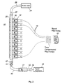
- the present invention provides an electro-optic interconnect or device, generally designated by the numeral 10.
- the electro-optic interconnect 10 comprises a small area high speed photodetector 12 that converts an optical signal into an electrical signal having a magnitude depending upon the amount of light incident on it, and has an intrinsic response time of 5 ps.
- a bias voltage +V is applied across its electrodes 13 and 15 that are separated by a guardrail 17.
- the detector may be a photocathode microchannel, a superconducting detector or any other photoactivated compound device.
- the device 10 includes two optoelectronic detectors 12.
- FIG. 2 shows one of the optoelectronic detectors 12 in detail.
- An optical fiber 14 is attached to the detector and propagates an optical beam or signal 16 onto the detector 12.
- An electro-optic crystal 20 or waveguide extends longitudinally in an orientation orthogonal to the detector 12.
- the crystal 20 is formed from an electro-optic material (for example LiTaO 3 , LiNiO 3 , GaAs, or birefringent polymers), and as will be described with the birefringent axis properly oriented with respect to the electric field and an optical probe beam, shown diagrammatically by the arrow 22.
- a probe laser 24 generates the probe beam, or reading beam, longitudinally through a single mode optical fiber 26 and the crystal 20.
- the probe beam is preferably a continuous wave beam to provide real time signal processing.
- a microwave stripline 30 formed on a nonconducting substrate 32 extends perpendicularly to and supports the crystal 20 and propagates the electrical signal developed by the photodetector 12 to interact with the optical probe beam 22.
- the stripline 30 is terminated in a 50 ohm load 34 to prevent reflections from propagating back down the stripline which would degrade the temporal resolution.
- the substrate 32 is connected to the ground to prevent noise or extraneous signals from interfering with the electric sighal on stripline 30.
- the electrical signal carried by the stripline 30 generates an electric field shown diagrammatically by the curved arrows 38 that penetrates into the underside of the electro-optic crystal 20 inducing a time dependent polarization rotation or phase change on the probe beam 22.
- This change varies with the electric field strength and therefore with the intensity of the light incident on the photodetector.
- the rotation depends on the crystal axis orientation relative to the electric field 38 created by the stripline signal.
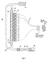
- an array of optoelectronic detectors is shown.
- the optoelectronic detectors in the array are identical to the photodetector shown in FIG. 1.
- the numerals 1-m there are m detectors in the array, each having an end attached to one fiber 14 of the array of optical fibers 52.
- Each fiber 14 propagates an optical beam onto one detector 12.
- Each signal from the two photodetectors 12 contributes to the total polarization rotation of the probe beam 22.
- These additive or subtractive changes are converted to an amplitude modulated signal on the fiber 22 with a ⁇ /2 waveplate 42 and a polarizer 44.
- the ⁇ /2 waveplate 42 can be adjusted to either homodyne or heterodyne the response. In heterodyne operation, the waveplate 42 is adjusted to allow some of the unmodulated probe beam 22 to pass through the waveplate. This sets up a local field that mixes with the signal and is used for linear operation.
- the polarizer 44 converts the polarization rotation induced on the probe beam 22 to a time dependent amplitude modulation. For homodyne operation the waveplate 42 is adjusted and the polarizer 44 is crossed so no light leaks through when there is no voltage developed on a photodetector 12. For both heterodyne and homodyne operation, the polarizer 44 analyzes changes in the phase and polarization of the probe beam 22 produced by the electro-optic effect.
- a probe high speed photodetector 51 converts the amplitude modulated probe beam into a resultant electrical signal on conductor 52 to an output 54 for application to a signal processor 56. This represents the sum of the in-phase optical signals 16 projected through the fibers 14.
- Each of the signal photodetectors 12 contribute to the total polarization rotation of the probe beam 22.
- optical signals on the optical fiber 14 propagate the optical signal to its optoelectronic detector 12.
- the detector 12 converts the optical signal into an electrical signal.
- the electrical signal is propagated down the stripline 30 tc the 50 ohm load 34.
- the propagating electrical signal creates an electric field 38 outside the stripline 30.
- the electric field penetrates into the surface of the electro-optic crystal 20 and induces a time dependent polarization rotation or phase change on the probe beam 22.
- Each detector 12 induces a rotation or phase change corresponding to the received optical signal carried to it by its optical fiber, which are either additive or subtractive.
- the ⁇ /2 waveplate 42 and polarizer 44 are adjusted to convert the total rotation or phase change to a resultant probe beam into a time dependent modulated optical signal.
- the probe high speed detector 50 converts this into an electrical signal representative of the optical signals. This is applied to the signal processor 56 which demodulates and further processes the electrical signal as desired.
- Another technique for selecting whether to configure a photodetector in the summing mode or the subtractive mode is by changing the polarity of the bias voltage on the photodetector.
- a bias voltage +V is applied to the electrodes 13 and 15 of the photodetector.
- a nonconducting guardrail 17 separates the electrodes.
- the two photodetectors are biased identically.
- the polarity of the bias voltage is reversed. This may also require that the photodetector be changed from a pnp type to an npn type device.
- FIG. 3 An alternative embodiment of the electro-optic interconnect is illustrated in FIG. 3. Many of the elements of the interconnect 70 are identical to like parts in the interconnect illustrated in FIG. 2 described above, and accordingly, there have bee applied to each part of the interconnect in FIG. 3 a reference numeral corresponding to the reference numeral that was applied to the like part of the interconnect described above and shown in FIG. 2.
- the fundamental difference between the interconnect shown in FIG. 3 and the interconnect shown in FIG. 2 is that it comprises a Mach-Zehnder interferometer 72 and thus employs phase modulation. Accordingly, it does not incorporate a ⁇ /2 waveplate or polarizer. Each signal photodetector contributes to the total phase change of the probe beam 22.
- the fiber based Mach-Zehnder interferometer 72 comprises a reference leg 74 and an adjustable leg 76 which comprises the path of the probe beam through the electro-optic crystal 20. As was described, passage of the probe beam through the crystal varied depending on the electric signals produced by the optoelectronic detectors and their striplines.
- the system and method of this invention can utilize many other types of optical interferometers.
- the optical interferometer splits light into two separate optical paths and then recombines this light interferometrically to create optical outputs that can present constructive and destructive interference.
- the wavelength of light and the relative optical path lengths of the two legs in the interferometer determine the particular state of interference that takes place when the light is combined. This state of interference determines if the output, or destructive interference, in which case there is an absence of optical intensity output.
- the interferometer 72 serves to translate this phase change into a time dependent amplitude modulation which is detected by the probe high speed photodetector 51.
- the light on the optoelectronic detector 12 propagated by the optical fibers 14 in turn causes a phase delay in the probe beam.
- no phase delay occurs. This consequently unbalances the interferometer 72 and provides a signal to the photodetector 51.
- FIG. 4 An alternative embodiment of the fundamental optoelectronic interconnect 10 is illustrated in FIG. 4 and designated by the numeral 100. This is known as an electro-optic velocity matched configuration. Many of its elements are identical to like parts in the interconnect 10 in FIGs. 1 and 2 described above, and accordingly, there have been applied to each part of the interconnect in FIG. 4 a reference numeral corresponding to the reference numeral that was applied to the like part of the interconnect described above and shown in FIG. 1.
- the electrical signal 102 and the probe beam 22 propagate in the same direction, comprises a velocity matched photodetector 104 that is preferably one that is available from the University of Rochester, and is back illuminated by the optical signal.
- the signal is transmitted through the optical fiber 14 and the substrate 32 to the detector 104. This facilitates connection of the optical fiber to the detector.
- the fiber it is desired to have the fiber as close as possible to the detector. It has been found that for ultraviolet wavelengths of the signal beam, back illumination works best, otherwise front illumination is used.
- the signal beam is transmitted through the optical fiber 14 and the substrate 32 material to the photodetector 104.
- This produces an electrical pulse which propagates down the microwave stripline 30 to the terminator 34.
- the propagating electric field 38 penetrates into the electro-optic crystal 20 inducing a time dependent polarization rotation or phase change on the probe beam.
- the electrical signal 102 and the optical probe beam 22 propagate in the same direction leading to smaller transit time broadening (high frequency response) and/or longer effective crystal lengths (increased modulation depth of the probe beam).
- the time compensated methodology provides a means for correcting optical delays which occur in a serial reading beam geometry due to the time required for the reading optical beam to propagate.
- This propagation time t nd/c, where n is the material index of refraction, d is the distance, and c is the speed of light.
- n the material index of refraction
- d the distance
- c the speed of light.
- n the material index of refraction
- d the distance
- c the speed of light.
- the arrival of the signal beam at the photodetectors is made to be synchronous (either on a row by row as shown in FIG. 5, or element by element basis as shown in FIG. 6) with the arrival of the reading (probe) beam so that propagation delays do not accumulate. This avoids degrading the bandwidth. This is accomplished by inserting equivalent (compensating) optical delays in a prescribed manner into the signal beams.
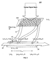
- FIG. 5 shows a one dimensional time compensation system for a serial optoelectronic reading device, generally illustrated by the numeral 200.
- the optical signal arrives at a time compensation element (TCE) 202.
- TCE time compensation element
- the TCE 202 comprises an optical wedge of the kind that is commercially available from several optical device manufacturers.
- the optical wedge is configured as an m x i matrix. As the TCE 202 lies in front of the optical fiber array 52.
- t cm is the time delay in row m of the TCE 202
- n f is the index of refraction of the optical fiber 14
- d fmi is the length of the optical fiber in row m and column i
- c is the speed of light.
- the probe beam 22 and the signal beam 16 accumulate a temporal error equal to n 1 d 11mi /c which degrades the array's temporal resolution.
- each row is compensated. More particularly, the center element in each row is synchronized with the probe beam 22. Note the other elements in each row are not synchronized. Thus, this technique has some temporal resolution error associated with it, which would be analogous to time jitter.
- the one dimensional time compensation scheme allows the number of fibers to be squared (i.e., 10 fibers becomes 100 fibers) with the same temporal resolution (frequency bandwidth).
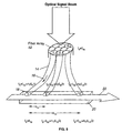
- FIG. 6 shows an element by element time compensation architecture.
- the probe beam 22 and signal beam 16 accumulate a temporal error equal to n 1 d 1m /c which degrades the array's temporal resolution.
- this embodiment does not degrade the optical reading of the probe beam.
- an optoelectronic interconnect 300 is illustrated. As shown, there are separate optoelectronic arrays, one for addition 302 and one for subtraction 304.
- a modulator 18 is included in one arm and provides phase or polarization to the optical signal. Accordingly, the modulation can be adjusted to make the signals in-phase or out-of-phase by 180°. In-phase signals are additive and out-of-phase signals are subtractive.
- the difference in the function of the arrays 302 and 304 results either from a change in the electro-optic orientation of the crystal 20 relative to the photodetector propagating electric field 38, a change in the semiconductor structure of the photodetector 12 to allow for an inversion of the bias voltage (from positive voltage to negative voltage), or the insertion of an electro-optic modulator 18 (phase or polarization) before and/or after one of the photodetector arrays 302.
- the signal on each individual fiber 14 in the array 52 is either routed to the positive or negative photodetector array with an electro-optic modulator 306 and polarizer 308.
- Passive time compensation architectures need to be incorporated into the signal fiber array in order to synchronize the probe 22 and photodetector electric field 38 at each point in the interconnect 300.
- Active time or nonsynchronous passive compensation architectures can be implemented to provide additional functional capability (for example, dynamically controlled probe sequences) or environmental corrections.
- the interconnect may be operable with amplitude or phase/polarization rotation embodiments.
- FIG. 8 shows an electro-optic arithmetic interconnect 350.
- an electro-optic modulator 18 phase or polarization
- These additional modulators can electrodes 352 and 354 along the appropriate crystal axis and applying a voltage across the crystal 20.
- These additional modulators 18 can either be resonant or traveling wave devices. The application of voltage across these electrodes 352 and 354 will in effect alter the polarization (phase) of the probe beam 22 so that addition or subtraction can occur at each separate photodetector 12.
- Passive time compensation architectures as shown in FIGs. 5 and 6 need to be incorporated into the signal fiber array in order to synchronize the probe and photodetector electric field at each point in the interconnect. Active or nonsynchronous passive time compensation architectures can be implemented to provide additional functional capability (for example, dynamically controlled probe sequences) or environmental corrections.
- the interconnect may be operable amplitude or phase/polarization rotation embodiments.
- an electro-optic interconnect that can be configured for adding and subtracting optical signals is provided.
Landscapes
- Physics & Mathematics (AREA)
- Nonlinear Science (AREA)
- General Physics & Mathematics (AREA)
- Optics & Photonics (AREA)
- Chemical & Material Sciences (AREA)
- Engineering & Computer Science (AREA)
- Ceramic Engineering (AREA)
- Crystallography & Structural Chemistry (AREA)
- Measuring Instrument Details And Bridges, And Automatic Balancing Devices (AREA)
- Optical Communication System (AREA)
- Optical Modulation, Optical Deflection, Nonlinear Optics, Optical Demodulation, Optical Logic Elements (AREA)
- Measurement Of Current Or Voltage (AREA)
Abstract
Description
Claims (7)
- An electro-optic interconnect for use with a probe beam and optical signals comprising:a plurality of first optoelectronic detectors, each being responsive to an optical signal and operative to develop a first electrical signal; andan electro-optic device for propagating a probe beam and having a propagation characteristic that changes in response to an electrical signal, and being responsive to said plurality of first electrical signals which serve to change the propagation characteristic and being operative to develop a second signal corresponding to the information contained in the received optical signal.
- An electro-optic interconnect for receiving optical signals containing information and a probe beam comprising:a plurality of first optoelectronic detector means, each being responsive to an optical signal and operative to develop a plurality of electrical signals, each representing a portion of the information;means for generating an optical probe beam;means responsive to said plurality of electrical signals and operative to change a characteristic of said optical probe beam corresponding to the information; anda second optoelectronic detector responsive to the changed characteristic and operative to develop an output electrical signal representative of the information contained in said optical signals.
- The electro-optic interconnect as recited in claim 2 wherein said means responsive to said plurality of electrical signals comprises means for propagating said optical probe beam.
- The electro-optic interconnect as recited in claim 3 wherein said means for propagating comprises an electro-optic crystal.
- The electro-optic interconnect receiver as recited in claim 2 wherein said each of said plurality of first optoelectronic detector means comprises an optoelectronic detector and a stripline.
- The electro-optic interconnect as recited in claim 2 and further comprising an interferometer having an adjustable leg and a reference leg, each receiving said optical probe beam, and wherein said adjustable leg responds to said plurality of electrical signals to change the phase of said optical probe beam relative to the phase of said optical probe beam propagating through said reference leg.
- The electro-optic interconnect as recited in claim 2 wherein said plurality of first optoelectronic detector means serves to add the optical signals, and further comprising a plurality of third optoelectronic detector means configured to subtract the optical signals propagated thereto.
Applications Claiming Priority (2)
| Application Number | Priority Date | Filing Date | Title |
|---|---|---|---|
| US586014 | 1984-03-05 | ||
| US09/586,014 US6624922B1 (en) | 2000-06-02 | 2000-06-02 | Electro-optic device for adding/subtracting optical signals |
Publications (2)
| Publication Number | Publication Date |
|---|---|
| EP1160615A2 true EP1160615A2 (en) | 2001-12-05 |
| EP1160615A3 EP1160615A3 (en) | 2003-11-19 |
Family
ID=24343939
Family Applications (1)
| Application Number | Title | Priority Date | Filing Date |
|---|---|---|---|
| EP01111970A Withdrawn EP1160615A3 (en) | 2000-06-02 | 2001-05-21 | Electro-optic device for adding/subtracting optical signals |
Country Status (3)
| Country | Link |
|---|---|
| US (1) | US6624922B1 (en) |
| EP (1) | EP1160615A3 (en) |
| JP (1) | JP2002006357A (en) |
Cited By (1)
| Publication number | Priority date | Publication date | Assignee | Title |
|---|---|---|---|---|
| CN117263806A (en) * | 2023-08-15 | 2023-12-22 | 福泉环保城发展有限公司 | A kind of synthesis method of tetraethylammonium bromide |
Families Citing this family (4)
| Publication number | Priority date | Publication date | Assignee | Title |
|---|---|---|---|---|
| US7224981B2 (en) * | 2002-06-20 | 2007-05-29 | Intel Corporation | Speech recognition of mobile devices |
| US7525723B2 (en) * | 2006-06-30 | 2009-04-28 | Intel Corporation | Circuit board-to-circuit board connectors having electro-optic modulators |
| US20080122463A1 (en) * | 2006-06-30 | 2008-05-29 | Sanjay Dabral | Testing microelectronic devices using electro-optic modulator probes |
| JP7097548B2 (en) * | 2018-03-02 | 2022-07-08 | 日本電信電話株式会社 | Optical digital-to-analog converter |
Family Cites Families (10)
| Publication number | Priority date | Publication date | Assignee | Title |
|---|---|---|---|---|
| US4236243A (en) * | 1978-04-20 | 1980-11-25 | National Research Development Corporation | Telecommunication systems |
| JPS6134526A (en) * | 1984-07-26 | 1986-02-18 | Omron Tateisi Electronics Co | Optical comparator |
| US4773739A (en) * | 1986-03-05 | 1988-09-27 | Hughes Aircraft Company | Self-pumped phase conjugate mirror and method using AC-field enhanced photorefractive effect |
| US5229878A (en) * | 1990-07-02 | 1993-07-20 | Canon Kabushiki Kaisha | Method and apparatus for modulating light using semiconductor element having quantum well structure |
| JP2935478B2 (en) * | 1991-02-28 | 1999-08-16 | キヤノン株式会社 | Pure optical light modulator |
| JPH05241220A (en) * | 1992-02-28 | 1993-09-21 | Kokusai Denshin Denwa Co Ltd <Kdd> | Optical logic element |
| EP0606170A3 (en) * | 1993-01-07 | 1996-11-20 | Nec Corp | Optical transmission system and optical network terminals used therein. |
| US5832148A (en) * | 1995-12-20 | 1998-11-03 | California Institute Of Technology | Electrically controlled wavelength multiplexing waveguide filter |
| US5909303A (en) * | 1996-01-04 | 1999-06-01 | The Board Of Trustees Of The Leland Stanford Junior University | Optical modulator and optical modulator array |
| JP3458613B2 (en) * | 1996-09-04 | 2003-10-20 | Kddi株式会社 | Wavelength conversion device and optical operation device |
-
2000
- 2000-06-02 US US09/586,014 patent/US6624922B1/en not_active Expired - Fee Related
-
2001
- 2001-05-21 EP EP01111970A patent/EP1160615A3/en not_active Withdrawn
- 2001-05-25 JP JP2001156276A patent/JP2002006357A/en active Pending
Cited By (1)
| Publication number | Priority date | Publication date | Assignee | Title |
|---|---|---|---|---|
| CN117263806A (en) * | 2023-08-15 | 2023-12-22 | 福泉环保城发展有限公司 | A kind of synthesis method of tetraethylammonium bromide |
Also Published As
| Publication number | Publication date |
|---|---|
| US6624922B1 (en) | 2003-09-23 |
| EP1160615A3 (en) | 2003-11-19 |
| JP2002006357A (en) | 2002-01-09 |
Similar Documents
| Publication | Publication Date | Title |
|---|---|---|
| EP0977022B1 (en) | Optical waveguide vibration sensor system for remote detection | |
| US20200174188A1 (en) | Polarization Independent Processing in Integrated Photonics | |
| US4644145A (en) | Optical receiver with electrically variable attenuator | |
| US12111396B2 (en) | Device and method for scanning frequency-modulated continuous wave (FMCW) LiDAR range measurement | |
| JP3886147B2 (en) | Dispersion compensation | |
| CA1280170C (en) | Homodyne interconnections of integrated circuits | |
| US4815853A (en) | Three-axis fiber-optic ring interferometer | |
| US5721637A (en) | Wavelength converter apparatus | |
| US7274437B2 (en) | Laser detection and ranging apparatus | |
| EP1161006B1 (en) | Optoelectronic communication system in turbulent medium having array of photodetectors and time compensation | |
| US6624922B1 (en) | Electro-optic device for adding/subtracting optical signals | |
| US6580540B1 (en) | Time compensation architectures for controlling timing of optical signals | |
| US11327226B2 (en) | Integrated photonics long-distance sensing system | |
| US6516103B1 (en) | Optical interconnect capable of performing addition/subtraction | |
| US20260063469A1 (en) | Photonic integrated circuit chip for distributed acoustic sensing | |
| JP3632714B2 (en) | Electromagnetic wave receiving system | |
| US11838059B2 (en) | Optical assembly and method for optical signal processing | |
| JP3318706B2 (en) | Sensing device | |
| JPH0643411A (en) | Method and apparatus for controlling operating point of optical modulator | |
| JP3505669B2 (en) | Electric field sensor | |
| Shah | Phase stabilization of microwave reference signals in analog fiber-optic links | |
| Hunsperger | Applications of Integrated Optics and Current Trends | |
| Al-Raweshidy et al. | Predetection correlation in a spread-spectrum multiplexing system for fiber optic interferometers | |
| JP2000249734A (en) | Sensing device | |
| Hunsperger | Applications of Integrated Optics and Current Trends |
Legal Events
| Date | Code | Title | Description |
|---|---|---|---|
| PUAI | Public reference made under article 153(3) epc to a published international application that has entered the european phase |
Free format text: ORIGINAL CODE: 0009012 |
|
| AK | Designated contracting states |
Kind code of ref document: A2 Designated state(s): AT BE CH CY DE DK ES FI FR GB GR IE IT LI LU MC NL PT SE TR |
|
| AX | Request for extension of the european patent |
Free format text: AL;LT;LV;MK;RO;SI |
|
| PUAL | Search report despatched |
Free format text: ORIGINAL CODE: 0009013 |
|
| AK | Designated contracting states |
Kind code of ref document: A3 Designated state(s): AT BE CH CY DE DK ES FI FR GB GR IE IT LI LU MC NL PT SE TR |
|
| AX | Request for extension of the european patent |
Extension state: AL LT LV MK RO SI |
|
| RAP1 | Party data changed (applicant data changed or rights of an application transferred) |
Owner name: NORTHROP GRUMMAN CORPORATION |
|
| RIC1 | Information provided on ipc code assigned before grant |
Ipc: 7H 04J 14/08 B Ipc: 7G 02F 3/00 B Ipc: 7G 02F 1/225 B Ipc: 7G 02F 1/035 A |
|
| RAP1 | Party data changed (applicant data changed or rights of an application transferred) |
Owner name: NORTHROP GRUMMAN CORPORATION |
|
| 17P | Request for examination filed |
Effective date: 20040514 |
|
| AKX | Designation fees paid |
Designated state(s): DE FR GB IT |
|
| STAA | Information on the status of an ep patent application or granted ep patent |
Free format text: STATUS: THE APPLICATION IS DEEMED TO BE WITHDRAWN |
|
| 18D | Application deemed to be withdrawn |
Effective date: 20071201 |