EP1158671A2 - Acoustic mirror materials for acoustic devices - Google Patents
Acoustic mirror materials for acoustic devices Download PDFInfo
- Publication number
- EP1158671A2 EP1158671A2 EP01610050A EP01610050A EP1158671A2 EP 1158671 A2 EP1158671 A2 EP 1158671A2 EP 01610050 A EP01610050 A EP 01610050A EP 01610050 A EP01610050 A EP 01610050A EP 1158671 A2 EP1158671 A2 EP 1158671A2
- Authority
- EP
- European Patent Office
- Prior art keywords
- acoustic
- impedance
- reflector stack
- layer
- stack
- Prior art date
- Legal status (The legal status is an assumption and is not a legal conclusion. Google has not performed a legal analysis and makes no representation as to the accuracy of the status listed.)
- Granted
Links
- 239000000463 material Substances 0.000 title claims abstract description 109
- VYPSYNLAJGMNEJ-UHFFFAOYSA-N Silicium dioxide Chemical compound O=[Si]=O VYPSYNLAJGMNEJ-UHFFFAOYSA-N 0.000 claims abstract description 92
- 229910052681 coesite Inorganic materials 0.000 claims abstract description 45
- 229910052906 cristobalite Inorganic materials 0.000 claims abstract description 45
- 239000000377 silicon dioxide Substances 0.000 claims abstract description 45
- 229910052682 stishovite Inorganic materials 0.000 claims abstract description 45
- 229910052905 tridymite Inorganic materials 0.000 claims abstract description 45
- 239000004964 aerogel Substances 0.000 claims abstract description 17
- 238000004519 manufacturing process Methods 0.000 claims abstract description 11
- 239000000758 substrate Substances 0.000 claims description 19
- 238000005229 chemical vapour deposition Methods 0.000 claims description 15
- 238000000034 method Methods 0.000 claims description 8
- 238000004544 sputter deposition Methods 0.000 claims description 7
- GWEVSGVZZGPLCZ-UHFFFAOYSA-N Titan oxide Chemical compound O=[Ti]=O GWEVSGVZZGPLCZ-UHFFFAOYSA-N 0.000 claims description 6
- PNEYBMLMFCGWSK-UHFFFAOYSA-N aluminium oxide Inorganic materials [O-2].[O-2].[O-2].[Al+3].[Al+3] PNEYBMLMFCGWSK-UHFFFAOYSA-N 0.000 claims description 6
- 229910052593 corundum Inorganic materials 0.000 claims description 6
- 239000010409 thin film Substances 0.000 claims description 6
- 229910001845 yogo sapphire Inorganic materials 0.000 claims description 6
- 229910019878 Cr3Si Inorganic materials 0.000 claims description 4
- 229910002785 ReO3 Inorganic materials 0.000 claims description 4
- 238000000151 deposition Methods 0.000 claims description 4
- YSZJKUDBYALHQE-UHFFFAOYSA-N rhenium trioxide Chemical compound O=[Re](=O)=O YSZJKUDBYALHQE-UHFFFAOYSA-N 0.000 claims description 4
- 229910019802 NbC Inorganic materials 0.000 claims description 3
- 229910004166 TaN Inorganic materials 0.000 claims description 3
- 229910034327 TiC Inorganic materials 0.000 claims description 3
- 229910052594 sapphire Inorganic materials 0.000 claims description 3
- 239000010980 sapphire Substances 0.000 claims description 3
- 229910052710 silicon Inorganic materials 0.000 claims description 3
- 239000010703 silicon Substances 0.000 claims description 3
- 229910003468 tantalcarbide Inorganic materials 0.000 claims description 3
- 239000011521 glass Substances 0.000 claims description 2
- 239000010453 quartz Substances 0.000 claims description 2
- 239000000126 substance Substances 0.000 claims description 2
- 239000010408 film Substances 0.000 description 13
- 238000005240 physical vapour deposition Methods 0.000 description 11
- 238000000926 separation method Methods 0.000 description 10
- 229910052581 Si3N4 Inorganic materials 0.000 description 8
- 239000004020 conductor Substances 0.000 description 5
- 239000012528 membrane Substances 0.000 description 5
- 230000004044 response Effects 0.000 description 5
- 239000012212 insulator Substances 0.000 description 4
- 230000010287 polarization Effects 0.000 description 4
- 238000004891 communication Methods 0.000 description 3
- 230000008878 coupling Effects 0.000 description 3
- 238000010168 coupling process Methods 0.000 description 3
- 238000005859 coupling reaction Methods 0.000 description 3
- 238000013461 design Methods 0.000 description 3
- 239000000499 gel Substances 0.000 description 3
- 239000002002 slurry Substances 0.000 description 3
- BOTDANWDWHJENH-UHFFFAOYSA-N Tetraethyl orthosilicate Chemical compound CCO[Si](OCC)(OCC)OCC BOTDANWDWHJENH-UHFFFAOYSA-N 0.000 description 2
- 238000013459 approach Methods 0.000 description 2
- 230000001413 cellular effect Effects 0.000 description 2
- 239000000615 nonconductor Substances 0.000 description 2
- 230000003071 parasitic effect Effects 0.000 description 2
- 239000011343 solid material Substances 0.000 description 2
- 230000026683 transduction Effects 0.000 description 2
- 238000010361 transduction Methods 0.000 description 2
- LFQSCWFLJHTTHZ-UHFFFAOYSA-N Ethanol Chemical compound CCO LFQSCWFLJHTTHZ-UHFFFAOYSA-N 0.000 description 1
- 229910025794 LaB6 Inorganic materials 0.000 description 1
- 239000004965 Silica aerogel Substances 0.000 description 1
- 239000003377 acid catalyst Substances 0.000 description 1
- 229910001632 barium fluoride Inorganic materials 0.000 description 1
- 230000009286 beneficial effect Effects 0.000 description 1
- 239000013590 bulk material Substances 0.000 description 1
- 239000003990 capacitor Substances 0.000 description 1
- 230000008859 change Effects 0.000 description 1
- 239000013078 crystal Substances 0.000 description 1
- 230000001419 dependent effect Effects 0.000 description 1
- 230000008021 deposition Effects 0.000 description 1
- 238000011161 development Methods 0.000 description 1
- 238000001035 drying Methods 0.000 description 1
- 230000000694 effects Effects 0.000 description 1
- 238000005516 engineering process Methods 0.000 description 1
- 230000005284 excitation Effects 0.000 description 1
- 238000001914 filtration Methods 0.000 description 1
- 239000006260 foam Substances 0.000 description 1
- 229910052809 inorganic oxide Inorganic materials 0.000 description 1
- 230000003993 interaction Effects 0.000 description 1
- 238000010295 mobile communication Methods 0.000 description 1
- 238000012986 modification Methods 0.000 description 1
- 230000004048 modification Effects 0.000 description 1
- 239000011368 organic material Substances 0.000 description 1
- 239000002243 precursor Substances 0.000 description 1
- 230000008569 process Effects 0.000 description 1
- 230000009467 reduction Effects 0.000 description 1
- 238000011160 research Methods 0.000 description 1
- 239000004065 semiconductor Substances 0.000 description 1
- 239000008257 shaving cream Substances 0.000 description 1
- 238000005549 size reduction Methods 0.000 description 1
- 239000007787 solid Substances 0.000 description 1
- 239000002904 solvent Substances 0.000 description 1
- 238000001228 spectrum Methods 0.000 description 1
- 229910001637 strontium fluoride Inorganic materials 0.000 description 1
- FVRNDBHWWSPNOM-UHFFFAOYSA-L strontium fluoride Chemical compound [F-].[F-].[Sr+2] FVRNDBHWWSPNOM-UHFFFAOYSA-L 0.000 description 1
- 230000002889 sympathetic effect Effects 0.000 description 1
- 230000002277 temperature effect Effects 0.000 description 1
- UONOETXJSWQNOL-UHFFFAOYSA-N tungsten carbide Chemical compound [W+]#[C-] UONOETXJSWQNOL-UHFFFAOYSA-N 0.000 description 1
- XLYOFNOQVPJJNP-UHFFFAOYSA-N water Substances O XLYOFNOQVPJJNP-UHFFFAOYSA-N 0.000 description 1
Images


Classifications
-
- H—ELECTRICITY
- H03—ELECTRONIC CIRCUITRY
- H03H—IMPEDANCE NETWORKS, e.g. RESONANT CIRCUITS; RESONATORS
- H03H9/00—Networks comprising electromechanical or electro-acoustic elements; Electromechanical resonators
- H03H9/15—Constructional features of resonators consisting of piezoelectric or electrostrictive material
- H03H9/17—Constructional features of resonators consisting of piezoelectric or electrostrictive material having a single resonator
- H03H9/171—Constructional features of resonators consisting of piezoelectric or electrostrictive material having a single resonator implemented with thin-film techniques, i.e. of the film bulk acoustic resonator [FBAR] type
- H03H9/172—Means for mounting on a substrate, i.e. means constituting the material interface confining the waves to a volume
- H03H9/175—Acoustic mirrors
Definitions
- the present invention relates to bulk acoustic wave devices such as acoustic resonators, and more particularly to acoustic mirror materials used in these devices.
- Piezoelectric crystals have provided the basis for bulk acoustic wave devices for filtering or frequency control such as oscillators, acoustic resonators and filters, operating at very high radio frequencies (on the order of several gigahertz).
- filters such as band pass and/or band stop filters are based on dielectric-filled electromagnetic cavity resonators with physical dimensions that are large, since they are dictated by the wavelength of the resonating electromagnetic wave. Due to the interaction between electrical charge, stress, and strain in a piezoelectric material, such material acts as a transducer, which converts energy back and forth between electromagnetic and acoustic (i.e., mechanical) energy. Thus, a piezoelectric material incorporated in a structure designed to have a strong mechanical resonance provides an electrically resonant device.
- the velocity of an acoustic wave is approximately 1/10000 that of the velocity of an electromagnetic wave. This relationship between the wave's velocity and device dimensions thus allows a reduction of roughly this factor in the size of certain devices, including acoustic resonators, employing this material.
- an electrical filter based on acoustic waves may be much smaller than one based on electromagnetic waves.
- a mechanical material that transduces between electromagnetic and mechanical energies For example, such may be a piezoelectric, magnetostrictive or electrostrictive material.
- TFR component 100 includes a piezoelectric material 110 interposed between two conductive electrode layers 105 and 115, with electrode layer 115 formed on a support structure 120.
- the support structure 120 can be a plurality of alternating reflecting layers (acoustic mirrors) provided on a solid semiconductor substrate which may be made of silicon, sapphire, glass or quartz, for example.
- the support structure 120 can alternatively be removed after device fabrication leaving a free standing membrane type device.
- the piezoelectric material is commonly selected from the group comprising at least ZnO, CdS and AlN.
- Electrode layers 105 and 115 are generally formed from a conductive material, such of Al, but may be formed from other conductors as well.
- TFR filter circuits may be employed in cellular, wireless and fiber-optic communications, as well as in computer or computer-related information-exchange or information-sharing systems.
- any sympathetic vibration or mode has a response curve showing how at a certain frequency the amplitude of mechanical response goes through a peaked maximum for fixed excitation strength.
- an electrical current response peak where the film produces a maximum current for a fixed voltage since the mechanical motion produces charge at the surface of the piezo. This peak defines the "zero" resonant frequency of a acoustic resonator (i.e., the term refers to the zero or low impedance to the flow of current.)
- the piezoelectric film also produces a polarization current like a capacitor, since it is a dielectric. This current increases linearly with frequency for a fixed voltage, and since the mechanical resonance is narrow (about 1 part in 100 changes in frequency) the polarization current can be essentially thought of as constant while the piezoelectric current goes through its peak.
- the pole frequency is the frequency at which the piezoelectric and polarization currents most nearly or substantially cancel each other out. Since the piezoelectric current has a peak and reverses its polarity through resonance, its value essentially cancels that of the nearly constant polarization current at one frequency--the pole frequency. Therefore, the separation between pole and zero resonant frequencies is dependent in one respect on the properties of the piezoelectric material, and the mechanical resonance that is explained in more detail below.
- the separation in frequency between pole and zero resonant frequencies in an acoustic device such as a TFR is determined by properties of the piezoelectric film, and more particularly by the mechanical and electrical properties and/or characteristics of the piezoelectric.
- the fractional separation is about 3% of the resonance frequency for a plate geometry suspended in air, such as in a membrane type TFR (e.g. the lateral dimension is large as compared to the film's thickness).
- Fig. 2 illustrates a conventional Bragg reflector stack constituting acoustic mirror layers of an acoustic device such as a TFR.
- the reflecting stack 125 of Fig. 2 corresponds somewhat to substrate 120 of Fig. 1, and illustrates the make up of the acoustic mirrors in more detail.
- the conventional acoustic mirror arrangement or Bragg reflecting stack 125 comprises a plurality of alternating mirror layers of a high acoustic impedance material, such as AlN layers 130a-d, and a low acoustic impedance material such as SiO 2 layers 135a-d, that are provided on a substrate 140 such as silicon, for example.
- Other conventional reflecting stacks used in acoustic devices such as TFRs typically include acoustic mirror layer combinations of Si 3 N 4 ⁇ x /SiO 2 as well.
- Acoustic impedance is the product of a material's density and speed. This relation is important because, as a sound wave passes between two unlike materials, the portion of the wave reflected by the interface therebetween is larger for a greater difference in impedance between the differing materials. Accordingly, a common theme of the inventors is that, in order to fabricate a good acoustic mirror, and hence acoustic resonant device, it is desirable to place materials having as dissimilar impedance as possible against each other for maximal reflections.
- acoustic resonator devices such as TFRs with the reflecting stack 125 illustrated in Fig. 2.
- the mechanical resonance, and hence the piezoelectric current response peak of the resonator is altered when a device is fabricated on an acoustic mirror, as compared to the case where the device is fabricated as a membrane.
- the pole frequency is reduced to a value closer to the zero frequency of the resonator.
- the current acoustic mirror arrangement requires a substantial number of alternating reflective layers, providing for a bulkier resonator device that requires longer manufacturing process time and cost. This is because the number of layers required depends on the degree of acoustic mismatch between them, and the AlN/SiO 2 and Si 3 N 4 ⁇ x /SiO 2 layer combinations currently used do not represent the highest possible impedance mismatch. To restate, at each interface there is a reflection of energy; and if each reflection is weak because of poor impedance mismatch, more layers are therefore required to achieve the total desired reflection.
- Air presents an enormous impedance mismatch with any solid material, simply because its density is typically a factor of at least 1000 lower than the density of the adjacent solid material.
- Maximal impedance mismatch is also important, albeit to a lesser extent, for the interfaces between each pair of subsequent mirror layers, since it is always beneficial to have a large acoustic impedance mismatch, when maximum bandwidth and fewer required layers are desired.
- a reflecting stack for an acoustic device which can attain the highest possible impedance mismatch between the reflecting layers of the stack so as to maximize bandwidth, and which reduces manufacturing costs by requiring fewer layers for the device, as compared to conventional acoustic mirrors.
- the present invention provides a reflector stack for an acoustic device which comprises alternating layers of materials having a substantial acoustic impedance mismatch therebetween.
- the reflecting stack incorporates higher impedance layers of material that are determined based on the elastic constants and density of the materials, with known low impedance material layers to achieve a desired large mismatch.
- the reflecting stack is formed from a low density material that is deposited by chemical vapor deposition (CVD) and/or sputtering on a substrate.
- CVD chemical vapor deposition
- the aforementioned higher impedance materials calculated as a function of their elastic constants may be combined with the low density material formed by CVD and/or sputtering to further increase the acoustic impedance mismatch, as well as to reduce the number of mirror layers required in the reflecting stack of the acoustic device.
- the present invention provides a reflecting stack or acoustic mirror arrangement for an acoustic device, which may attain the highest possible impedance mismatch between the reflecting layers of the stack so as to maximize bandwidth, and which may reduce manufacturing costs by requiring fewer layers for the device. as compared to conventional acoustic mirrors.
- the reflecting stack is fabricated in a reduced time to lower cost by incorporating materials providing a larger acoustic impedance mismatch than those currently attainable.
- the bandwidth of the resulting resonator device may be widened, particularly when the sputter-deposited and/or CVD low density material is the topmost layer as deposited in the acoustic mirror of the device.
- a low density (at least about 1.0 g/cm 3 or lower) material was determined from applications which utilize a low density dielectric constant material.
- these materials have low dielectric constants is superfluous, it is the low density characteristics of these materials that is desirable to applications in the aforementioned acoustic devices.
- the same process used to lower the dielectric constant of the low density material may also be used to lower its density, and therefore its impedance. This in turn enables a higher impedance mismatch between layers of the stack to be achieved, of which is particularly crucial between the topmost, or first low density material layer in the mirror arrangement, and the piezoelectric material layer.
- the separation in frequency between pole and zero resonant frequencies in an acoustic device such as a TFR is determined by the mechanical and electrical properties and/or characteristics of the piezoelectric.
- the fractional separation is about 3% of the resonance frequency for a plate geometry suspended in air.
- Alternating low and high acoustic impedance materials of quarter wave thickness transform the impedance of the substrate to a greatly reduced value due to the constructive interference of reflections from boundaries between the many layers. This keeps the acoustic energy favorably trapped and resonant near the piezoelectric layer.
- bigger mismatch between piezo and mirror and/or between mirror complimentary materials results in a widening of the range of frequencies of this effectively lowered acoustic impedance; i.e., it keeps the energy trapped even more favorably in the immediate topmost layers.
- the limit to this desired broad range of low impedance is when air, with its very low impedance, is used instead of a low impedance material as the first layer in the mirror.
- the device loses the advantages of an acoustic device fabricated with an air interface. Since the most important acoustic impedance mismatch is of course the first one, that is, between the piezo film and the first or topmost mirror layer it is desirable to use a low density SiO 2 for the first mirror layer, mounted on a substrate of the acoustic device.
- the reflecting stack incorporates higher impedance layers of piezoelectric material that are determined based on the elastic constants of the materials.
- Table I depicts the results of these calculations, listing the materials selected with their calculated Z.
- Table 1 are listed the specific material, density, elastic constant C 11 , velocity of sound or speed and acoustic impedance Z.
- AlN and Si 3 N 4 ⁇ x have acoustic impedance Z equal to 387 and 284 kg/m 2 s respectively. These materials do not provide the kind of impedance mismatch desired in acoustic devices.
- Such materials include, but are not limited to: Al 2 O 3 , Cr 3 Si, NbC, ReO 3 , TaC, TaN, TiC, TiO 2 , VC, WN, WO 2 and ZrC. Accordingly, these higher Z layers increase the impedance mismatch of the stack, thereby proving a wider attainable bandwidth for the acoustic device.
- WC tungsten carbide
- TFR band pass or band stop filters tungsten carbide
- resonator-based frequency control circuits for example.
- a lower impedance SiO 2 material than that attained by convention physical vapor deposition (PVD) of SiO 2 in the acoustic mirror is provided by depositing the SiO 2 via chemical vapor deposition (CVD) or sputter deposition.
- CVD chemical vapor deposition
- sputter deposition Use of CVD and/or sputtering provides a SiO 2 layer having a lower density (about 1.0 g/cm 3 as compared to about 2.3 g/cm 3 for PVD SiO 2 ).
- the lower density of the CVD/sputtered SiO 2 layer means a lower Z (low impedance) material, which in turn provides a higher acoustic impedance mismatch between the piezo film and bottom layer, as well as between each pair of low impedance SiO 2 layer and adjacent mirror layer of conventional high impedance material.
- the result is a thinner acoustic device requiring fewer mirror layers, which may reduce manufacturing time and production costs.
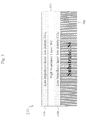
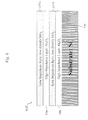
- Figs. 3 and 4 illustrates an acoustic mirror arrangement where the reflector stack is configured as a conductor and insulator respectively, and combine the advantages obtained by the higher impedance layers and low density material layers in accordance with the present invention.
- the acoustic mirror arrangement 225 includes a high Z WC layer 230 (WC is known as a poor electrical insulator) sandwiched between two low density/low Z SiO 2 layers 235a and 235b formed by CVD/Sputtering on a Si substrate 240.
- WC is known as a poor electrical insulator
- unwanted electrical coupling may result from using a conducting stack, but in simpler structures a conducting stack may be acceptable. If such electrical coupling is to be prevented, however, electrically conducting acoustic mirror layers such as the above-noted WC layer 135 should not be used.
- alternating layers of high Z Al 2 O 3 layers 330a and 330b and low density/low Z SiO 2 layers 335a and 335b are formed on Si substrate 340. Both of these materials are known as good electrical insulators.
- the desirable or exemplary non-insulating stack (WC and low density SiO 2 ) of Fig. 3 requires only 11 ⁇ 2 pairs of mirror layers, and the desirable or exemplary insulating stack of Fig. 4 (Al 2 O 3 /poly-crystalline sapphire and low density SiO 2 ) requires only 2 pair of mirror layers.
- the inventors have determined impedance ratios and the required layer pairs needed to satisfy the ratio for several reflector stacks. Evaluated and compared were one stack comprising the conventional AlN/PVD SiO 2 layer configuration (typically used since the ability exists to deposit AlN as the piezo layer and standard SiO 2 is ubiquitous); a second manufactured of a Si 3 N 4 ⁇ x /PVD SiO 2 layer configuration (a poor combination but fabricated from readily available materials); and an AlN/CVD SiO 2 (low density SiO 2 ) layer configuration (conventionally used materials but employing the low density SiO 2 of the present invention, which is not currently used for making TFR devices).
- the conventional AlN/PVD SiO 2 layer configuration typically used since the ability exists to deposit AlN as the piezo layer and standard SiO 2 is ubiquitous
- a second manufactured of a Si 3 N 4 ⁇ x /PVD SiO 2 layer configuration a poor combination but fabricated from readily available materials
- the mirror arrangement has an impedance ratio of about 3:1, which requires 3-4 layer pairs.
- the Si 3 N 4 ⁇ x /PVD SiO 2 layer configuration requires 4-5 layer pairs, since it has only about a 1.5:1 impedance ratio.
- the AlN/CVD SiO 2 (low density SiO 2 ) layer configuration needs only 2-3 layer pairs, due to its advantageous 6:1 impedance ratio. It can be concluded that the inclusion of the CVD/sputter deposited low density SiO 2 in the reflector stack/mirror arrangement provides for a higher impedance mismatch ratio, while requiring fewer layers than a reflector stack containing PVD SiO 2 .
- aerogel or xerogels of SiO 2 provide an even lower impedance material to use in the reflector stack.
- These materials are essentially foams created by the drying of gels in air (xero) or by supercritical solvent removal (aero).
- Aerogel is a light, fog-like substance which generally has the consistency of dried shaving cream, for example.
- the densities of xerogels are typically half those of the corresponding bulk material and those of aerogels can approach that of air itself.
- the terms are often used loosely, with aerogel meaning any very lower density dried gel.
- this discussion addresses silica aerogels, the material may be modified for lower density when air dried, may be based on Al 2 O 3 or other inorganic oxides, or even may be based on organic materials.
- a pre-cursor such as TEOS (tetraethylorthosilicate) is mixed with an acid catalyst such as alcohol and water to form a slurry film.
- the slurry film is then "spun" on the substrate by a well-known lithographic technique similar to that used for applying photo-resist. Once the slurry film has been applied, it is heated to preliminarily congeal it into a jello-like consistency.
- the gel may be dried in air or by a supercritical CO 2 treatment, depending on the desired density (i.e., there is a range of available densities depending on the desired application; thus the aerogel/xerogel layer could have a density of at least 0.3 g/cm 3 , at least 0.5 g/cm 3 , etc.).
- the resultant aerogel film has an extremely low density (as low as 0.1 g/cm 3 ), and is an excellent attenuator of acoustic sound waves.
- the sound velocity is directly proportional to the density.
- sound travels through an aerogel layer of density 0.1 g/cm 3 at a rate of about 170 A/ps, or about 6,000 times slower than sound velocity through a conventional PVD SiO 2 layer.
- the elastic constant C 11 for the aerogel is about 2.7 x 10 6 N/m 2 , whereas for conventional PVD SiO 2 , C 11 is much larger--approximately 10.5 x 10 10 N/m 2 .
- acoustic impedance mismatch ratios of at least 6:1 up to almost 6000:1 can be achieved (approximately a 6000:1 ratio for a reflecting stack made of alternating layers of WC and aerogel/xerogel).
- the reflecting stack of the present invention can combine higher impedance material layers which are determined based on the elastic constants of the materials, with known low impedance material layers to achieve a desired mismatch. Additionally, the reflecting stack can be formed from a low density material such as CVD SiO 2 or aerogel, so as to lower its density and therefore impedance, to achieve a higher impedance mismatch between layers of the stack, particularly between the topmost low density material layer of the acoustic mirror and the active piezoelectric layer.
- a low density material such as CVD SiO 2 or aerogel
- the higher impedance mirror materials calculated as a function of their elastic constants may be combined with the low density material formed by CVD and/or sputtering to further increase the acoustic impedance mismatch so as to widen bandwidth of a resonator device containing the stack, as well as to reduce the number of mirror layers required (and hence cost) in manufacturing the reflecting stack of the acoustic device.
Landscapes
- Physics & Mathematics (AREA)
- Acoustics & Sound (AREA)
- Piezo-Electric Or Mechanical Vibrators, Or Delay Or Filter Circuits (AREA)
- Surface Acoustic Wave Elements And Circuit Networks Thereof (AREA)
Abstract
Description
| Material | Density (g/cm3) | C11 (x1010N/m2) | Speed (A/ps) | Z (kg/m2s) |
| WC | 15.7 | 115 | 66.3 | 1041 |
| TaC | 14.5 | 84 | 59.0 | 856 |
| ReO3 | 11.4 | 112 | 70.8 | 808 |
| Cr3Si | 6.52 | 85 | 88.4 | 577 |
| NbC | 7.80 | 69 | 72.8 | 568 |
| ZrC | 6.56 | 74 | 82.0 | 538 |
| TiC | 4.93 | 86 | 102.0 | 503 |
| LaB6 | 4.68 | 76 | 98.4 | 460 |
| VC | 5.71 | 61 | 80.1 | 457 |
| AlN | 3.25 | 45 | 119.0 | 387 |
| SiC | 3.21 | 59 | 104.7 | 336 |
| Y2O3 | 4.84 | 38 | 68.5 | 331 |
| MgO | 3.58 | 49 | 90.6 | 324 |
| Si3N4±x | 2.70 | 45 | 105.0 | 284 |
| B4C | 2.51 | 48 | 107.5 | 270 |
| SrF2 | 4.20 | 21 | 54.3 | 228 |
| BaF2 | 4.90 | 15 | 43.0 | 211 |
Claims (28)
- A reflector stack for an acoustic device, comprising:a substrate; andalternating layers of high impedance and low impedance materials provided on said substrate, wherein said high impedance materials are selected based on their elastic constants.
- The reflector stack of claim I, wherein the acoustic device is a thin film resonator (TFR).
- The reflector stack of claim 1, wherein the acoustic device is a thin film resonator (TFR) in which energy is transduced between electrical and mechanical energy by piezoelectric, magnetostrictive, or electrostrictive means.
- The reflector stack of claim 1, wherein the acoustic device is a TFR band pass filter, TFR band stop filter or resonator-based frequency control circuit.
- The reflector stack of claim 1, wherein the high impedance layer is selected from the group comprising at least Al2O3, Cr3Si, NbC, ReO3, TaC, TaN, TiC, TiO2, VC, WN, WO2 and ZrC.
- The reflector stack of claim 1, wherein the low impedance layer is SiO2 having a density of about 1.0 g/cm3.
- The reflector stack of claim 1, wherein the low impedance layer is chemical vapor deposited (CVD) or sputter deposited SiO2.
- The reflector stack of claim 1, wherein the low impedance layer is an aerogel or xerogel layer having a density of about at least 0.5 g/cm3.
- The reflector stack of claim 1, wherein the high impedance materials are determined based on the equations:
- The reflector stack of claim 1, wherein the substrate is selected from the group comprising at least silicon, sapphire, glass and quartz.
- The reflector stack of claim 1, wherein the high impedance materials have an acoustic impedance Z (kg/m2s) of at least Z=400 kg/m2s.
- A method of manufacturing a reflector stack for an acoustic device, comprising:providing a substrate;depositing a low impedance material layer on said substrate; anddepositing a high impedance material layer on said low impedance material layer, wherein said low impedance material layer is deposited by Chemical Vapor Deposition (CVD) or sputtering.
- The method of claim 12, wherein the acoustic device is a thin film resonator (TFR).
- The method of claim 12, wherein the acoustic device is selected form the group comprising at least a TFR resonator, frequency control filter circuit, band pass filter circuit and band stop filter circuit.
- The method of claim 12, wherein the low impedance layer is CVD or sputter deposited SiO2 having a density of about 1.0 g/cm3.
- The method of claim 12, wherein the high impedance material layer is selected based on its elastic constant.
- The method of claim 12, wherein said deposited high impedance material layers are selected based on the following equations:
- The method of claim 12, wherein said deposited high impedance material layers are formed of a material having an acoustic impedance Z (kg/m2s) of at least Z=400 kg/m2s.
- A reflector stack for an acoustic device, comprising:a substrate; andalternating layers of high impedance and low impedance materials provided on said substrate,wherein said high impedance materials are selected based on their elastic constants to achieve maximal impedance mismatch, andwherein said low impedance material layers are formed of aerogel or CVD/sputter deposited SiO2.
- The reflector stack of claim 19, wherein the CVD/sputter deposited SiO2 material layer has a density of about 1.0 g/cm3.
- The reflector stack of claim 19, wherein the aerogel material layer has a density of about at least 0.3 g/cm3.
- The reflector stack of claim 19, wherein the high impedance materials have an acoustic impedance Z (kg/m2s) of at least Z=400 kg/m2s.
- A reflector stack for an acoustic device, comprising:a substrate; andalternating layers of high impedance and low impedance materials provided on said substrate,wherein said high impedance materials are selected based on having an acoustic impedance Z (kg/m2s) of at least Z=400 kg/m2s.
- The reflector stack of claim 23, wherein the acoustic device is a thin film resonator (TFR) in which energy is transduced between electrical and mechanical energy by piezoelectric, magnetostrictive, or electrostrictive means.
- The reflector stack of claim 23, wherein the acoustic device is a TFR band pass filter, TFR band stop filter or resonator-based frequency control circuit.
- The reflector stack of claim 23, wherein the high impedance layer is selected from the group comprising at least Al2O3, Cr3Si, NbC, ReO3, TaC, TaN, TiC, TiO2, VC, WN, WO2 and ZrC.
- The reflector stack of claim 23, wherein the low impedance layer is an aerogel layer having a density of about at least 0.3 g/cm3.
- The reflector stack of claim 23, wherein the low impedance layer is CVD or sputter deposited SiO2 having a density of about 1.0 g/cm3.
Applications Claiming Priority (2)
| Application Number | Priority Date | Filing Date | Title |
|---|---|---|---|
| US09/576,807 US6603241B1 (en) | 2000-05-23 | 2000-05-23 | Acoustic mirror materials for acoustic devices |
| US576807 | 2000-05-23 |
Publications (3)
| Publication Number | Publication Date |
|---|---|
| EP1158671A2 true EP1158671A2 (en) | 2001-11-28 |
| EP1158671A3 EP1158671A3 (en) | 2002-01-30 |
| EP1158671B1 EP1158671B1 (en) | 2009-07-15 |
Family
ID=24306076
Family Applications (1)
| Application Number | Title | Priority Date | Filing Date |
|---|---|---|---|
| EP01610050A Expired - Lifetime EP1158671B1 (en) | 2000-05-23 | 2001-05-22 | Acoustic mirror materials for acoustic devices |
Country Status (4)
| Country | Link |
|---|---|
| US (1) | US6603241B1 (en) |
| EP (1) | EP1158671B1 (en) |
| JP (1) | JP2002041052A (en) |
| DE (1) | DE60139226D1 (en) |
Cited By (10)
| Publication number | Priority date | Publication date | Assignee | Title |
|---|---|---|---|---|
| WO2003050950A1 (en) * | 2001-12-11 | 2003-06-19 | Epcos Ag | Acoustic mirror with improved reflection |
| FR2848036A1 (en) * | 2002-11-28 | 2004-06-04 | St Microelectronics Sa | SUPPORT FOR ACOUSTIC RESONATOR, ACOUSTIC RESONATOR AND CORRESPONDING INTEGRATED CIRCUIT |
| WO2006064414A1 (en) * | 2004-12-15 | 2006-06-22 | Philips Intellectual Property & Standards Gmbh | Thin film acoustic reflector stack |
| EP1898525A4 (en) * | 2005-06-30 | 2008-07-23 | Matsushita Electric Industrial Co Ltd | Acoustic resonator and filter |
| KR100857935B1 (en) | 2006-02-24 | 2008-09-09 | 인피니언 테크놀로지스 아게 | Method of manufacturing an acoustic mirror for a piezoelectric resonator and method of manufacturing a piezoelectric resonator |
| CN100563101C (en) * | 2005-06-30 | 2009-11-25 | 松下电器产业株式会社 | Acoustic resonator and filter |
| US7737804B2 (en) | 2005-09-05 | 2010-06-15 | Stmicroelectronics S.A. | Support for acoustic resonator and corresponding integrated circuit |
| FR3047355A1 (en) * | 2016-02-01 | 2017-08-04 | Soitec Silicon On Insulator | HYBRID STRUCTURE FOR ACOUSTIC SURFACE WAVE DEVICE |
| CN107016988A (en) * | 2017-03-03 | 2017-08-04 | 中南大学 | A kind of lightweight reverse sound material and preparation method thereof |
| US20240405743A1 (en) * | 2022-03-28 | 2024-12-05 | Ngk Insulators, Ltd. | Composite substrate, surface acoustic wave element, and method for manufacturing composite substrate |
Families Citing this family (21)
| Publication number | Priority date | Publication date | Assignee | Title |
|---|---|---|---|---|
| DE50202232D1 (en) * | 2001-07-30 | 2005-03-17 | Infineon Technologies Ag | PIEZOELECTRIC RESONATOR DEVICE WITH ACOUSTIC REFLECTOR |
| EP1454412B1 (en) * | 2001-11-06 | 2009-10-28 | Avago Technologies Wireless IP (Singapore) Pte. Ltd. | Filter device and method of fabricating a filter device |
| JP2005136534A (en) * | 2003-10-29 | 2005-05-26 | Tdk Corp | Thin film bulk wave resonator |
| DE602004013534D1 (en) * | 2004-03-09 | 2008-06-19 | Infineon Technologies Ag | Acoustic volume wave filter and method for avoiding unwanted side passages |
| KR100632480B1 (en) * | 2004-11-18 | 2006-10-16 | 황경환 | Condenser speaker |
| US20060220763A1 (en) * | 2005-03-31 | 2006-10-05 | Tomohiro Iwasaki | Acoustic mirror type thin film bulk acoustic resonator, and filter, duplexer and communication apparatus comprising the same |
| US8270251B2 (en) | 2005-12-05 | 2012-09-18 | Xact Downhole Telemetry Inc. | Acoustic isolator |
| US7414350B1 (en) * | 2006-03-03 | 2008-08-19 | Skyworks Solutions, Inc. | Acoustic mirror structure for a bulk acoustic wave structure and method for fabricating same |
| JP4207083B2 (en) * | 2006-04-04 | 2009-01-14 | セイコーエプソン株式会社 | Optical multilayer filter, optical multilayer filter manufacturing method, and electronic apparatus |
| US7385334B1 (en) | 2006-11-20 | 2008-06-10 | Sandia Corporation | Contour mode resonators with acoustic reflectors |
| KR20100068366A (en) * | 2007-07-11 | 2010-06-23 | 아바고 테크놀로지스 와이어리스 아이피 (싱가포르) 피티이 리미티드 | Method for forming an acoustic mirror with reduced metal layer roughness and related structure |
| US8291559B2 (en) * | 2009-02-24 | 2012-10-23 | Epcos Ag | Process for adapting resonance frequency of a BAW resonator |
| WO2011152796A1 (en) | 2010-06-04 | 2011-12-08 | Empire Technology Development Llc | Acoustically driven nanoparticle concentrator |
| EP2658122B1 (en) | 2010-12-24 | 2019-02-13 | Murata Manufacturing Co., Ltd. | Elastic wave device and production method thereof |
| WO2013172810A1 (en) * | 2012-05-14 | 2013-11-21 | Empire Technology Development Llc | Acoustically driven nanoparticle concentrator |
| US10658998B2 (en) | 2013-07-31 | 2020-05-19 | Oepic Semiconductors, Inc. | Piezoelectric film transfer for acoustic resonators and filters |
| US9537465B1 (en) * | 2014-06-06 | 2017-01-03 | Akoustis, Inc. | Acoustic resonator device with single crystal piezo material and capacitor on a bulk substrate |
| JP5997796B2 (en) | 2015-02-27 | 2016-09-28 | 株式会社日立製作所 | Ultrasonic transducer unit |
| DE102018117520B3 (en) * | 2018-07-19 | 2019-12-05 | RF360 Europe GmbH | RF filter device |
| EP4300823A1 (en) * | 2022-06-29 | 2024-01-03 | Silicon Austria Labs GmbH | A layer for an acoustic device and a method for depositing the same |
| WO2025258231A1 (en) * | 2024-06-13 | 2025-12-18 | 株式会社村田製作所 | Elastic wave device |
Family Cites Families (61)
| Publication number | Priority date | Publication date | Assignee | Title |
|---|---|---|---|---|
| GB1592010A (en) * | 1977-01-12 | 1981-07-01 | Suwa Seikosha Kk | Contour vibrator |
| DE3005708C2 (en) * | 1980-02-15 | 1984-08-30 | Siemens AG, 1000 Berlin und 8000 München | Transducer plate for piezoelectric transducers |
| US4502932A (en) | 1983-10-13 | 1985-03-05 | The United States Of America As Represented By The United States Department Of Energy | Acoustic resonator and method of making same |
| US4556812A (en) | 1983-10-13 | 1985-12-03 | The United States Of America As Represented By The United States Department Of Energy | Acoustic resonator with Al electrodes on an AlN layer and using a GaAs substrate |
| JPS6086999A (en) * | 1983-10-19 | 1985-05-16 | Hitachi Ltd | Manufacturing method of ultrasonic probe |
| US4719383A (en) | 1985-05-20 | 1988-01-12 | The United States Of America As Represented By The United States Department Of Energy | Piezoelectric shear wave resonator and method of making same |
| JPH0618314B2 (en) | 1987-10-09 | 1994-03-09 | 株式会社村田製作所 | Method of manufacturing integrated resonator |
| JPH02141194U (en) * | 1989-04-27 | 1990-11-27 | ||
| US4988957A (en) | 1989-05-26 | 1991-01-29 | Iowa State University Research Foundation, Inc. | Electronically-tuned thin-film resonator/filter controlled oscillator |
| US5075641A (en) | 1990-12-04 | 1991-12-24 | Iowa State University Research Foundation, Inc. | High frequency oscillator comprising cointegrated thin film resonator and active device |
| US5231327A (en) | 1990-12-14 | 1993-07-27 | Tfr Technologies, Inc. | Optimized piezoelectric resonator-based networks |
| DE69206165T2 (en) | 1991-02-04 | 1996-06-05 | Motorola Inc | Hermetic packaging for frequency selective microelectronic parts. |
| US5263259A (en) | 1991-05-14 | 1993-11-23 | Fausto Cimador | Design apparatus |
| EP0546696A1 (en) | 1991-12-13 | 1993-06-16 | Hewlett-Packard Company | Process for lithography on piezoelectric films |
| US5348617A (en) | 1991-12-23 | 1994-09-20 | Iowa State University Research Foundation, Inc. | Selective etching process |
| US5232571A (en) | 1991-12-23 | 1993-08-03 | Iowa State University Research Foundation, Inc. | Aluminum nitride deposition using an AlN/Al sputter cycle technique |
| US5294898A (en) | 1992-01-29 | 1994-03-15 | Motorola, Inc. | Wide bandwidth bandpass filter comprising parallel connected piezoelectric resonators |
| US5166646A (en) | 1992-02-07 | 1992-11-24 | Motorola, Inc. | Integrated tunable resonators for use in oscillators and filters |
| US5283458A (en) | 1992-03-30 | 1994-02-01 | Trw Inc. | Temperature stable semiconductor bulk acoustic resonator |
| US5367308A (en) | 1992-05-29 | 1994-11-22 | Iowa State University Research Foundation, Inc. | Thin film resonating device |
| US5373268A (en) * | 1993-02-01 | 1994-12-13 | Motorola, Inc. | Thin film resonator having stacked acoustic reflecting impedance matching layers and method |
| US5334960A (en) | 1993-02-16 | 1994-08-02 | Motorola, Inc. | Conjugately matched acoustic wave transducers and method |
| US5434827A (en) | 1993-06-15 | 1995-07-18 | Hewlett-Packard Company | Matching layer for front acoustic impedance matching of clinical ultrasonic tranducers |
| US5381385A (en) | 1993-08-04 | 1995-01-10 | Hewlett-Packard Company | Electrical interconnect for multilayer transducer elements of a two-dimensional transducer array |
| US5446306A (en) | 1993-12-13 | 1995-08-29 | Trw Inc. | Thin film voltage-tuned semiconductor bulk acoustic resonator (SBAR) |
| US5587620A (en) | 1993-12-21 | 1996-12-24 | Hewlett-Packard Company | Tunable thin film acoustic resonators and method for making the same |
| US5552655A (en) | 1994-05-04 | 1996-09-03 | Trw Inc. | Low frequency mechanical resonator |
| US5864261A (en) | 1994-05-23 | 1999-01-26 | Iowa State University Research Foundation | Multiple layer acoustical structures for thin-film resonator based circuits and systems |
| JPH08148968A (en) | 1994-11-24 | 1996-06-07 | Mitsubishi Electric Corp | Thin film piezoelectric element |
| US5630949A (en) | 1995-06-01 | 1997-05-20 | Tfr Technologies, Inc. | Method and apparatus for fabricating a piezoelectric resonator to a resonant frequency |
| US5596239A (en) | 1995-06-29 | 1997-01-21 | Motorola, Inc. | Enhanced quality factor resonator |
| US5617065A (en) | 1995-06-29 | 1997-04-01 | Motorola, Inc. | Filter using enhanced quality factor resonator and method |
| DE19527018C1 (en) * | 1995-07-24 | 1997-02-20 | Siemens Ag | Ultrasonic transducer |
| US5698928A (en) | 1995-08-17 | 1997-12-16 | Motorola, Inc. | Thin film piezoelectric arrays with enhanced coupling and fabrication methods |
| US5692279A (en) | 1995-08-17 | 1997-12-02 | Motorola | Method of making a monolithic thin film resonator lattice filter |
| US5821833A (en) | 1995-12-26 | 1998-10-13 | Tfr Technologies, Inc. | Stacked crystal filter device and method of making |
| US5702775A (en) | 1995-12-26 | 1997-12-30 | Motorola, Inc. | Microelectronic device package and method |
| US5646583A (en) * | 1996-01-04 | 1997-07-08 | Rockwell International Corporation | Acoustic isolator having a high impedance layer of hafnium oxide |
| US5760663A (en) | 1996-08-23 | 1998-06-02 | Motorola, Inc. | Elliptic baw resonator filter and method of making the same |
| US5714917A (en) | 1996-10-02 | 1998-02-03 | Nokia Mobile Phones Limited | Device incorporating a tunable thin film bulk acoustic resonator for performing amplitude and phase modulation |
| US6051907A (en) | 1996-10-10 | 2000-04-18 | Nokia Mobile Phones Limited | Method for performing on-wafer tuning of thin film bulk acoustic wave resonators (FBARS) |
| US5873154A (en) * | 1996-10-17 | 1999-02-23 | Nokia Mobile Phones Limited | Method for fabricating a resonator having an acoustic mirror |
| US5780713A (en) | 1996-11-19 | 1998-07-14 | Hewlett-Packard Company | Post-fabrication tuning of acoustic resonators |
| US5963856A (en) | 1997-01-03 | 1999-10-05 | Lucent Technologies Inc | Wireless receiver including tunable RF bandpass filter |
| US6087198A (en) | 1998-02-12 | 2000-07-11 | Texas Instruments Incorporated | Low cost packaging for thin-film resonators and thin-film resonator-based filters |
| US5872493A (en) | 1997-03-13 | 1999-02-16 | Nokia Mobile Phones, Ltd. | Bulk acoustic wave (BAW) filter having a top portion that includes a protective acoustic mirror |
| US5853601A (en) | 1997-04-03 | 1998-12-29 | Northrop Grumman Corporation | Top-via etch technique for forming dielectric membranes |
| US6127768A (en) | 1997-05-09 | 2000-10-03 | Kobe Steel Usa, Inc. | Surface acoustic wave and bulk acoustic wave devices using a Zn.sub.(1-X) Yx O piezoelectric layer device |
| US5910756A (en) | 1997-05-21 | 1999-06-08 | Nokia Mobile Phones Limited | Filters and duplexers utilizing thin film stacked crystal filter structures and thin film bulk acoustic wave resonators |
| US5894647A (en) | 1997-06-30 | 1999-04-20 | Tfr Technologies, Inc. | Method for fabricating piezoelectric resonators and product |
| US5883575A (en) | 1997-08-12 | 1999-03-16 | Hewlett-Packard Company | RF-tags utilizing thin film bulk wave acoustic resonators |
| JPH11284480A (en) * | 1998-03-27 | 1999-10-15 | Mitsubishi Electric Corp | Piezoelectric thin film vibrator |
| US6081171A (en) | 1998-04-08 | 2000-06-27 | Nokia Mobile Phones Limited | Monolithic filters utilizing thin film bulk acoustic wave devices and minimum passive components for controlling the shape and width of a passband response |
| US6060818A (en) | 1998-06-02 | 2000-05-09 | Hewlett-Packard Company | SBAR structures and method of fabrication of SBAR.FBAR film processing techniques for the manufacturing of SBAR/BAR filters |
| FI108583B (en) * | 1998-06-02 | 2002-02-15 | Nokia Corp | resonator structures |
| US6150703A (en) | 1998-06-29 | 2000-11-21 | Trw Inc. | Lateral mode suppression in semiconductor bulk acoustic resonator (SBAR) devices using tapered electrodes, and electrodes edge damping materials |
| US5942958A (en) | 1998-07-27 | 1999-08-24 | Tfr Technologies, Inc. | Symmetrical piezoelectric resonator filter |
| US6185589B1 (en) | 1998-07-31 | 2001-02-06 | Hewlett-Packard Company | Automatic banner resizing for variable-width web pages using variable width cells of HTML table |
| US6215375B1 (en) | 1999-03-30 | 2001-04-10 | Agilent Technologies, Inc. | Bulk acoustic wave resonator with improved lateral mode suppression |
| JP4327942B2 (en) | 1999-05-20 | 2009-09-09 | Tdk株式会社 | Thin film piezoelectric element |
| DE19931297A1 (en) * | 1999-07-07 | 2001-01-11 | Philips Corp Intellectual Pty | Bulk wave filter |
-
2000
- 2000-05-23 US US09/576,807 patent/US6603241B1/en not_active Expired - Lifetime
-
2001
- 2001-05-22 DE DE60139226T patent/DE60139226D1/en not_active Expired - Lifetime
- 2001-05-22 EP EP01610050A patent/EP1158671B1/en not_active Expired - Lifetime
- 2001-05-23 JP JP2001154665A patent/JP2002041052A/en active Pending
Cited By (18)
| Publication number | Priority date | Publication date | Assignee | Title |
|---|---|---|---|---|
| US7230509B2 (en) | 2001-12-11 | 2007-06-12 | Epcos Ag | Acoustic mirror |
| WO2003050950A1 (en) * | 2001-12-11 | 2003-06-19 | Epcos Ag | Acoustic mirror with improved reflection |
| CN100517965C (en) * | 2001-12-11 | 2009-07-22 | 埃普科斯股份有限公司 | Acoustic reflector, BAW resonator, stacked crystal filter, BAW resonator filter, and duplexer |
| FR2848036A1 (en) * | 2002-11-28 | 2004-06-04 | St Microelectronics Sa | SUPPORT FOR ACOUSTIC RESONATOR, ACOUSTIC RESONATOR AND CORRESPONDING INTEGRATED CIRCUIT |
| WO2004051848A1 (en) * | 2002-11-28 | 2004-06-17 | Stmicroelectronics Sa | Acoustic resonator support, acoustic resonator and corresponding integrated circuit |
| US7391142B2 (en) | 2002-11-28 | 2008-06-24 | Stmicroelectronics S.A. | Acoustic resonator support, acoustic resonator and corresponding integrated circuit |
| US7391143B2 (en) | 2002-11-28 | 2008-06-24 | Stmicroelectronics S.A. | Support and decoupling structure for an acoustic resonator, acoustic resonator and corresponding integrated circuit |
| WO2006064414A1 (en) * | 2004-12-15 | 2006-06-22 | Philips Intellectual Property & Standards Gmbh | Thin film acoustic reflector stack |
| EP1898525A4 (en) * | 2005-06-30 | 2008-07-23 | Matsushita Electric Industrial Co Ltd | Acoustic resonator and filter |
| CN100563101C (en) * | 2005-06-30 | 2009-11-25 | 松下电器产业株式会社 | Acoustic resonator and filter |
| US7737804B2 (en) | 2005-09-05 | 2010-06-15 | Stmicroelectronics S.A. | Support for acoustic resonator and corresponding integrated circuit |
| KR100857935B1 (en) | 2006-02-24 | 2008-09-09 | 인피니언 테크놀로지스 아게 | Method of manufacturing an acoustic mirror for a piezoelectric resonator and method of manufacturing a piezoelectric resonator |
| FR3047355A1 (en) * | 2016-02-01 | 2017-08-04 | Soitec Silicon On Insulator | HYBRID STRUCTURE FOR ACOUSTIC SURFACE WAVE DEVICE |
| WO2017134357A1 (en) * | 2016-02-01 | 2017-08-10 | Soitec | Hybrid structure for a surface-acoustic-wave device |
| US11335847B2 (en) | 2016-02-01 | 2022-05-17 | Soitec | Hybrid structure for a surface acoustic wave device |
| US12108678B2 (en) | 2016-02-01 | 2024-10-01 | Soitec | Hybrid structure for a surface acoustic wave device |
| CN107016988A (en) * | 2017-03-03 | 2017-08-04 | 中南大学 | A kind of lightweight reverse sound material and preparation method thereof |
| US20240405743A1 (en) * | 2022-03-28 | 2024-12-05 | Ngk Insulators, Ltd. | Composite substrate, surface acoustic wave element, and method for manufacturing composite substrate |
Also Published As
| Publication number | Publication date |
|---|---|
| EP1158671A3 (en) | 2002-01-30 |
| DE60139226D1 (en) | 2009-08-27 |
| EP1158671B1 (en) | 2009-07-15 |
| US6603241B1 (en) | 2003-08-05 |
| JP2002041052A (en) | 2002-02-08 |
Similar Documents
| Publication | Publication Date | Title |
|---|---|---|
| US6603241B1 (en) | Acoustic mirror materials for acoustic devices | |
| CN109921759B (en) | acoustic resonator | |
| US6874212B2 (en) | Method of making an acoustic wave resonator | |
| US7230509B2 (en) | Acoustic mirror | |
| US7138889B2 (en) | Single-port multi-resonator acoustic resonator device | |
| US8830012B2 (en) | Composite bulk acoustic wave resonator | |
| US5646583A (en) | Acoustic isolator having a high impedance layer of hafnium oxide | |
| US6954121B2 (en) | Method for controlling piezoelectric coupling coefficient in film bulk acoustic resonators and apparatus embodying the method | |
| US6424237B1 (en) | Bulk acoustic resonator perimeter reflection system | |
| US8525619B1 (en) | Lateral acoustic wave resonator comprising a suspended membrane of low damping resonator material | |
| US7109826B2 (en) | Tapered electrode in an acoustic resonator | |
| US9401691B2 (en) | Acoustic resonator device with air-ring and temperature compensating layer | |
| JP3889351B2 (en) | Duplexer | |
| US9621126B2 (en) | Bulk acoustic resonator device including temperature compensation structure comprising low acoustic impedance layer | |
| US7236066B2 (en) | Film bulk acoustic resonator and filter circuit including a plurality of film bulk acoustic resonators | |
| US20130176085A1 (en) | Hybrid bulk acoustic wave resonator | |
| US8283999B2 (en) | Bulk acoustic resonator structures comprising a single material acoustic coupling layer comprising inhomogeneous acoustic property | |
| US11606076B2 (en) | Air-gap type film bulk acoustic resonator | |
| CN116418311A (en) | bulk acoustic wave resonator | |
| US20220038076A1 (en) | Air-gap type film bulk acoustic resonator | |
| TW202316794A (en) | Bulk acoustic resonator filter , bulk acoustic resonator package and bulk acoustic resonator | |
| CN114499449A (en) | Air gap FBAR | |
| US20060220763A1 (en) | Acoustic mirror type thin film bulk acoustic resonator, and filter, duplexer and communication apparatus comprising the same | |
| WO2005096494A1 (en) | Acoustic mirror type thin film bulk acoustic resonator, and filter, duplexer and communication apparatus comprising the same | |
| TWI800836B (en) | Bulk acoustic resonator filter |
Legal Events
| Date | Code | Title | Description |
|---|---|---|---|
| PUAI | Public reference made under article 153(3) epc to a published international application that has entered the european phase |
Free format text: ORIGINAL CODE: 0009012 |
|
| AK | Designated contracting states |
Kind code of ref document: A2 Designated state(s): DE FR GB Kind code of ref document: A2 Designated state(s): AT BE CH CY DE DK ES FI FR GB GR IE IT LI LU MC NL PT SE TR |
|
| AX | Request for extension of the european patent |
Free format text: AL;LT;LV;MK;RO;SI |
|
| PUAL | Search report despatched |
Free format text: ORIGINAL CODE: 0009013 |
|
| AK | Designated contracting states |
Kind code of ref document: A3 Designated state(s): AT BE CH CY DE DK ES FI FR GB GR IE IT LI LU MC NL PT SE TR |
|
| AX | Request for extension of the european patent |
Free format text: AL;LT;LV;MK;RO;SI |
|
| RIC1 | Information provided on ipc code assigned before grant |
Free format text: 7H 03H 9/15 A, 7H 03H 9/17 B |
|
| 17P | Request for examination filed |
Effective date: 20020730 |
|
| AKX | Designation fees paid |
Free format text: DE FR GB |
|
| RAP1 | Party data changed (applicant data changed or rights of an application transferred) |
Owner name: AGERE SYSTEMS, INC. |
|
| GRAP | Despatch of communication of intention to grant a patent |
Free format text: ORIGINAL CODE: EPIDOSNIGR1 |
|
| GRAS | Grant fee paid |
Free format text: ORIGINAL CODE: EPIDOSNIGR3 |
|
| GRAA | (expected) grant |
Free format text: ORIGINAL CODE: 0009210 |
|
| AK | Designated contracting states |
Kind code of ref document: B1 Designated state(s): DE FR GB |
|
| REG | Reference to a national code |
Ref country code: GB Ref legal event code: FG4D |
|
| REF | Corresponds to: |
Ref document number: 60139226 Country of ref document: DE Date of ref document: 20090827 Kind code of ref document: P |
|
| PLBE | No opposition filed within time limit |
Free format text: ORIGINAL CODE: 0009261 |
|
| STAA | Information on the status of an ep patent application or granted ep patent |
Free format text: STATUS: NO OPPOSITION FILED WITHIN TIME LIMIT |
|
| 26N | No opposition filed |
Effective date: 20100416 |
|
| PGFP | Annual fee paid to national office [announced via postgrant information from national office to epo] |
Ref country code: FR Payment date: 20100611 Year of fee payment: 10 |
|
| PGFP | Annual fee paid to national office [announced via postgrant information from national office to epo] |
Ref country code: DE Payment date: 20100521 Year of fee payment: 10 |
|
| PGFP | Annual fee paid to national office [announced via postgrant information from national office to epo] |
Ref country code: GB Payment date: 20100519 Year of fee payment: 10 |
|
| REG | Reference to a national code |
Ref country code: DE Ref legal event code: R119 Ref document number: 60139226 Country of ref document: DE |
|
| REG | Reference to a national code |
Ref country code: DE Ref legal event code: R119 Ref document number: 60139226 Country of ref document: DE |
|
| GBPC | Gb: european patent ceased through non-payment of renewal fee |
Effective date: 20110522 |
|
| REG | Reference to a national code |
Ref country code: FR Ref legal event code: ST Effective date: 20120131 |
|
| PG25 | Lapsed in a contracting state [announced via postgrant information from national office to epo] |
Ref country code: FR Free format text: LAPSE BECAUSE OF NON-PAYMENT OF DUE FEES Effective date: 20110531 |
|
| PG25 | Lapsed in a contracting state [announced via postgrant information from national office to epo] |
Ref country code: GB Free format text: LAPSE BECAUSE OF NON-PAYMENT OF DUE FEES Effective date: 20110522 |
|
| PG25 | Lapsed in a contracting state [announced via postgrant information from national office to epo] |
Ref country code: DE Free format text: LAPSE BECAUSE OF NON-PAYMENT OF DUE FEES Effective date: 20111130 |